journal or
publication title
AIMResearch - Research Highlights
volume
2012
year
2012
WPI Advanced Institute for Materials Research
The Advanced Institute for Materials Research (AIMR) at Tohoku University in Sendai,
Japan, is one of nine World Premier International Research Center Initiative (WPI)
programs established with the support of the Japanese Ministry of Education, Culture,
Sport, Science and Technology (MEXT). Since its inauguration in 2007, the AIMR has been
bringing together world-class researchers from Japan and abroad to carry out cutting-edge
research in materials science through interdisciplinary collaboration among its four
groups — Bulk Metallic Glasses, Materials Physics, Soft Materials, Device/Systems — and
Mathematics Unit.
Led by distinguished mathematician and Director Motoko Kotani, the institute promotes
interdisciplinary research across the different groups while fostering young researchers
through the Global Intellectual Incubation and Integration Laboratory (GI
3Lab), where
international joint research is carried out in close cooperation with high-profile researchers
invited from countries throughout the world.
The AIMR is host to over 130 leading researchers, with around half from abroad,
including 32 principal investigators. In addition to the research hub at Tohoku University,
the AIMR collaborates with research centers in China, France, Germany, Poland, the UK
and the USA. Close ties with other leading overseas institutes are maintained through its
Adjunct Professor and Associate Professor programs.
AIMResearch
AIMResearch is an online and print publication that highlights the scientific achievements
and activities of the AIMR. First published in June 2009, AIMResearch selects the most
important papers from the wealth of research produced by AIMR scientists throughout the
year, distilling the essence of the achievements into timely, concise and accessible research
highlights that are easy to digest, but retain all of the impact and importance of the original
research article. Published monthly on the AIMResearch website in both English and
Japanese, AIMResearch highlights bring the very best of AIMR research to a global audience
of specialists and nonspecialists alike. AIMResearch also publishes a range of features articles
introducing other activities of the AIMR’s research groups. Visitors to the website can
register for monthly email alerts in either Japanese or English to keep abreast of the latest
developments and discoveries made at the AIMR.
Thin films: Modulating magnetism
Structural defects: Know the boundaries
Insulators: Electrons gaining mass
Graphene oxide: Increased performance through
controlled reduction
Bulk metallic glasses: An unexpected hybrid
Polymer properties: Macromolecular mapmaking
Topological insulators: Conduction gets a tune-up
Bulk metallic glasses: Nanowire gems in the
particle dust
Oxide materials: Hidden layers
Cell imaging: Switching it up
Spintronics: Both sides polarized
Lab-on-a-chip: Electrochemical imaging
Biomaterials: Stimulating patterns
Catalysis: A kink in the golden rules
Bulk metallic glasses: Taking the color out of
polluting dyes
Tissue engineering: A scaffold for longer-lasting cells
Bulk metallic glasses: Glasses that bend the rules
Spin electronics: Mirror, mirror on the wall
Oxide materials: A see-through superconductor
Ultra-hard ceramics: Open up and toughen up
Catalysis: Going for gold
6
7
8
9
10
11
12
13
14
15
16
17
18
19
20
21
22
23
24
25
26
A calculated approach to materials
science research
A new director, a new direction
Bringing mathematics to life
Young researchers delve deeper into
materials science
Marrying materials with
mathematics
28
30
32
34
35
research.wpi-aimr.tohoku.ac.jp
AIMResearch is a publication of the Advanced Institute for Materials Research (AIMR), a Tohoku University institute funded by the Ministry of Education, Culture, Sports, Science and Technology of Japan.
© 2013 AIMR, Tohoku University. This publication may be reproduced in its original form for personal use only. Modification or commercial use without prior permission from the copyright holder is prohibited.
Editorial
AIMR, Tohoku University 2-1-1 Katahira, Aoba-ku, Sendai, Miyagi 980-8577, Japan
Editor-in-Chief Motoko Kotani
Managing Editor Takashi Takahashi
Editorial Assistant Tomoko Tagawa ISSN 1884-491X
As the director of the Advanced
Institute for Materials Research
(AIMR), Tohoku University, it
is my great pleasure to welcome
you to the fourth print edition of
AIMResearch: Research Highlights.
A selection of the AIMR’s
distinguished research results
are published monthly on our
website, and this print publication
is a collection of those research
highlights which appeared in
2012. I hope that this issue will
provide you with a comprehensive
overview of our research activities,
as well as an introduction to some
of our researchers, our workshops
and our educational opportunities
through our In the Spotlight
feature articles.
The AIMR was launched in
2007 under the World Premier
International Research Center
Initiative (WPI) program by the
Japanese Ministry of Education,
Culture, Sports, Science and
Technology (MEXT). True to
its name, the program aims to
create globally visible research
centers within Japan. As one of
the WPI research centers, we are
taking steps to create an ideal
research environment and to
become a hub that attracts and
circulates the world’s best brains
in materials science.
Our efforts have succeeded
in drawing together an
interna-tional community dedicated to
the advancement of materials
science. As of April 2012, overseas
researchers made up 55% of all
AIMR researchers. With English
adopted as the official language
and a supportive structure for
researchers in both their research
and daily lives, we provide an
environment in which overseas
researchers will thrive and feel
at home.
Creating new scientific fields is
another important mission of WPI
research centers. At the AIMR,
we are committed to collaborative
and interdisciplinary research
beyond conventional ideas, and
to this end we are pursuing the
following objectives: the
elucida-tion of the fundamental principles
underlying the functional
proper-ties common to different kinds
of materials; the ability to predict
new functions and new materials
based on these newly established
principles; and the creation of
“green materials” to contribute to
more efficient “energy harvesting”
and energy consumption as well as
environmental cleanup activities.
Additionally, as the former
director, Yoshinori Yamamoto,
wrote in the preface to the 2011
AIMResearch collection, we have
established the Mathematics
Unit to further promote this
interdisciplinary fusion. Since
the inauguration of our institute,
AIMR materials scientists have
observed and controlled atoms
and molecules using world-class
equipment and have discovered
to provide new insights for
break-throughs in the understanding of
these and other phenomena.
In this, we are at the forefront of
a global trend. Although
mathemat-ics has a long history of serving
as the common language for all
scientific fields, direct interaction
between mathematics and science
and technology has started rather
recently and is increasingly
recog-nized as key in this computation
age. The AIMR is the world’s first
organization to have initiated
mate-rials science driven by mathematics.
In order to promote the
math-ematics–materials science
collabo-ration effectively, we have set three
target projects: non-equilibrium
materials based on mathematical
dynamical systems; topological
functional materials; and
multi-scale hierarchical materials based
collaborations through joint
seminars, Math–Mate Seminars
and numerous discussions.
These target projects are
now bringing together talented
researchers at the AIMR. For active
advancement of these projects,
project leaders and project
sub-leaders have been appointed in each
target project and interdisciplinary
teams have been organized
includ-ing, of course, mathematicians
and theorists. (The three target
projects and their leadership were
the focus of a 2012 In the Spotlight
feature article, “Marrying materials
with mathematics”, appearing on
page 35 of this collection.) Research
is underway and the project teams
have already produced some
promising results.
By encouraging talented
materials science researchers to
work together in new ways, and by
incorporating mathematicians as
catalysts, discoveries can progress
naturally from basic science to
societal applications. I believe that
this exciting and challenging avenue
of research — integrated
mathemat-ics and materials science — will
lead to new breakthroughs in
materials science at the AIMR.
Motoko Kotani
Director
AIMR
disciplinary barriers.
We aim to develop new materials that, rather
than simply fulfi lling a need, actually change
the way we look at the world around us.
AIMResearch’s website introduces cutting-edge
research from the AIMR through research
highlights, spotlights, news and job vacancies.
Access AIMResearch online now!
the development of ground-breaking technologies that cross the boundaries of conventional fields of study — bridging the disciplines of materials science, physics, chemistry and precision, mechanical, electronics and information engineer-ing. The Mathematics Unit further complements the AIMR’s research activities.
Thin films of ferromagnetic metals play a pivotal role in a number of spintronics devices by exploiting the spin of electrons as well as their charge. A classic example is a spin valve in which magnetization of the ferromagnetic metal electrode controls the spin of electrical charges.
Perpendicular magnetic anisotropy (PMA) is an essential feature of ferro-magnetic thin films which determines the complexity of magnetic switching using an external field. Although mo-lecular layers deposited on ferromag-netic films in organic spin valve devices are known to affect their spin injection and detection efficiency, much less is known about their influence on mag-netic properties.
Xianmin Zhang from the AIMR and co-authors at Tohoku University have now demonstrated that capping cobalt thin films with molecular layers can affect their PMA to different degrees depending on the nature of the deposited molecules1. The results are important
for understanding the fundamental magnetic properties of cobalt films, and are also relevant to spin valves, in which molecular layers used as active elements are placed between electrodes of ferromagnetic metals.
The researchers selected fullerene molecules — hollow, spherical cages composed of sixty carbon atoms — along with the aluminum complex tris(8-hydroxyquinolinato) aluminum, and the linear aromatic molecule pen-tacene. Molecular layers of varied thick-ness were applied to cobalt films, and the team measured the magnetization loops of all structures under an external magnetic field positioned either paral-lel or perpendicular to the film plane.
The data showed a good resemblance between the loops of fullerene and aluminum complex, but a striking dif-ference in the case of pentacene, which exhibited a much higher coercive field of up to 160% more than that of the other two molecules.
Zhang and co-workers believe that the different magnetic behaviour observed is due to a difference in the nature of in-teractions at the cobalt–molecular layer interfaces, and they intend to conduct further experiments to investigate the origin of these behaviours. As the crystal structure of pentacene deposited on the cobalt film differed from those of the aluminum complex and fullerene, the researchers concluded that both the aluminum complex and fullerene are chemically bound to the cobalt film,
whereas pentacene undergoes a process of physical adsorption, a weaker interac-tion in which the electronic structure of the molecule remains unchanged.
The results are expected to have an important impact on future research. “These findings likely open a new window to further understand the interactions at the interface between fer-romagnetic metals and molecules or mo-lecular assemblies, and may contribute to the design of new organic-inorganic hybrid spintronics devices in future,” says Zhang.
1. Zhang, X., Mizukami S., Kubota, T., Oogane, M., Naganuma, H., Ando, Y. & Miyazaki, T. Interface effects on perpendicular magnetic anisotropy for molecular-capped cobalt ultrathin films.
Applied Physics Letters 99, 162509 (2011).
Thin films
Modulating magnetism
Molecular layers can strongly affect the magnetic properties of cobalt films through
interface effects
Schematic representation of a pentacene molecule layer on cobalt film featuring cobalt (gray), carbon (yellow), and hydrogen atoms (red), and spin (denoted with blue arrows).
© 2012 M iy az ak i-M izuk ami Gr oup
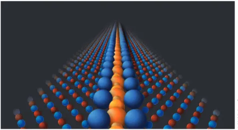
Structural defects play a crucial role in determining the physical and electronic properties of materials, and under-standing the nature of these defects is of key importance in correlating the properties of materials with their structure at the atomic level. A thorough understanding of structural defects requires a precise determination of their three-dimensional structure and chemical composition. In polycrystal-line materials, this goal is complicated by difficulties in investigating defects occurring at the boundary between ad-jacent crystals. Now, Zhongchang Wang and Yuichi Ikuhara from the AIMR and other researchers have developed a method for investigating structural defects using a combination of advanced electron microscopy, spectroscopy and first-principles calculations1.
“Natural materials are often polycrys-talline and their properties are deter-mined by grain boundaries,” explains Ikuhara. Grain boundaries — the inter-face between two crystallite domains or ‘grains’ — trap atomic defects such as im-purities and vacancies which can induce complex structural changes. However, it is difficult to elucidate the distribution and role of self-trapped grain bound-ary defects because of their very low concentration, and the lack of chemical information obtained from conventional electron microscopy methods.
To overcome these difficulties, the researchers devised a methodology that combines different scanning transmission electron microscopy techniques, electron energy-loss spectroscopy and high-precision density functional calculations. Furthermore, special care was taken to design an environment for the electron
microscope that is free from mechanical vibrations and magnetic fields.
Wang, Ikuhara and colleagues applied the methodology on magnesium oxide, a technologically important material that has been studied for decades, but for which the atomic-scale grain boundary structure has remained unknown. To allow the controlled study of individual grain boundaries, the researchers fab-ricated a ‘bicrystal’ consisting of two crystals cut along different crystallo-graphic directions which are joined at their surfaces.
Electron energy loss spectroscopy and transmission electron microscopy mea-surements revealed that titanium and calcium impurities segregate into the grain boundary. More importantly, these impurities interdisperse into the col-umns of magnesium oxide atoms, giving rise to a periodic superstructure along an atomically-straight boundary (see
image). Comparing the experimental re-sults with the rere-sults of the calculations, the researchers were able to pinpoint the structural transformation leading to a stable defect configuration. The analysis further showed that the calcium and titanium are bonded to the oxygen rather than the magnesium atoms.
“This method could in principle be applied to many types of defects in many systems,” says Wang. “The main advantage is that the combination of techniques allows extraction of atomic-scale information on point defects in defective regions, and provides insight into the structure-property interplay at the quantum level.”
1. Wang, Z., Saito, M., McKenna, K. P., Gu, L., Tsukimoto, S., Shluger, A. L. & Ikuhara, Y. Atom-resolved imaging of ordered defect superstructures at individual grain boundaries.
Nature 479, 380 (2011).
Illustration of an ordered defect superstructure forming at a grain boundary in magnesium oxide. The superstructure consists of oxygen (red); magnesium (small blue spheres); and impurities titanium (large blue spheres), and calcium (orange).
Structural defects
Know the boundaries
Understanding the basis of atomic defects and impurities offers greater insight into
the relationship between the structure and properties of materials
© 2012 Ik
uhar
a Gr
Topological insulators are some of the most promising electronic materials available, because they allow the use of the electron’s magnetic property — its spin — for enhanced low-loss computing technology. This advantageous property is based on energy states at the surface, where electrons propagate in a similar way to particles that have no mass. Takashi Takahashi, Seigo Souma and co-workers from the AIMR, with colleagues from Tohoku University’s Physics Department and Osaka University, have now made the surprising discovery that in some topological insulators these elec-trons at the surface state can also show mass, which leads to entirely new effects for spin electronics1.
The difference between normal elec-trons and those in the surface states of topological insulators is that the latter show ‘time-reversal symmetry’, which means, for example, that if the motion of electrons was filmed with a camera, the film would always look the same, whether it is played forwards or back-wards. This time-reversal symmetry is at the core of many attractive properties of topological insulators, including their protection against losses. One feature of this symmetry is that the surface en-ergy states show a characteristic X-shape when electron energy is plotted against momentum (see image).
The researchers have now studied how this X-shape evolves in the topological insulator, thallium–bismuth–selenium. The experiments were performed on an angle-resolved photoemission spec-trometer at the AIMR, which currently has the highest available energy resolu-tion in the world. During the evoluresolu-tion, selenium atoms are increasingly replaced
by sulfur. Because the sulfur analogue, thallium–bismuth–sulfur, is not a to-pological insulator, the replacement of selenium by sulfur enables the tracking of the transition from a topological insu-lator to a classical insuinsu-lator.
With increasing sulfur content, the surface energy states slowly begin to lose their X-shape and a gap opens up in the center of the ‘X’. This means that the electrons no longer appear massless. “There are predictions that topological insulators with a gap show a coupling between magnetic and electronic ef-fects, the strength of which is indepen-dent of the material,” explains Souma. This could be of particular relevance to information storage technologies, because such an effect allows the
control of magnetic information with electrical fields.
The present study makes a compelling case for the technological importance of topological insulators, which continue to be one of the most intensively studied materials today. “Our next step will be to study the origin of this energy gap, which remains poorly understood,” says Souma, adding that an experimental demonstration of the predicted novel effects will also be important.
1. Sato, T., Segawa, K., Kosaka, K., Souma, S., Nakayama, K., Eto, K., Minami, T., Ando, Y. & Takahashi, T. Unexpected mass acquisition of Dirac fermions at the quantum phase transition of a topological insulator. Nature Physics
7, 840 (2011).
From topological insulator to conventional insulator: the evolution from the topological insulator, thallium– bismuth–selenium (top left), to thallium–bismuth–sulfur (bottom right), shows that the ‘X’ shape of the surface states is slowly lost, and a gap in the energy states evolves.
Insulators
Electrons gaining mass
Fr
om Ref
. 1 © 2011 S. S
ouma
The potential of electron surface states of topological insulators has now been considerably
enhanced by the discovery of surface states with a gap in their energy spectrum
The extraordinary physical properties of graphene — a single layer of carbon atoms arranged in a honeycomb lat-tice — and its derivatives such as gra-phene oxide, have excited the interest of scientists and engineers with a view to constructing efficient electronic devices with potentially new functionalities. Graphene-based materials may now also find applications beyond electron-ics. Haixin Chang, Hongkai Wu and co-workers from the AIMR at Tohoku University and institutions in Beijing and Hong Kong believe that graphene’s combination of transparency, flex-ibility and electrical conductivity could enable a wide range of biological and biomedical applications.
At present it remains unclear whether graphene or graphene oxide can be used
in vivo, mostly because their toxicity has
not yet been established. However, these materials could in theory be used as analysis platforms for proteins and cells
in vitro, although the complex interplay
between these materials’ surfaces and cells needs to be better understood before any applications can be realisti-cally considered. In their study of cells attached to multi-layer or ‘few-layer’ graphene oxide films, Chang, Wu and colleagues have demonstrated a way to optimize cell performance by controlling the films’ properties1.
The most direct way of changing the surface properties of graphene oxide is by varying its reduction state. The team achieved this by reducing pristine films to various extents using thermal reduction — a method through which oxygen-containing groups are progres-sively removed when heated. Various aspects of cell behavior were tested
using three different substrates: non-reduced graphene oxide films, and films that had been reduced for 90 and 260 minutes respectively.
The researchers first determined the adsorption of various proteins on the films. They observed that the graphene oxide which had been mod-erately reduced for 90 minutes had the highest adsorption.
This can be explained by considering the combination of conflicting effects arising from the high oxygen content. On the one hand, oxygen promotes hydrogen bonding with the proteins, which increases adsorption. On the other hand, it also induces electrostatic forces and hydrophobic changes, which reduces adsorption.
A similar trend was observed in tests to assess cell adhesion, cell proliferation and cell differentiation. In all cases, the best results were obtained for moderately reduced graphene oxide, which the team ascribes to the stronger protein adsorp-tion obtained in those condiadsorp-tions.
These observations could have serious implications for bio-applications. “The present results open up various possibili-ties to regulate the biological responses in graphene-based materials by control-ling their reduction state,” says Chang.
1. Shi, X., Chang, H., Chen, S., Lai, C., Khademhos-seini, A. & Wu, H. Regulating cellular behavior on few-layer reduced graphene oxide films with well controlled reduction states. Advanced
Functional Materials 22, 751–759 (2011).
Schematic demonstration of the noncovalent interactions between graphene oxide and cellular proteins.
Proteins
Graphene oxide
Graphene oxide
Increased performance through
controlled reduction
© 2011 W
iley
-VCH
Optimized cell performance is achieved through controlling the physicochemical
properties of graphene oxide, leading to intriguing perspectives for bio-applications
The exceptional resilience of bulk metal-lic glasses (BMGs) combined with their high resistance to corrosion and wear makes BMGs a highly sought-after mate-rial in mechanical applications. With a lower thermal conductivity than crystal-line metals, BMGs also offer potential applications in thermal management. Divided into two general groups, BMGs are classified as either metal-metal-based glasses or metal-metalloid-based glasses. Fundamentally, however, the atomic structure of metal-metalloid-based glass-es is still intriguing and remains a matter of debate among experts in the field.
In metal-metal-based glasses compris-ing of only metallic elements, their struc-ture maximizes atomic packing. However, the situation is much more complex for metal-metalloid-based glasses, which also comprise atoms such as phosphorus, boron, silicon and carbon that tend to saturate their charge through covalent and coordination bonds. Because the number, direction, and length of these bonds follow specific rules, they inevita-bly disrupt the dense packing of the metal atoms in metal-metalloid-based glasses.
Until now, it has remained unclear how these contrasting experimental ob-servations can be reconciled. Mingwei Chen, Pengfei Guan and colleagues from the AIMR may have now solved the puzzle by describing a hybrid between a covalent-bond mediated structure and a densely-packed icosahedron structure for a model metal-metalloid BMG, palladium–nickel–phosphorus1.
“This BMG was actually the first bulk metallic glass reported in the literature, and so far it still has the best glass-forming ability among ternary metal-metalloid alloys,” explains Chen.
It was therefore a natural choice for the team to focus on unraveling the structure of palladium–nickel–phos-phorus. In their analysis, the team performed both X-ray diffraction experiments and ab initio molecular dynamics simulations. The results sug-gest that phosphorus coordinates with both palladium and nickel, while metal-lic bonding occurs between these two metallic elements.
The researchers propose the structure of palladium–nickel–phosphorus con-sists of two types of clusters perfectly interconnected, in which tri-capped trigonal prisms centered on phosphorus atoms are linked together by nickel-centered densely-packed icosahedra.
This hybrid structure, which satisfies both the necessity of charge saturation
for phosphorus atoms and the dense packing requirement for metal atoms, exhibits the lowest energy achievable in the compounds and is therefore relatively disordered, yet stable.
These findings do not only explain the well-known glass-forming ability of the alloy palladium–nickel–phosphorus, but also hold a wider significance in our understanding of the formation of metal–metalloid glasses. “This may be a universal structural model for metal– metalloid glasses,” says Chen. “We have also found the same packing scheme in different alloy systems.”
1. Guan, P. F., Fujita, T., Hirata, A., Liu, Y. H. & Chen, M. W. Structural origins of the excellent glass-forming ability of Pd40Ni40P20.
Physical Review Letters 108, 175501 (2012).
Atomic structure of the bulk metallic glass, palladium–nickel–phosphorus, comprised of phosphorus (pink); nickel (green); ordered palladium (blue) and disordered palladium (red).
Bulk metallic glasses
An unexpected hybrid
© 2012 APS
A combined experimental and theoretical study reveals a hybrid structure for
metal-metalloid bulk metallic glasses that reconciles previously contradicting observations
The surfaces of polymers — large molecules comprising repeated struc-tural units — contain special physical properties such as adhesion, wetting, and friction. These properties can be quite different from those of the bulk material, and are difficult to correlate with the polymers’ molecular structures. Although modern synthetic strategies offer much control over molecular struc-ture, finding the optimum polymer for a particular device or application remains a challenge. Ken Nakajima, Dong Wang and co-workers1 from the AIMR at
Tohoku University have now succeeded in mapping out the surface properties of a polymer film using atomic force microscopy (AFM).
Nakajima describes the concept of mapping properties with a simple illus-tration: “Consider painting a colored ink on a polymer surface — the color will be more easily erased from areas with lower adhesive properties.” Polymer properties such as viscoelasticity and adhesion hold great potential in a variety of applica-tions, including automotive manufactur-ing. “It is clear that this work may be directly applicable in the production of polymer materials for tires, for which adhesive and viscoelastic properties are important. Indeed, we are currently col-laborating with several tire companies in Japan,” says Nakajima.
In the past, measurements of tensile or shear stress have been used to evalu-ate adhesive strength and viscoelastic behavior. These methods, however, are a macroscale examination and provide only an average value of properties. In contrast, AFM uses an atomically thin tip attached to a flexible lever to directly probe the properties of the surface at
the nanoscale. Here the research team used contact-mode AFM, described by Nakajima as “a nanomassage” in which the polymer’s molecular structure consists of a block of poly(ethylene-co-butylene) sandwiched between two blocks of poly(styrene) — a tri-block copolymer. Rather than being homog-enously mixed, the polymer molecules in the bulk are arranged so that ‘blocks’ of similar polymer are close together. At the surface, this is manifested as a pattern of many small polymer ‘islands’ (see image). “Our AFM technique al-lows us to prepare a map of how the surface properties vary over the surface,” explains Nakajima.
This technique holds promise in the mapping of mechanical surface
properties for other types of block co-polymer, provided there is a mechani-cal difference between the different components. “In the future we hope to characterize the surface properties of other materials such as bulk metallic glasses and biomaterials,” says Nakajima. “Ultimately we are hoping to establish a connection between the macroscopic properties of the polymer and a nano-scopic understanding of structure which we can then use to evaluate and design new high performance materials.”
1. Wang, D., Liang, X-B., Liu, Y-H., Fujinami, S., Nishi, T. & Nakajima, K. Characterization of surface viscoelasticity and energy dissipation in a polymer film by atomic force microscopy.
Macromolecules 44, 8693–8697 (2011).
A map of viscoelastic properties of a tri-block copolymer sample.
AIM RESEARCH
1 μm
Polymer properties
Macromolecular mapmaking
Probing the surface properties of polymers could help to bridge the gap between
their macroscale properties and their nanoscale structure
© 2011 A
Topological insulators exhibit some of the most fascinating conductive prop-erties of any material. Although the bulk volume of a topological insulator does not pass any current, its surface is highly conductive and the magnetic spin orientations of the surface cur-rents are relatively easy to preserve. This unique behavior has stimulated studies into both the fundamental sci-ence behind these properties and ap-plications such as ultralow-power spin transistors. Toshiyuki Arakane, Takashi Takahashi and colleagues at Tohoku University and Osaka University have now developed a topological insulator material that should aid research in this area1.
The researchers focused on an out-standing problem in the field: the bulk of a topological insulator often has defects through which current can flow. This bulk current can obscure surface currents whose behavior is the intend-ed subject of the experiment. Previous work by other researchers showed that manipulating the elemental composi-tion of a topological insulator can reduce its bulk conductivity while maintaining high surface conductivity.
Arakane and co-workers took this work a step further by showing that manipulating the composition of a topological insulator can keep its bulk conductivity low while also allowing the surface current to be tuned between positive and negative charge carriers. They chose to investigate BSTS — a ma-terial made from bismuth, antimony, tellurium and selenium (see image). BSTS is known to have two types of crystal defects: one that contributes positive charge carriers, and one that
contributes negative charge carri-ers. Careful control over the relative amount of each element allowed the researchers to balance these defects, thus minimizing the bulk conductivity.
Through angle-resolved photoemis-sion spectroscopy, the researchers re-vealed that this compositional control can also be used to adjust the energy of the surface charge carriers. They were able to tune the surface carriers to the Dirac energy point, where their concen-tration fell to zero. Furthermore, they successfully tuned the carrier energy to either below or above the Dirac energy point, thus causing the surface carriers to take on positive or negative charac-ter, respectively. In both situations, the bulk conductivity remained low.
According to Arakane, this research should allow a variety of exotic quan-tum effects to be observed. “We expect to see effects such as the topological magneto-electric effect, the quantum spin Hall effect and excitonic con-densation — all of which have been proposed theoretically but not yet ob-served experimentally due to the bulk carrier problem.” Device applications, says Arakane, would benefit from thin-film growth techniques, which will be a future focus of the research group.
1. Arakane, T., Sato, T., Souma, S., Kosaka, K., Nakayama, K., Komatsu, M., Takahashi, T., Ren, Z., Segawa, K. & Ando, Y. Tunable Dirac cone in the topological insulator Bi2–xSbxTe3–ySey.
Nature Communications 3, 636 (2012).
Tunable Dirac cone in topological insulator Bi2-xSbxTe3-ySey. Controlling the composition ratio of Bi/Sb and Te/
Se leads to the change in the filling of Dirac carriers while keeping the bulk insulating nature.
Topological insulators
Conduction gets a tune-up
© 2012 T
oshiyuk
i A
rak
ane
Tuning the composition of a topological insulator material has allowed scientists
to control its intriguing surface properties while preventing current from leaking
through the bulk
With their unique properties of excep-tional mechanical strength, high elastic-ity, and resistance to mechanical wear, bulk metallic glasses hold great potential in the design of micromechanical devices and nanoscale catalysts. Although the production of nanoscale metallic glass structures is already underway, the tech-niques used are too expensive and time-consuming to lend themselves to mass production. Koji Nakayama, Na Chen and colleagues from the AIMR and the Institute for Materials Research at Tohoku University have now discovered a new, cost-effective technique to pro-duce metallic glass nanowires that yields at least a few hundred million nanowires per gram of material1.
Unlike the structure of crystalline met-als, metallic glasses have an amorphous and tightly-packed atomic structure, which makes them tough and resistant to mechanical deterioration. Metallic glasses are produced using a melting pro-cess, in which the molten liquid requires a high viscosity, as well as a high “spin-nability” — a tendency to form elongated shapes — in order to yield nanowires.
Nakayama and his team found they could create these conditions in a process called gas atomization, commonly used in the production of metallic powders. During this process, molten metal flows from the nozzle of a crucible and meets high-speed gas at the exit, which breaks up the metal stream into a variety of particulate shapes (see image). By supercooling the molten alloy below its melting point, the researchers could increase the viscosity of the melt stream prior to the gas atomization process. Though unremarkable to the naked eye, the atomized products form a metallic
lump that contains a tangle of long me-tallic glass nanowires with diameters of 50–2,000 nanometers.
“The length to diameter of the wire (aspect ratio) increases exponentially with decreasing temperature below the melting point,” explains Nakayama, who established a “spinnability rule” to predict how nanowires made from different me-tallic glasses have an aspect ratio that is dependent on atomization temperature.
The team has so far focused on two metallic glasses — Zr65Cu18Ni7Al10 and Fe76Si9.6B8.4P6 — but plans to make nanowires that contain important catalytic elements like platinum and palladium. “Metallic glass nanowires
will have a significant impact on catalyst research,” says Nakayama. Since nanow-ires have a large surface-area-to-volume ratio, they are more catalytically active per gram of material — one of the goals of green chemistry. In future, such metal-lic glass nanowires may also be formed from magnetic elements, which could have useful applications in the design of miniature devices with a high-frequency impedance response to a changing magnetic field.
1. Nakayama, K. S., Yokoyama, Y., Wada, T., Chen, N. & Inoue, A. Formation of metallic glass nanowires by gas atomization. Nano Letters
12, 2404–2407 (2012).
Gas atomization, a process for making metallic particles, can be used to fabricate metallic glass nanowires. Molten metal flows from a crucible nozzle and interacts with a high-speed gas to break down the metal stream into various particulate shapes, including nanowires (inset).
nanowire
Bulk metallic glasses
Nanowire gems in the particle dust
© 2012 A
CS
A cost-effective method for creating metallic powders helps to accelerate the
production of metallic glass nanowires
An important characteristic critical to a variety of technologies is the way in which oxide materials trap charges. For example, hafnium dioxide — used to insulate transistor gate electrodes — can begin to fail if charges become trapped in its bulk. Similarly, the effectiveness of zirconium dioxide as a common catalyst depends on the quantity of trapped charges. Accurately predicting the nature of charge trapping in oxides like these, however, has remained an unmet challenge. Now, Keith McKenna and Alexander Shluger from the AIMR at Tohoku University, along with col-leagues from the UK and the USA, have developed a new calculational approach to predict unexpected aspects of charge localization — and thus trapping — in oxides1.
Calculations of charge trapping gen-erally rely on density functional theory (DFT). The widely used implementa-tions of DFT, however, characterize electrons as interacting with themselves electrostatically — a physically incorrect description. This ‘self-interaction error’ leads to inaccurate predictions of charge trapping in materials. McKenna, Shluger and colleagues have now carried out calculations using a version of density functional theory that includes cancella-tion of nonlinearity — that is, a correc-tion to the self-interaccorrec-tion problem. This new insight provides an unprecedented view into how charges are localized in hafnium oxide and zirconium oxide.
Although usually considered to be three-dimensional bulk crystals, the researchers’ calculations predicted that charges in these materials behave as if they were constrained to two dimensions. This is because the crystal
structure of each material consists of al-ternating layers, in which oxygen atoms coordinate — or bond — to either three or four metal atoms. When a positive charge is induced in the materials, it induces distortions in the surrounding crystal lattice, and in turn quickly sta-bilizes the lattice structure (see image). The positive charge together with the lattice distortions are referred to as a polaron.
The researchers found that polarons prefer to stay in oxide layers with triply coordinated oxygen atoms. Such two-dimensional behavior has been much studied due to the particular physics it involves, but it has typically been ob-served only in complex oxides composed
of three or more types of atoms, or at interfaces between materials. Its obser-vation in a relatively simple binary oxide, made of only two types of atoms, is un-expected and will lead to a new investi-gative approach of the particular physics involved. “In addition to the importance of the theoretical methods themselves, our predictions may stimulate new studies of the correlated dynamics and interaction of positive charges in binary oxides,” says McKenna.
1. McKenna, K. P., Wolf, M. J., Shluger, A. L., Lany, S. & Zunger, A. Two-dimensional polaronic behavior in the binary oxides m-HfO2 and m-ZrO2. Physical Review Letters
108, 116403-1–116403-5 (2012).
A positive charge (blue) inside the crystal lattice of hafnium oxide is initially dispersed in three dimensions (left). The charge brings about slight distortions in the crystal lattice which causes it to localize to a two-dimensional sheet (right).
Oxide materials
Hidden layers
© 2012 APS
A new calculational approach predicts that charges trapped in simple and common
three-dimensional bulk oxides are restricted to two-dimensional sheets
Electroactive and short-lived species that are released and consumed by cells, including neurotransmitters and reactive oxygen-based molecules, are central to cell metabolism, but their detection at cell surfaces and interfaces remains challenging. A research team led by Tomokazu Matsue and Yasufumi Takahashi from the AIMR1, in
collabora-tion with Yuri Korchev from Imperial College London, has now developed a high-resolution, non-invasive imaging method called voltage-switching mode– scanning electrochemical microscopy (VSM–SECM). The technique, which can be utilized under physiological condi-tions, provides high-quality topographi-cal and electrochemitopographi-cal images of living cells simultaneously.
Many SECM imaging approaches have been developed to determine surface topology and reactivity. However, they usually measure interactive forces by direct contact, through the tip of a tiny electrode that moves across the surface of the substrate being imaged — which can damage cell membranes.
Matsue and colleagues have now used faradaic current, which is generated by the reacting electroactive species, to control the motion of the electrode, and continuously prevent it from touching the substrate surface. Moreover, they fab-ricated nanometer-sized glass-insulated carbon electrodes that allow for high-resolution imaging.
To initiate one measurement, the team moved the electrode tip towards the sur-face while monitoring the distance-de-pendent current created by the hindered diffusion of the electroactive species as they underwent reduction. When the tip current decreased to a level that reflected
the desired distance between probe and either the substrate surface or an electro-active molecule, the researchers stopped the probe and recorded its position. At each position, the team switched the voltage applied to the electrode to also determine the species’ activity. Repeating this process at several points across the surface yielded simultaneous topograph-ical and electrochemtopograph-ical images.
Similar to ultra-high resolution im-ages, the resulting maps highlighted the small protrusions and wave structures of skin and cardiac cells as well as elongated hair cells (see image). Visualization of cell membrane proteins associated with cancer showed that the protein distribu-tion was uneven and did not match the ultra small features observed from the topological images — demonstrat-ing the usefulness of VSM-SECM for chemical mapping at biological interfaces. Simultaneous topological
and electrochemical measurements have also enabled Matsue’s team to detect the release of neurotransmitters from neurons. Furthermore, the combination of SECM with fluorescence microscopy clearly showed the extremities of neurons at the synapse.
Currently, the researchers are further exploring neuronal communication using their new method. “We would like to map the neurotransmitter releas-ing sites,” says Matsue. The team is also planning to monitor the release-related changes in neuron topography.
1. Takahashi, Y., Shevchuk, A. I., Novak, P., Babaki-nejad, B., Macpherson, J., Unwin, P. R., Shiku, H., Gorelik, J., Klenerman, D., Korchev, Y. E. & Matsue, T. Topographical and electrochemical nanoscale imaging of living cells using voltage-switching mode scanning electrochemical microscopy.
Proceedings of the National Academy of Sciences USA 109, 11540–11545 (2012).
Topographical image of hair cells acquired by the VSM–SECM imaging technique.
Cell imaging
Switching it up
© 2012 PNA
S
A state-of-the-art technique that enables simultaneous topographical and
electrochemical imaging of interfaces creates new opportunities for the chemical
mapping of living cells
Spintronics is an emerging technol-ogy which exploits the intrinsic angular momentum — or, spin — of electrons for new efficient ways of storing and processing information. In contrast, in conventional electronics only the charge of the electron has a central role. A basic requirement for spintronics devices is the availability of electrons in well-defined, rather than random, spin states. Akari Takayama and colleagues from the AIMR at Tohoku University, together with collaborators from Osaka University, have now found an approach to producing such ‘spin-polarized’ electrons, with the important feature that the degree of spin polarization can be tuned1.
Traditionally, the production of spin-polarized electrons involved ferro-magnetic materials, in which spins are naturally aligned. For device applica-tions, however, electric fields are often preferred to magnetic ones. A general approach to the electric generation of spin polarization is through ‘spin–orbit coupling’, which connects the charge of an electron with its spin. One mani-festation of spin–orbit coupling is the Rashba effect, in which electrons are polarized when certain types of asym-metries — typically found at the surface of materials — are present.
Takayama and colleagues have stud-ied the Rashba effect in very thin films of the metal bismuth. They deposited films of thickness ranging from 16 to 80 atoms on a silicon surface. To their surprise, they observed in these samples that the spin-polarizing effect was at work not only on the surface, but also at the interface between the metal film and the silicon substrate (see image).
“This result was unexpected, as the simple Rashba picture suggests the exis-tence of spin-polarized electrons only at the top surface of our samples,” explains Takayama. Furthermore, the effects on the two sides of the film were found to interfere with each other. As a result of this interaction, the degree of polariza-tion decreased when the sample was made thinner. “This is the most surpris-ing result of our study: spin polarization can actually be tuned by varying the thickness of the film,” says Takayama.
The researchers’ choice of bismuth for their study was no coincidence. Spin– orbit coupling is particularly strong in
materials made from bismuth or other heavy elements, such as gold or antimo-ny. Now that Takayama and colleagues have shown that the degree of polariza-tion is tunable through the thickness of the films used, materials such as bismuth hold even greater promise for future applications in next-generation spintronics devices, for enhancing spin-polarized currents, and for fundamental studies of novel quantum effects.
1. Takayama, A., Sato, T., Souma, S., Oguchi, T. & Takahashi, T. Tunable spin polarization in bismuth ultrathin film on Si(111). Nano Letters
12, 1776–1779 (2012).
The effect of spin-polarization is seen as expected at the surface of a thin bismuth film (upper plane) but also, surprisingly, at the interface with the underlying silicon substrate (lower plane).
AIM RESEARCH
Spintronics
Both sides polarized
© 2012 Ak
ari T
ak
ay
ama
The finding that a spin effect — important in spintronics — can be present at both sides
of a thin metal film suggests a route to a tunable source of spin-polarized electrons
Traditional methods of culturing cells for biological and biomedical applica-tions use two-dimensional cell cultures, typically growing cells on the base of plastic Petri dishes. In recent years, however, a three-dimensional (3D) en-vironment has emerged as more appro-priate for cell culture as it replicates the biological milieu. This is particularly important for embryonic stem cells which can grow into a variety of dif-ferent tissue structures (such as bone, nerve, cartilage cells) from 3D embryoid bodies. Researchers from the AIMR and the Graduate School of Environmental Studies at Tohoku University have now built an electrochemical device that monitors the activity and differentiation of stem cells in an embryoid body1.
Usually, scientists label biomolecules for analysis with fluorescent markers to identify and quantify their presence. But labelling molecules may be toxic or interfere with cellular behavior, and fluorescence levels can be compromised by autofluorescence (signals from unlabeled molecules) or quenching from other non-target materials or liquid turbidity. The electrochemical device developed by Tomokazu Matsue, Kosuke Ino and colleagues does not require these labels, thus removing these problems.
Electrochemical detection has been used before. However, this device has a unique feature. Detection is achieved using an array of 256 electrochemical sensors with only 32 bonding pads for external connection (see image), placed at the base of deep microwells which enables spatially-resolved measure-ments. “This electrochemical sensor density is the highest in the field of
electrochemical lab-on-a-chip devices,” the researchers explain.
The research team quantified cellular activity from embryoid bodies on the array by ‘redox cycling,’ whereby alka-line phosphatase activity (a marker for the differentiation level of embryonic stem cells) was measured by the reduc-tion and oxidareduc-tion of one of its reacreduc-tion products. Potentials of electrodes in each sensor were set at levels to initiate redox cycling at a specific location from which the local current signals were collected and measured.
Interestingly, enzymatic activity as measured by the electrode device after a four-day incubation did not increase as expected, suggesting that the stem cells had differentiated. The device will therefore be useful to screen embryoid bodies’ differentiation levels, and will
provide more quantitative than conven-tional sorting by morphological analysis.
Furthermore an embryoid body resting on top of the sensor array was imaged without cross-talk from mo-lecular diffusion between sensors due to the microwells. In the next stage of this project, the researchers will explore the limits of this imaging capability.
“We intend to increase the density of the electrochemical sensors even fur-ther for electrochemical imaging of a single cell or a single tissue,” say the researchers.
1. Ino, K., Nishijo, T., Arai, T., Kanno, Y., Takahashi, Y., Shiku, H. & Matsue, T. Local redox-cycling-based electrochemical chip device with deep microwells for evaluation of embryoid bodies.
Angewandte Chemie International Edition
51, 6648–6652 (2012).
Optical image (left) of the embryoid bodies sitting on top of individual sensors. The electrochemical image (right) shows the embryoid bodies detected using the lab-on-a-chip device.
500 μm 500 μm
Lab-on-a-chip
Electrochemical imaging
© 2012 W iley -VCH V erlag GmbH & C o. K G aA, W einheimA high-density electrochemical device has been developed to monitor and image
stem cells in three-dimensional embryoid bodies
Bone health hinges on the assembly of various cells, including osteoblasts and osteoclasts, into well-defined functional structures that manage bone-specific tasks in the body, such as cell growth, differentiation and protein secretion. However, tumor-induced injuries and other bone-related diseases hinder these self-regulated, sophisticated tasks. To address these conditions it is essential to develop tissue engineering approaches that direct cell behavior.
Xuetao Shi and Hongkai Wu and co-workers from the AIMR at Tohoku University, together with colleagues in Hong Kong and Beijing1, have now
developed patterns that serve as scaf-folds for bone regeneration. The patterns consist of polymer microspheres filled with drug or protein molecules that are regularly interspaced.
Prevalent methods for directing cell behavior exploit either chemical and bio-logical signals or topographical cues, but using each of these methods separately has proven ineffective. The former approach can regulate stem cell differentiation into specialized cells but does not properly control cell spatial arrangements, while the latter faces opposite limitations.
By combining both approaches into microsphere patterns, the researchers have now taken advantage of chemical and physical stimulations at the same time. The patterns induced an aligned growth of cells that simulates the native surfaces of bones and the membrane enveloping their outer surface. “We also used the microspheres to encapsulate and release drug molecules to mimic the in
vivo bone environment, which contains
various beneficial substances such as growth hormones,” adds Shi.
To create the patterns (see image), Shi’s team first mixed an organic solu-tion containing the biocompatible, biodegradable poly(lactic-co-glycolic acid) polymer with a drug or protein dis-solved in water in the presence of emul-sifiers. After depositing the resulting microspheres onto a patterned Teflon mold and adding a solvent to ensure inter-particle cohesion, the researchers covered the mold with a Teflon slide and applied pressure to this lid to obtain the patterned material.
Initial tests showed that patterns with narrow grooves between the microspheres resulted in better cell alignment than wide ones. Moreover, the microspheres efficiently encapsu-lated and slowly released hydrophilic and hydrophobic molecules, prompt-ing the researchers to simultaneously load multiple drugs into them. Stem
cells cultured on these multi-drug-loaded patterns exhibited high levels of bone tissue formation markers, proof of their enhanced differentiation towards osteoblasts.
In addition to bone repair, this com-bined chemical–topographical strategy can be used to study muscle and blood vessel cells for potential regenerative therapies of cardiac tissues. “Our future work will focus on further developing scaffolds displaying surfaces that mimic native tissue and drug or gene release function for organ and tissue regenera-tion,” says Shi.
1. Shi, X., Chen, S., Zhou, J., Yu, H., Li, L. & Wu, H. Directing osteogenesis of stem cells with drug-laden, polymer-microsphere-based micropatterns generated by Teflon microfluidic chips. Advanced Functional Materials
22, 3799–3807 (2012).
Schematic representation of the microsphere pattern manufacturing process.
Teflon stamp
Drug-laden polymer microsphere
Pressure Microsphere-based micropattern
Biomaterials
Stimulating patterns
© 2012 X . ShiMicroscopic patterns made of tiny drug-filled polymer spheres stimulate stem cell
growth and differentiation for bone tissue repair
Twenty-five years ago, nobody thought that gold would have catalytic activity towards molecular oxygen, because clas-sical thermodynamic principles reject any chemical reaction between gold and oxygen. But the discovery that gold particles smaller than five nanometers could oxidize carbon monoxide (CO) into carbon dioxide (CO2) at room tem-perature set off flurries of investigation. Soon, researchers had harnessed this size-dependent catalysis for applications such as decontaminating hydrogen gas in polymer fuel cells. The underlying mechanism for this catalytic activity however remains unclear.
Mingwei Chen, Takeshi Fujita, and co-workers from the AIMR at Tohoku University, in collaboration with re-searchers from Japan, the US, the UK and China, have captured new evidence that small defects on gold surfaces are active sites for CO oxidation reactions1.
By developing state-of-the-art tech-niques to watch surface atomic struc-tures evolve as catalysis occurs, the team also discovered that impurity atoms play critical roles in stabilizing the defect sites — a finding that could boost the longevity and activity of gold catalysts.
Most nanoparticles require an oxide support to hold them in place, making it difficult to pinpoint specific gold cata-lytic mechanisms. Chen and his team overcame this problem by studying a substance known as nanoporous gold.
Produced by electrochemical de-alloying of a thin gold–silver precur-sor film, it has a three-dimensional, free-standing architecture of curved nanopores, making it ideal to study gold catalysis without interference from other materials.
The researchers turned to spherical-aberration-corrected scanning transmis-sion electron microscopy (Cs-corrected STEM) to identify catalytically active nanoporous gold surface structures. This technique suppresses lattice dis-tortion effects caused by projection lenses, providing sub-atomic resolution capabilities. By carefully controlling gas pressures within a specially-designed specimen holder, the team performed
in situ characterizations during a CO
oxidation reaction in an environmental TEM. “Cs-corrected STEM gives us a great chance to see the true atomic struc-ture of complex materials,” says Chen.
The team’s high-resolution images revealed that nanoporous gold’s surface structure consists of flat, close-packed terraces separated by single-atom steps (see image). Along bent por-tions of the nanopores, these steps fall out of alignment and become ‘kinks’
of under-coordinated gold atoms — exceedingly active sites for chemical oxidation. When the researchers ex-posed the nanoporous gold to a CO/ air gas mixture, they observed that the terrace edges dynamically recon-structed into kinked arrangements, a clear sign that these defects play critical catalytic roles. Further experiments revealed that residual silver impurities in nanoporous gold preserved the high density of kinked defects, ensuring high catalytic performance.
Chen notes: “Although many theories have been put forward before, the story of gold catalysis is simpler than anyone ever thought.”
1. Fujita, T., Guan, P., McKenna, K., Lang, X., Hirata, A., Zhang, L., Tokunaga, T., Arai, S., Yamamoto, Y., Tanaka, N. et al. Atomic origins of the high catalytic activity of nanoporous gold.
Nature Materials 11, 775–780 (2012).
A scanning transmission electron microscopy image showing the stepped surface of nanoporous gold.
2 nm
Catalysis
A kink in the golden rules
© 2012 Natur
e P
ublishing Gr
oup
High-resolution imaging of nanoporous gold reveals that ‘kinked’ surface defects are
responsible for its high catalytic activity in carbon monoxide oxidation
Synthetic dyes with long-lasting, vivid colors are valuable to both manufacturers and consumers. However, these attributes also make it challenging to clean up these compounds when they slip into wastewa-ter systems and become pollutants. ‘Azo’ dyes, for example, owe their colors to nitrogen double bonds that resist degra-dation from bacterial or carbon sorption treatments. Now, Jun-Qiang Wang from the AIMR at Tohoku University1 and
co-workers in Japan and the US have described a way to degrade azo dyes with far greater efficiency than current techniques, using amorphous magne-sium–zinc metallic glass powders.
One of the best ways to decompose azo dyes is by using pure, ‘zerovalent’ metals — in an oxidation state of 0 — such as magnesium or iron to transfer electrons to nitrogen double bonds and crack them apart. However, although zerovalent magnesium is particularly effective at removing organic contami-nants from water, it has poor corrosion resistance and is eventually consumed by the aqueous environment. Materials researchers are thus focusing on finding low-cost methods to reduce the corro-sion of magnesium while retaining its high reaction efficiency.
Alloying magnesium with another metal can enhance its resistance to cor-rosion, but only if the atoms are mixed together well. To achieve this, Wang and his co-workers melted magnesium and zinc atoms in a crucible, and then quick-ly cast them into thin ribbons of metal-lic glass. The metal atoms pack tightly and homogenously in this glassy state, giving the alloy excellent durability.
Then, to convert the magnesium-zinc ribbons into a form suitable for treating
wastewater, the team pulverized them into a fine powder — an unconventional approach that has many advantages, ac-cording to Wang.
“Powders have much larger surface areas compared to ribbons, which en-hances their reactivity,” he says. “Also, the powdered form may be injected underground to deal with pollutants in groundwater.”
Microscopy experiments revealed that the magnesium–zinc powder was well dispersed and did not form ag-gregates (see image), making it ideal for reacting with synthetic contaminants in an aqueous solution. The powder de-colored a solution of azo dye within 10 minutes — clear evidence that the metallic glass completely degraded stubborn nitrogen double bonds.
Wang notes that in addition to a striking improvement in corrosion resistance, which the researchers at-tribute to the alloy’s amorphous atomic structure, magnesium–zinc metallic glass powders can decontaminate azo dyes with reaction efficiencies 1,000 times greater than that of commercial iron powders.
“These materials can efficiently degrade organic water contaminants in harsh, anaerobic environments at a cheap price, opening up a broad field for metallic glass applications.”
1. Wang, J.-Q., Liu, Y.-H., Chen, M.-W., Louzguine-Luzgin, D. V., Inoue, A. & Perepezko, J. H. Excellent capability in degrading azo dyes by MgZn-based metallic glass powders.
Scientific Reports 2, 418 (2012).
A high resolution scanning electron microscopy image of a metallic glass powder that efficiently decontaminates dye molecules from wastewater.
Bulk metallic glasses
Taking the color out of
polluting dyes
© 2012
J.-Q
. W
ang
Dye molecules that contaminate effluent streams can be efficiently degraded by
metallic glass powders
Natural tissues are highly organized structures, often formed from mul-tiple cell types precisely positioned to carry out their required roles. Efforts to mimic these structures in order to create artificial tissues — for example, to help heal parts of the body that have sustained damage from injury or dis-ease — is no simple task.
Recently developed techniques such as dielectrophoresis use electric fields to position living cells within a three-dimensional matrix; however, trapping the cells in place while en-suring their long-term viability has proven difficult. A highly biocompat-ible scaffold material that could solve this problem has now been identified by an international team of research-ers led by Ali Khademhosseini and Tomokazu Matsue from the AIMR at Tohoku University1.
The researchers selected a semi-natural hydrogel material based on gelatin — gelatin methacrylate (GelMA) — to use as a tissue scaffold. Previous studies have shown that GelMA is a suitable material for culturing cells. The researchers also observed that GelMA had the capability to bypass the typical pitfalls of the most commonly used tissue engineering scaf-folds. “Owing to its low viscosity and con-ductivity, we suspected that the GelMA hydrogel could be a promising candidate for cell manipulation using the dielectro-phoresis method,” says Samad Ahadian, a member of the AIMR team.
Testing GelMA in the laboratory, the researchers confirmed that it was a suitable matrix within which to guide cells into position using dielectropho-resis. Once the cells were in place, the team exposed the scaffold to UV light.
This triggered a chemical cross-linking reaction within the hydrogel, which forms the polymer matrix and traps the cells in place. Using a photomask, the researchers were able to trap one type of cell in one part of the polymer before introducing and trapping a second cell type within the same scaffold.
Crucially, the cells retain long-term viability after the formation of the cross-linked polymer, and read-ily proliferate over several days (see image). The natural gelatin on which the hydrogel is based is responsible for this high biocompatibility. “The GelMA comprises natural cell-binding motifs that support cell adhesion, migration, and proliferation,” explains Ahadian. “The optimized GelMA concentration
of 5% ensures that there is plenty of space for the encapsulated cells to obtain the nutrients required and repel wasted products.”
The next step will be to produce engineered tissues with differentiated cell types, from neural to muscle cells. According to Ahadian, the potential applications extend beyond damaged tissue repair to include uses in drug screening models or as bio-actuators.
1. Ramón-Azcón, J., Ahadian, S., Obregón, R., Camci-Unal, G., Ostrovidov, S., Hosseini, V., Kaji, H., Ino, K., Shiku H., Khademhosseini, A. & Matsue, T. Gelatin methacrylate as a promising hydrogel for 3D microscale organization and proliferation of dielectrophoretically patterned cells. Lab on a Chip 12, 2959–2969 (2012). By using a GelMA scaffold, precisely positioned cells are able to grow over several days of culture.
Day 1
Day 3
Day 5
Tissue engineering
A scaffold for longer-lasting cells
© 2012 Ro
yal S
ociet
y of Chemistr
y