Thermal Oxides Formed on Silicon Substrates
2004
Shigeto Fukatsu
Abstract
Thermal silicon oxide (SiO2) is the most important gate insulating material in the silicon (Si) MOSFET technology today. The thermal Si oxide also plays an important role in the development of next generation gate insulator materials (e.g., high dielectric constant materials) because it continues to exist as an interfacial layer between the new gate material and Si wafer. The improvement of MOSFET performance has been achieved in the past by miniaturization. However, with the gate length reaching 100nm and below, it is becoming increasingly difficult to realize thinner gate insulators and smaller channel lengths while maintaining the normal state of device operation. Lack of a precise atomic level picture of thermal oxidation mechanisms is interfering with development of future nanoscale thermal oxides. A phenomenon such as diffusion of boron (B) from the top polycrystalline silicon gate electrode to the Si channel region through SiO2 gate insulator is smearing the well-defined channel in Si.
In order to overcome these problems, experimental investigations of Si and B diffusions in thermal SiO2 formed on Si wafers followed by complete numerical modeling of the data were performed in the present study. The precise knowledge of Si self-diffusion in SiO2 is indispensable for the development of future gate insulator architecture. Understanding of the B diffusion in SiO2 is important to prevent the smearing of the channel region. In this study, 30Si stable isotopes and B impurities embedded in isotopically enriched28SiO2 were employed as diffusion markers, and the diffusion of Si and B in SiO2 as a function of the diffusion annealing temperature, annealing time, and thermal oxide thickness were investigated with and without surface silicon nitride (Si3N4) layers placed on the SiO2 films. The depth profiles of 30Si and B before and after annealing were determined by secondary ion mass spectrometry (SIMS). As a result, Si diffusivity obtained without surface nitride does not depend on the thickness of the SiO2 film and agrees with the previously reported value of Si diffusivity in the bulk quartz. Such Si diffusivity remains the same for a variety of oxygen partial pressures in the annealing atmosphere, when there is no nitride layer on the top. On the other hand, when the nitride layer is placed, the Si diffusivity was found to increase as the thickness of the SiO2 film is reduced. In order to understand this phenomenon quantitatively, we proposed a new picture in which SiO molecules generated at the SiO2/Si interface due to SiO2+Si→2SiO reaction diffuse into the SiO2 layer and enhance the Si diffusivity. Numerical simulations conducted based
on this model for our variety of experimental conditions yield very good quantitative agreement with the experimental results, supporting the hypothesis used to developed the model. Similar experimental results were obtained for boron diffusion in SiO2 depending on the presence of the surface nitride layer, and the model assuming SiO enhancing the diffusion of B in SiO2 reproduce our experimental results quantitatively.
In summary, we have performed experiments probing Si and B diffusion in SiO2formed thermally on Si wafers, and discovered that SiO molecules generated at the SiO2/Si inter- face enhanced the Si and B diffusion when the nitride cap was placed. A unified math- ematical model describing the correlated diffusion of Si and B developed in this study should be incorporated in the next generation Si process simulation software in order to increase the precision of the simulated outcome. It will be also of great interest in the future to develop new nanoscale Si fabrication technique utilizing the role of SiO defects.
Acknowledgement
First of all, I would like to express my sincere gratitude to my research advisor Prof.
K. M. Itoh for his sincere guidance, helpful suggestions, and substantial supports, which were certainly the most essential help throughout this work.
I am grateful to Dr. M. Uematsu of NTT Basic Research Laboratories for kind supports and guidance. I have benefited from his keen physical insight and open manner of sharing knowledge.
I would like to extend many appreciations to Prof. E. Ohta, Prof. Y. Fujitani, and Prof. H. Imai for their careful review of this manuscript.
I would like to thank Prof. K. Shiraishi, Dr. H. Kageshima, Dr. A. Fujiwara, Dr. K.
Nishiguchi, Prof. Y. Takahashi, and Dr. H. Inokawa for their helpful supports, suggestions, and discussions. They supported my work at NTT basic research laboratories in many ways.
I also learned a lot in discussions with Prof. U. G¨osele, Prof. K. Yamada, and Prof.
E. E. Haller.
I would like to extend appreciations to Prof. Y. Shiraki and Prof. K. Nakagawa. They accepted me to perform experiments in Prof. Shiraki’s group of the University of Tokyo.
I acknowledge Dr. T. Ueno, Dr. M. Miura, Dr. K. Kawaguchi, Dr. T. Irisawa, Dr. K.
Odaira, H. Miura, K. Sawano, S. Tokumitsu, and S. Otake, of Shiraki’s group, for their kind support and encouragement.
I thank A. Takano for SIMS measurement.
I acknowledge A. Fujimoto and T. Mitani for TEM measurements, SIMS measure- ments, and their kind support.
I acknowledge kind supports by members in Prof. Itoh’s research group: Dr. T.
Sekiguchi, Dr. K. Morita, Dr. J. Kato, T. Arai, K. Takyu, T. Morita, Y. K. Kato, T.
Itoh, A. Kurokawa, Z. Miyazaki, T. Ishikawa, E. Abe, T. Takahashi, T. Kojima, K. Kojima, T. Yamada, R. Nebashi, T. Ohya, Y. Matsuki, Y. Shimizu, S. Yoshida, D. Tsurumi, M.
Tsuchiya, and many others. The present work would not have been possible without their generous help.
Finally I would like to extend my deepest appreciation to my family for their warm support along the way.
Contents
1 Introduction 1
2 Experimental procedures 5
2.1 Sample preparation . . . 5
2.1.1 natSiO2/28SiO2 isotope heterostructure samples . . . 5
2.1.2 30Si-implanted samples . . . 6
2.1.3 Isotope heterostructures with a constant total oxide thickness . . . . 7
2.1.4 30Si and B co-implanted samples . . . 8
2.2 Annealing procedures . . . 8
2.2.1 Annealing apparatuses . . . 9
2.2.2 Annealing conditions . . . 10
2.3 SIMS measurements . . . 12
2.3.1 Insulator effects . . . 12
2.3.2 Surface effects . . . 13
3 An overview of diffusion in solids 14 3.1 Diffusion basics . . . 14
3.1.1 Fick’s first law . . . 14
3.1.2 Fick’s second law . . . 16
3.2 Diffusion in silicon . . . 17
3.2.1 Silicon self-diffusion in silicon . . . 19
3.2.2 Boron diffusion in silicon . . . 20
3.2.3 Diffusion during oxidation of silicon . . . 20
3.3 Diffusion in SiO2 . . . 22
3.3.1 Point defects in SiO2 . . . 22
3.3.2 Diffusion in SiO2 . . . 22 5
3.4 Analysis of diffusion profiles . . . 23
3.4.1 Instantaneous planar diffusion source in an infinite medium . . . 23
3.4.2 Solution for isotope heterostructures . . . 26
3.4.3 Analysis of ion-implanted samples . . . 28
4 Si self-diffusion in SiO2 under equilibrium condition 30 4.1 Measurement of Si self-diffusion in argon with 1% oxygen ambient . . . 30
4.1.1 Introduction . . . 30
4.1.2 Experiment . . . 33
4.1.3 Results and discussions . . . 34
4.2 Influence of partial pressure of oxygen in argon on Si self-diffusion . . . 36
4.2.1 Experiment . . . 36
4.2.2 Results and discussions . . . 37
5 Effect of the Si/SiO2 interface on Si self-diffusion 42 5.1 Effect of the interface in30Si-implanted 28SiO2 . . . 42
5.1.1 Introduction . . . 42
5.1.2 Experiment . . . 43
5.1.3 Results and discussions . . . 43
5.1.4 Time dependence of Si self-diffusion . . . 50
5.2 Model of Si self-diffusion in SiO2 . . . 52
5.3 Effect of the interface in isotope heterostructures . . . 60
5.3.1 Introduction . . . 60
5.3.2 Experiment . . . 60
5.3.3 Results and discussions . . . 60
5.4 Si self-diffusion in SiO2 under CVD grown SiN capping layers . . . 65
5.4.1 Experiment . . . 66
5.4.2 Results and discussions . . . 68
6 Boron diffusion in SiO2 71 6.1 Introduction . . . 71
6.2 Experiment . . . 73
6.3 Results and discussions . . . 73
6.4 Boron diffusion model . . . 74
7 Conclusions and future works 78
7.1 Conclusions . . . 78
7.2 Future works . . . 79
A Numerical method solving diffusion equations 81 A.1 Finite discrete method . . . 81
A.1.1 Boundary condition . . . 84
B MRI model 86 B.1 MRI model . . . 86
B.1.1 Atomic mixing: w . . . 86
B.1.2 Surface roughness : σ . . . 86
B.1.3 Information depth : λ . . . 87
B.2 Deconvolution and convolution of profiles . . . 87
Introduction
The progress of silicon technology has enabled ultralarge-scale integration (ULSI) to the point that one integrated circuit (IC) chip contains over 10 million transistors, resistors, and capacitors. With the ULSI technology, the price of electronic products has decreased while enhancing the functionality and performance. There are two major types of silicon-based transistors: the metal oxide semiconductor field effect transistor (MOSFET) and bipolar transistor. Because of its advantages in device miniaturization, low power consumption, and high yield, the sales volume of the Si MOSFET based ICs has increased steadily and in 2000 occupied ∼90% of all ICs sold worldwide.
Figure 1.1: The schematic view of MOS structure [1]. The gate electrode is usually highly boron doped poly silicon.
1
During fabrication process of MOSFET, silicon dioxides (SiO2) play various important roles. The typical roles of SiO2 are:
1. mask against implantation or diffusion of dopant into silicon 2. passivation of surfaces,
3. isolation of devices,
4. gate insulators in MOS structures, and
5. electrical isolation of multi-level metallization systems.
There are several techniques to form SiO2, e.g., thermal oxidation, wet anodization, chem- ical vapor deposition, and plasma oxidation. At the heart of MOS devices the thermally grown SiO2 gate insulator forms a nearly ideal interface with the underlying silicon sub- strate. Therefore, the thermally grown SiO2 is one of the most important materials for Si semiconductor devices. Understanding of Si self-diffusion mechanism in SiO2 is also essential phenomenon for the investigation of the oxide growth mechanism [2, 3, 4].
As mentioned above, SiO2is used for the mask against diffusion of dopant. In addition, during high temperature processing, boron can diffuse out of the doped polycrystalline-Si gate electrodes, through the thin gate dielectric, and into the substrate, causing a shift in the threshold and flat-band voltages of the device [5, 6, 7]. Therefore, understanding and control of diffusion phenomena in SiO2 are important for ULSI technology.
With the decreasing device dimension, the thickness of the gate oxide must be reduced.
It is intuitive that an influence of the interface between Si and SiO2on various phenomena in the oxide would become more significant with the reduction of the SiO2 thickness.
Diffusion phenomena in SiO2 become more important as SiO2 thickness decreases with scaling down of Si MOS devices. Very little attention has been paid to the influence of the Si/SiO2 interface on diffusion in SiO2. Table 1.1 shows the gate length and equivalent oxide thickness (EOT) in relation to the technology node.
The thickness of SiO2 is now reaching 2 nm and concerns for the rise of the leakage current for thinner SiO2 gate insulators are debated, while some argue that SiO2 will continue to be the most useful gate insulating materials, many others now believe that higher permitivity (high-k) dielectrics should be explored as future gate insulators. The results presented in this thesis are of great importance directly for the future develop- ment of SiO2 gate insulators, and indirectly for the research towards reliable high-k gate insulators. It is well known that a thin SiO2 interfacial layer still exists between the Si
and high-k materials. Therefore, even for high-k gate dielectric research, understanding of diffusion in SiO2 is important. Because the SiO2 interfacial layer is less than 1 nm, the influence of the Si/SiO2 interface on diffusion phenomena, which is the main focus of this thesis, should be significant in such a thin SiO2 layers.
The objective of this thesis is to study diffusion of silicon and boron in thermally oxidized SiO2. In particular, this work focuses on the effect of the Si/SiO2 interface on diffusion of silicon and boron in SiO2. This thesis is organized as follows.
Chapter 2 shows experimental procedure of this work, including fabrication procedures of samples employed in this study, details of thermal annealing process, and characteriza- tion techniques.
Chapter 3 presents an overview of diffusion in silicon and SiO2.
In chapter 4, measurements of Si self-diffusion in SiO2 under thermal equilibrium condition are described [9, 10]. Many studies of Si self-diffusion in SiO2had been conducted before this work [11, 12, 13, 14]. However, there is more than one order of magnitude difference among the reported values of Si self-diffusivity (DSDSi ) [11, 12, 13, 14]. In order to solve this puzzle, we have employed natSiO2/28SiO2 (natSi refers to Si with natural isotopic abundance) isotope heterostructure of 700 nm total thickness to probe directly Si self-diffusion using30Si stable isotopes as markers. It will be made clear in chapter 4 that the 30Si diffusion in relatively thick SiO2 (∼700 nm) represents the intrinsic diffusivity under the equilibrium condition. Mathiot et al. commented of our experimental results that a small amount of oxygen in an annealing ambient might have retarded Si self-diffusion in SiO2 [13]. In response, we have investigated Si self-diffusion in SiO2 as a function of the oxygen partial pressure in an annealing ambient and shown unambiguously that partial pressure does not have an effect on Si self-diffusion [10].
Chapter 5 discusses the effect of the Si/SiO2 interface on Si self-diffusion in SiO2.
Table 1.1: Roadmap of technology node, gate length, and equivalent oxide thickness [8].
Year 2002 2005 2008 2011 2014
Technology node (nm) 130 100 70 50 35
Gate length (nm) 85 65 45 32 22
Equivalent oxide thickness∗ (nm) 1.5-1.9 1.0-1.5 0.8-1.2 0.6-0.8 0.2-0.6
∗The capacitance density is specified as the equivalent thickness of a SiO2 dielectric.
First, we investigate Si self-diffusion in 28SiO2 in which 30Si are implanted as a function of the thickness of28SiO2 using both sets of samples with and without SiN capping layers [15]. As a result, Si self-diffusion in SiO2 depends significantly on the thickness of28SiO2 with the SiN cap but does not without the SiN cap. Specifically, the diffusion profiles of Si become broader as the thickness of the 28SiO2 layer decreases. The dependence of Si self-diffusion on the SiO2 thickness is discussed, and we show that it is due to the effect of the Si/SiO2 interface. The mechanism is that SiO molecules, which are generated and diffuse into SiO2, enhance Si self-diffusion in SiO2. We show convincingly that this tendency is not caused by the implantation damage and/or the stress at the SiN/SiO2 interface. Based on the experimental finding, we constructed a diffusion model that involves generation of SiO molecules at the SiO2/Si interface, which enhance Si self- diffusion in SiO2 at the vicinity of the interface [16]. Using this model, 30Si diffusion profiles are simulated successfully [16]. Moreover, the discrepancies among the reported values of Si self-diffusivity [9, 11, 12, 13] can be explained by taking into account the dependence of Si self-diffusion on the distance from the interface [15]. In addition, using the
natSiO2/28SiO2 isotope heterostructures, which are different from30Si-implanted samples, we investigate Si self-diffusion as a function of the distance from the interface. Here we show experimentally that Si self-diffusion does not depend on the oxide thickness, but depends on the distance between30Si diffusion markers and the Si/SiO2 interface [17].
Chapter 6 discusses diffusion of boron in SiO2. This is the natural extension of Si self-diffusion studies of previous chapters, because it is of great interest to investigate the effect of SiO generated at the SiO2/Si interface on foreign species such as boron. Boron diffusion in SiO2 has been investigated extensively in the context of boron concentration dependence [18], the effect of fluorine on B diffusion [19], and the time dependence of B diffusion [20]. In parallel, mechanisms of B diffusion have been investigated [21, 22, 24, 23].
For thin gate oxides, it has been reported that B diffusion depends on the thickness of the oxide [25]. We show clearly this dependence by measuring the boron diffusion in 200-, 300-, and 650-nm-thick28SiO2 layers into which30Si and B were implanted [17, 26]. We develop simulation model for SiO enhanced boron diffusion, very similar to the one developed for Si self-diffusion in chapter 5. Our simulation agrees very well with the experimental results [26, 27].
Chapter 7 presents conclusions and future works.
Experimental procedures
2.1 Sample preparation
2.1.1 natSiO2/28SiO2 isotope heterostructure samples
natSiO2/28SiO2 isotope heterostructures were used to investigate Si self-diffusion in SiO2under thermal equilibrium conditions. natSiO2 is consists of natural Si isotopic abun- dance as shown in Table 2.1 while 28SiO2 consists of isotopically enriched 28Si, whose composition is also shown in Table 2.1. In order to monitor the movement of Si in SiO2,
30Si stable isotopes diffusing fromnatSiO2 to28SiO2 were used as diffusion markers.
Isotopically enriched28Si single crystal epilayers of 800 nm thickness grown by chemical vapor deposition (CVD) on 4-inch highly resistive Si wafers have been provided by Isonics Corp., Colorado, USA. The isotope composition of the 28Si epilayer measured by sec- ondary ion mass spectroscopy (SIMS) is 28Si (99.924%), 29Si(0.073%), and 30Si(0.003%), as summarized in Table 2.1. The 28Si surface of the epilayer was thermally oxidized in dry O2 at 1100◦C for 20 h to form 650 nm thick28SiO2. Subsequently, about 50 nm thick
natSiO2was deposited on top of the28SiO2 film by low-pressure chemical vapor deposition
Table 2.1: Isotope composition of28Si epilayer
28Si 29Si 30Si
28Si epilayer 99.924 % 0.073 % 0.003 %
natSi 92.2 % 4.7 % 3.1 %
5
nat
SiO
2(~50 nm)
nat Si
28
SiO
2(~650 nm)
28 Si
Figure 2.1: The structure of anatSiO2/28SiO2 isotope heterostructure
(LPCVD) using tetraethoxysilane (TEOS) at 700◦C. The completed structure is shown in Fig. 2.1.
After diffusion annealing, the30Si profiles, which became broader , were measured by SIMS.
2.1.2 30Si-implanted samples
In order to investigate the effect of a surface SiN layer and SiO2 thickness on Si self-diffusion in SiO2, 30Si-implanted into 28SiO2 layers of 200, 300, and 650 nm thick with and without the SiN layer were prepared as follows. Isotopically enriched 28Si single crystal epilayers of 800-nm thickness grown by chemical vapor deposition (CVD) on 4-inch highly resistive Si wafers were obtained from Isonics Corp., Colorado, USA, as mentioned before. The 28Si surface of the epilayer was thermally oxidized in dry O2 at 1100 ◦C to form 28SiO2 of the thicknesses 200, 300, and 650 nm. After these samples were cut into quarter pieces, these pieces were dipped in the solution consisted of H2O2 : H2SO4 at 1 : 3 for 5 min, followed by 5-min rinse using ion-exchanged water. Each piece was attached to a 4-inch Si substrate (which serves as a holder during implantation) using an electron wax, and was implanted with 30Si at 50 keV to a dose of 1×1014 cm−2 or 2×1015 cm−2. Because the implantation was conducted simultaneously for every piece, the depth profiles of implanted 30Si were the same for all samples with various thickness of 28SiO2 layers.
SiN (~30 nm)
30
Si SiN (~30 nm)
30
Si
SiN (~30 nm)
30
Si
28
SiO
2(~650 nm)
28
SiO
2(~300 nm)
28
SiO
2(~200 nm)
28
Si
nat
Si
28Si
nat
Si
28Si
nat
Si
Figure 2.2: Structures of30Si-implanted28SiO2 with SiN capping layers of ∼30-nm thick- ness. The thicknesses of28SiO2 layers are 200, 300, and 650 nm in order to investigate an effect of the Si/SiO2 interface on diffusion of implanted 30Si.
The quarter wafer samples were cut further into half, 1/8 size pieces, and each one of half pieces was capped with a∼30 nm-thick silicon nitride layer by rf magnetron sputtering for protection of the SiO2 layer from oxygen during annealing. The 30Si-implanted samples with and without silicon nitride were cut into 5×5 mm2 pieces for the heat treatment.
The final structures, i.e., the silicon-nitride-capped samples, are shown in Fig. 2.2.
2.1.3 Isotope heterostructures with a constant total oxide thickness This set of samples was used for investigating the influence of Si/SiO interfaces on Si self-diffusion in SiO2. The natSiO2/28SiO2 isotope heterostructures were grown in a manner similar to that described in §2.1.1. 28Si epilayers were thermally oxidized in dry O2 to form28SiO2 of 200-, 300-, and 650-nm thickness. natSiO2 of 550-, 450-, and 100-nm thickness were deposited on the surfaces of 28SiO2 of 200-, 300-, and 650-nm thickness, respectively, by LPCVD using TEOS at 700◦C. Each sample had the same total SiO2 thickness (∼750 nm). Finally, a 30-nm-thick silicon nitride layer was deposited on top of the samples by means of rf magnetron sputtering, as shown in Fig. 2.3.
In these samples, the total thicknesses of28SiO2 were same. Therefore, we can investi- gate purely the effect of the distance between 30Si diffusers and the28SiO2/28Si interface on Si self-diffusion in SiO2 without influence of the total oxide thickness.
SiN (~30 nm) SiN (~30 nm)
nat
SiO
2(~550 nm)
28
SiO
2(~200 nm)
SiN (~30 nm)
nat
SiO
2(~450 nm)
28
SiO
2(~300 nm)
nat
SiO
2(~100 nm)
28
SiO
2(~650 nm)
28
Si
nat
Si
28
Si
nat
Si
28
Si
nat
Si
(a) (b) (c)
Figure 2.3: Schematics of natSiO2/28SiO2 isotope heterostructures. The distance between the natSiO2/28SiO2 and 28SiO2/28Si interface in each sample is different from each other while the total oxide thicknesses are constant.
2.1.4 30Si and B co-implanted samples
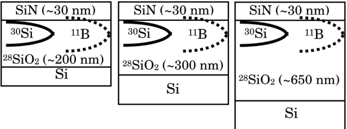
In order to investigate the effect of Si/SiO2 interfaces on boron diffusion in SiO2 , B and 30Si implanted samples were prepared as follows. The thermally grown28SiO2 layers of 200, 300, and 650 nm thicknesses were implanted with30Si at 50 keV to a dose of 2×1015 cm−2 and capped with a ∼30-nm-thick silicon nitride layer by rf magnetron sputtering.
Subsequently, the samples were implanted with 11B at 25 keV to a dose of 5×1013 cm−2. The final structures are shown in Fig. 2.4.
2.2 Annealing procedures
Annealing procedures employed in this study is as follow.
The samples grown on the 4-inch wafer were cut into 5×5 mm2 pieces, which enables us to use the same structures for different annealing conditions. Each piece was dipped in the solution consisted of H2O2 : H2SO4 at 1 : 3 for 5 min, followed by 5-min rinse using ion-exchanged water. This process was repeated twice for each sample. After drying, samples were placed on a quartz boat at the exit of a quartz tube located in a resistive
SiN (~30 nm)
Si
30
Si
11B SiN (~30 nm)
Si
30
Si
11B
SiN (~30 nm)
Si
30
Si
11B
28
SiO
2(~650 nm)
28
SiO
2(~300 nm)
28
SiO
2(~200 nm)
Figure 2.4: Sample structures of30Si- and B-implanted28SiO2 layers of 200, 300, and 650 nm thicknesses with SiN capping layers.
furnace. The furnace was prefired to stabilize at the target temperature. The boat was inserted into the quartz tube, where annealing ambient gas was flowing. Semiconductors processing grade quartz tubes and gas sources (argon and oxygen) were employed for maintaining the sample as clean as possible. After appropriate time of annealing, the boat was pulled to the edge of the quartz tube, whose temperature is room temperature. The sample temperature immediately went down to∼100◦C in flowing annealing ambient gas after pulling.
2.2.1 Annealing apparatuses
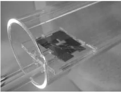
Figure 2.5 shows a picture of a quartz boat located at the edge of the quartz tube. The quartz boat was equipped with a port for inserting a thermocouple in order to measure accurately the sample temperature during thermal annealing. A well-calibrated ther- mocouple located in the clean quartz port was placed right next to the sample. The temperature was monitored and recorded automatically by PC throughout the course of annealing. The fluctuation of temperature was found to be less than ±2◦C.
Samples cut into 5×5 mm2 and cleaned were put on the boat. In order to prevent air from flowing in, a quartz cap was placed at the exit of a quartz tube, through which an semiconductor processing grade annealing ambient gas was flowing.
Before annealing, the quartz tube and boat were dipped in the solution (HF : HNO3
Figure 2.5: Picture of a quartz sample boat equipped with a port for inserting a thermo- couple. The boat, on which samples cut into 5×5 mm2 are put, is being inserted into the quartz tube.
= 1 : 3) for 5 min and were rinsed with ion-exchanged water for∼10 min to keep them as clean as possible. Then, they were dried in flowing semiconductor processing gas at room temperature, followed by degassing at 1250 ◦C.
After many high temperature annealing cycles, devitrification of the sample holder took place, and caused discrepancy of measured values of the diffusivity. In order to prevent the error due to the devitrification of the quartz holder, we used the simple isotope heterostructure as the reference samples to check the influence of the holder.
Fig. 2.6 shows a resistive furnace which was used for the diffusion annealing. The furnace can provide maximum temperature of 1500 ◦C.
2.2.2 Annealing conditions
The duration of annealing (diffusion time) was chosen so that it leads to diffusion length 2√
Dt=10-20 nm in order to retain a plateau of diffusion profile ofnatSiO2/28SiO2 isotope heterostructures in the natSiO2 layer. For each temperature, two periods of diffu- sion time have been employed.
For the annealing ambient, flowing argon with 1% oxygen was used. The oxygen was
Figure 2.6: Resistive furnace employed in this work.
mixed into argon in order to prevent SiO2 from decomposition, which tends to occur at higher temperatures and for lower oxygen partial pressures. This oxygen not only prevents decomposition but also oxidizes 28Si at the interface 28SiO2/28Si and forms additional
28SiO2. In order to decrease the rate of oxidation, the least amount of oxygen, which turns out to be 1%[28], needed for SiO2 to remain composed at 1300◦C was chosen.
Every time thermal annealing was conducted, a piece of Si substrate was annealed in the same furnace, and its oxide thickness was measured by ellipsometry in order to check the accuracy of temperature.
2.3 SIMS measurements
The depth profiles of30Si, B, and SiH(mass = 31) have been measured with ATOM- IKA SIMS 4000, which is equipped with a quadrupole mass spectrometer that analyzes secondary ions within a defined range of energy, using O+2 for a primary ion beam with acceleration energy 5 keV. An incident angle of the primary ion beam was 45◦. An elec- tron beam was irradiated during the measurement in order to prevent samples from charge accumulation. Crater depths resulted by sputtering were measured with a typical surface profilometer (Talystep of Taylor Hobson) with the accuracy of ± 10%. The main cause of the error in depth profiles determined by the SIMS measurements was the error of measurements of the crater depths. In order to minimize the error, we conducted SIMS measurements for each sample twice, and the reproducibility of SIMS measurements was always checked.
2.3.1 Insulator effects
The analysis of insulators using SIMS has traditionally been difficult because of the electrical charge buildup associated with the bombardment of the sample with a charged particle beam. The secondary ion energy distribution can be affected by charging of an insulating sample during analysis. Sample charging has the effect of producing an unknown offset on the sample and can move the energy distribution partially or even totally out of the energy window with the result that fewer or even no secondary ions are detected.
Many approaches have been attempted to reduce sample charging, but electron beam charge neutralization was applied at an early stage in instrument development and has proved to be most successful for almost every matrix attempted.
2.3.2 Surface effects
Several effects at the surface or in the near surface region must be accounted for to properly interpret data at the beginning of a depth profile.
A native oxide is present on many samples. In Si, a native oxide will begin forming almost immediately after a fresh surface is exposed and will reach a final thickness of 1 to 1.5 nm. For SIMS depth profiles, the surface oxide will cause a surface peak for many species.
Until the depth corresponding to the projected range of the primary beam has been eroded away by sputtering, the atom density of the primary species in the sample is not at equilibrium. The equilibration depth is related to the penetration of the primary species and increases with primary energy but decreases with angle of incidence from normal.
C and O present as surface contamination can require a significant depth of sputtering to be removed. As a result, much of the information in this part of the profile can be lost.
Other contaminants, such as Al, may be present at the surface and cause secondary ion yield changes or mass interferences.
Clean handling of the samples is very important. Samples that have dust often have contaminants that preclude the analysis of many important elements either directly or as the result of mass interferences.
An overview of diffusion in solids
In this chapter, an introduction to basics of diffusion in Si and SiO2 is given. In addition, this chapter introduces analyses of diffusion in the isotope heterostructures and implanted samples employed in this study.
3.1 Diffusion basics
Diffusion is the process by which matter is transported from one part of a system to another as a result of random microscopic (i.e., atomic-scale) motions [29, 30, 31], and the concentration of the matter is relaxed to its equilibrium concentraion.
3.1.1 Fick’s first law
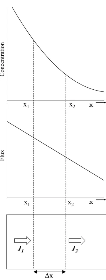
Fick established the mathematical model of diffusion in isotropic substances based on the hypothesis that the mass flux J, which is the rate of transfer per unit area, is proportional to the concentration gradient measured normal to the section, i.e.
J=−D∇C, (3.1)
whereCis the concentration of diffusing substance andDis called the diffusion coefficient.
The negative sign in eq. (3.1) arises because diffusion occurs in the direction to that of decreasing concentration.
14
x
Con c e n tr a ti on
x
F lu x
J
1J
2ǻ x
x
1x
2
x
2x
1Figure 3.1: (a) concentration and (b) flux of diffusing species as a function of position x.
Schematics of flux is shown in (c).
3.1.2 Fick’s second law
Unless a steady state exists, that is, the concentration at some point is changing with time, eq. (3.1) is still valid. In order to obtain more useful relation, we derive differential equations of diffusion in an isotropic substance from eq. (3.1) as follows. Mass conservation is a general physical constraint that may be imposed on diffusing systems.
Mass is conserved at all points in the medium, even under the action of a diffusion flux.
Thus the mass balance may be expressed as
accumulation rate = inflow−outflow. (3.2) Consider a bar of unit cross sectional area with thexaxis along its center. An element
∆x along the x axis has flux J1 to one side and J2 to the other, as shown in Fig. 3.1. If
∆x is very smallJ1 can be accurately described by
J1=J2−∆x
³∂J
∂x
´
. (3.3)
The volume of the element is 1·∆x (unit area times the thickness), so the net increase in matter in the element can be described by any part of
J1−J2 = ∆x
³∂C
∂t
´
=−∆x
³∂J
∂x
´
. (3.4)
Such procedure is done fory and z directions.
∆x∆y∆z
³∂C
∂t
´
=−∆x∆y∆z
³∂Jx
∂x +∂Jy
∂y +∂Jz
∂z
´
, (3.5)
or
∂C
∂t =−∇J. (3.6)
Substituting eq. (3.1) into eq. (3.6), we can obtain Fick’s second law:
∂C
∂t =−∇ ·¡
−D∇C¢
. (3.7)
If the diffusivity D is a constant, the divergence operator commutes only with ∇C, and eq. (3.7) simplifies to the linear form of Fick’s second law,
∂C
∂t =D∇2C. (3.8)
3.2 Diffusion in silicon
Atomic diffusion processes in silicon play an important role in the fabrication of elec- tronic devices in various areas. Silicon is one of the most important materials, and a considerable number of studies on diffusion in Si has been conducted, therefore, a signifi- cant progress has been made in understanding point defects and diffusion mechanisms in Si.
Boron doping is an important process in the fabrication of silicon based semiconductor devices. As dimensions shrink to nanometer scales, it becomes critical to obtain precise control of doping profiles. Therefore, a great deal of efforts is being devoted to under- standing and controlling diffusion of boron during implantation and annealing [32].
Elements diffusing in semiconductors are classified into slow or fast diffusers in relative manners [33]. Fast diffusers have diffusivity that is many orders magnitude larger than that of slow diffusers. The large difference between fast and slow diffusers is caused by the difference in different diffusion mechanisms, which are closely related to their incorporation in the lattice.
Slow diffusers, such as common group III and group V dopants, are substitutionally dissolved and require intrinsic point defects (vacancies and/or self-interstitials) for their diffusion process, while fast diffusers, such as Cu, Li, H, or Fe, are predominantly intersti- tially dissolved and move by jumping from one interstitial site to another interstitial site without any contribution of intrinsic point defects.
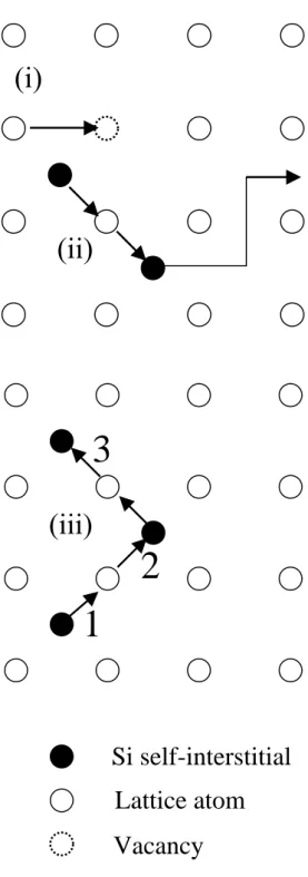
Figure 3.2 shows some common atomic diffusion models in a solid [33, 34], using a simplified two-dimensional crystal structure. At elevated temperatures the lattice atoms vibrate around the equilibrium lattice sites. Occasionally a host atom acquires sufficient energy to leave the lattice site, becoming a self-interstitial and creating a vacancy. When a neighboring atom migrates to the vacancy site, it is called vacancy mechanism, as schemat- ically shown in Fig. 3.2(a).
Suppose elements A are placed at interstitial (Ai) and substitutional (As) sites. Kick- out mechanism involves self-interstitial (I) for interchanging between (Ai) and (As) via the reaction
Ai↔As+ I, (3.9)
as shown in Fig. 3.2(a).
In the interstitialcy mechanism, a self-interstitial replaces a substitutional atom which
(i)
(ii)
1
2 3
Si self-interstitial Lattice atom Vacancy
(iii)
Figure 3.2: Models of atomic diffusion for a two-dimensional lattice. (i) Vacancy, (ii) kick-out, and (iii) interstitialcy mechanisms.
then in return replaces a neighboring lattice atom, as shown in Fig. 3.2(b).
3.2.1 Silicon self-diffusion in silicon
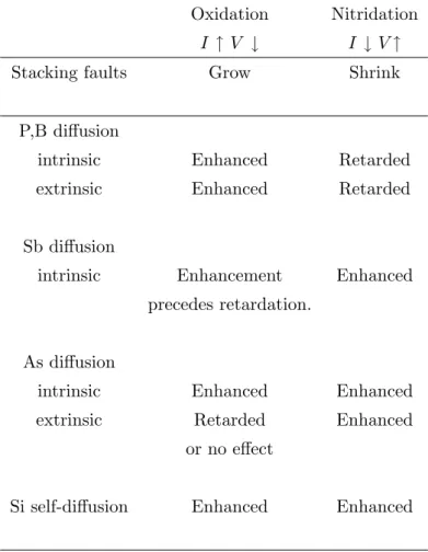
Silicon is a host atom in crystalline silicon, therefore, Si self-diffusion has to be me- diated by point diffects. Ural et al., reported that Si self-diffusion in crystalline silicon is enhanced during nitridation and oxidation[35], as shown in table. 3.1. Therefore, it is known that Si self-diffusion in Si involves self-interstitials and vacancies. In addition, it was reported that Si diffuses in Si via direct exchange mechanism [36]. However, it is generally thought that the contribution of the direct exchange mechanism is very small.
Table 3.1: Summary on oxidation and nitridation effect on stacking fault and diffusion behaviors. (see ref. 32 for detail)
Oxidation Nitridation I ↑ V ↓ I ↓V↑
Stacking faults Grow Shrink
P,B diffusion
intrinsic Enhanced Retarded
extrinsic Enhanced Retarded
Sb diffusion
intrinsic Enhancement Enhanced
precedes retardation.
As diffusion
intrinsic Enhanced Enhanced
extrinsic Retarded Enhanced
or no effect
Si self-diffusion Enhanced Enhanced
3.2.2 Boron diffusion in silicon
As mentioned above, boron is one of group III dopants and is dissolved almost entirely on substitutional sites. Therefore, boron diffusion is mediated by intrinsic point defects.
Boron diffusion is retarded during nitridation and enhanced during oxidation[37], as shown in table 3.1. Moreover boron diffusion mainly involves self-interstitials [38].
B diffusion is known to be retarded by nitridation [39, 40], which induces vacancy su- persaturation. Using the degree of retardation, the fractional diffusion component related to self-interstitials fI of B has been estimated to be close to unity [39]. In addition, due to the Fermi level effect, doping with p-type impurities increases the equilibrium concen- tration of self-interstitials, while it decreases that of vacancies [41]. In the extrinsic region of B profiles, therefore, the vacancy contribution is very minor because the self-interstitial and the vacancy contribution to the Si self-diffusion under intrinsic conditions [39] are close to each other. In the intrinsic region, the supersaturation of self-interstitials induced by the kick-out reaction:
Bi ↔Bs+I, (3.10)
induces an undersaturation of vacancies, and hence the vacancy contribution is again smaller than the interstitial contribution. This minor contribution of vacancies compared to that of self-interstitials in both the extrinsic and intrinsic regions retards both the Frank- Turnbull [33, 41] and the vacancy mechanisms. Consequently, B diffusion is primarily governed by the kick-out mechanism.
3.2.3 Diffusion during oxidation of silicon
Oxidation of silicon is one of the most important processes in fabrication of Si based electronic devices. Therefore, a considerable number of studies on oxidation of silicon has been reported. It is known that oxidation of Si leads to enhanced diffusion of the common substitutionally dissolved B, In, Al, Ga, P, As, and Si, and to nucleation and growth of interstitial-type dislocation loops containing stacking faults (oxidation-induced stacking faults: OSF). These phenomena can be explained by self-interstitials injection into Si substrate from the Si/SiO2 interface during thermal oxidation. Injection of self- interstitials leads to supersaturation of self-interstitials. Therefore, diffusion of atoms which are mediated by silicon self-interstitials is enhanced, and oxidation-induced stacking faults are grown during thermal oxidation.
Table 3.1 summarizes some of the results from oxygen and NH3 treatments on the dif- fusion, including the growth or shrinkage of oxidation-induced stacking faults (OSF).The NH3ambient is known to inject vacancies and lead to an undersaturation of self-interstitials.
Therefore, diffusion involving interstitials is retarded and stacking faults shrink.
The driving force for self-interstitial injection during oxidation is the volume expansion of about a factor of two associated with the SiO2 formation at the SiO2/Si interface.
No vacancies have to be involved for understanding oxidation-enhanced diffusion (OED).
The explanation of the observed oxidation-retarded diffusion (ORD) of Sb under the same oxidation-conditions requires the presence of a second type of point defects. The simul- taneous occurrence of retarded and enhanced diffusion phenomena can be explained by a model which assumes that Sb diffuses predominantly via vacancies but oxidation-induced self-interstitials partly recombine with vacancies according to
I + V↔0, (3.11)
where 0 denotes the undisturbed lattice. Under thermal equilibrium conditions vacancies and self-interstitials will possess their equilibrium concentrations CeqV and CeqI , respec- tively. If the local dynamical equilibrium is established, this process leads to an under- saturation of vacancies (CV<CeqV) associated with a supersaturation of self-interstitials (CI>CeqI ) via mass action law
CVCI= CeqVCeqI . (3.12)
In eq.(3.12), CV and CI are the concentrations of vacancies and self-interstitials, respec- tively. For a quantitative treatment, the diffusivity D under thermal equilibrium condi- tions for intrinsic point defects (CV= CeqV, CI= CeqI ) is expressed in terms of a diffusion component DI involving self-interstitials and a diffusion componentDV via vacancies:
Deq=DI+DV. (3.13)
For non-equilibrium conditions Dchanges to D=DICI
CIeq +DVCV
CVeq. (3.14)
3.3 Diffusion in SiO
23.3.1 Point defects in SiO2
Compositional and structural transition layers exist between bulk SiO2 and crystalline Si substrate. In addition, stoichiometric bulk SiO2 possesses a variety of point defects [42, 43]. The dangling orbital or paramagnetic centers have been the subjects of extensive research in thermal SiO2 as well as crystalline silica. Electron spin resonance (ESR) is the powerful tool for study of these centers.
The Pb center, corresponding to an unpaired Si-electron or Si-dangling bond, is char- acteristic of the SiO2/Si interface.
The excess-oxygen center, called non-bridging-oxygen hole center (NBOHC), i.e., O3 ≡Si−O·. . .H−O−Si≡O3 and the peroxy radical (O3 ≡Si−O−O·) are impor- tant centers. They do not exist in quartz, since they would require a severe local distortion of the lattice.
The essential element of the very important E’ center is the moiety (O3 ≡Si·). There are two main subtypes, i.e., E’γ (O3 ≡Si·. . .+Si≡O3) and E’s (O3 ≡Si·). They have been most often and most clearly observed.
3.3.2 Diffusion in SiO2
Oxygen diffusion in SiO2 is a great importance in thermal oxidation of silicon. There- fore, extensive studies have been given to oxygen diffusion in SiO2[44, 45]. It was reported that oxygen diffusion has two different, parallel and probably non-correlated diffusion mechanisms [46]. In one of them, oxygen is transported through the oxide network with- out interacting with it. In the other, oxygen is incorporated in the near-surface region, mostly by exchange for oxygen atoms from the near-surface oxide network via interstitialcy mechanism [46].
Boron diffusion in SiO2 is also important for device fabrication process. Fair reported that boron diffusion is mediated by peroxy-linkage defects (O3 ≡Si−O−O−Si≡O3) [47]. Otani et al. reported first-principle total-energy calculations that provide stable and metastable geometries and diffusion mechanisms of boron in SiO2 with point defects which contain O vacancies and O interstitials, and found that a boron atom forms various (meta)stable geometries in SiO2 with point defects, depending on its charge state [21, 22, 23].
3.4 Analysis of diffusion profiles
This section describes the solutions which will be used in the later chapters to analyze our experimental results.
3.4.1 Instantaneous planar diffusion source in an infinite medium Let us consider the problem of instantaneously releasing a quantity of diffuser M, at the plane x = 0 at t = 0, as shown in Fig. 3.3. The diffuser is allowed to spread into the two adjacent material occupying the half-spaces 0 < x < ∞and −∞< x <0. Both materials have equal and constant diffusivities,D. For example, this situation corresponds to delta doping of impurity atoms in semiconductors.
Application of the Laplace transform procedure to Fick’s second law (eq. (3.3)) yields;
Z ∞
0
exp(−pt)∂2C
∂x2dt− 1 D
Z ∞
0
exp(−pt)∂C
∂t dt= 0. (3.15)
The first integral appearing in eq.(3.15) may be determined by transposing the order of the differentiation and integration:
Z ∞
0
exp(−pt)∂2C
∂x2dt= ∂2
∂x2 Z ∞
0
Cexp(−pt)dt= d2C˜
dx2, (3.16)
where the image function ˜C produced on the right-hand side of eq. (3.16) is the Laplace transform of the concentration field, defined operationally by the integral
C˜≡ Z ∞
0
Cexp(−pt)dt. (3.17)
The second integral in eq. (3.15) arising in the transform procedure for Fick’s second law can be evaluated by using partial integration
0 x
M t=0
Figure 3.3: Flow of an instantaneous source M released into surrounding semi-infinite media.
Z ∞
0
exp(−pt)∂C
∂t dt=
"
C(x, t) exp(−pt)
#∞
0
−p Z ∞
0
−C(x, t) exp(−pt)dt
= 0−C(x,0) +pC.˜
(3.18)
Equations (3.16) and (3.18) are inserted into eq. (3.15), and we can obtain an ordinary deferential equation (ODE)
p
DC(x, p)−d2C(x, p)
dx2 = C(x,0)
D , (3.19)
subjects to the initial condition at time t=0, C(x,0)=0 for all x 6= 0 and the boundary condition C(±∞,t)=0, so the finite mass of diffuserM released by the source cannot alter the composition of this infinitely long bar of material far away from the source’s location.
The diffusion process is overall subject to the integral mass constraint Z ∞
−∞
C(x, t)dx=M, (3.20)
which accounts for the diffuser spreading with time over all space. The initial condition reduces the Laplace-transformed Fick’s second law
p
DC(x, p)−d2C(x, p)
dx2 = 0, (3.21)
since the right-hand side of eq. (3.19) vanishes at t = 0 for all x, except for the source plane itself at x= 0. Now eq. (3.21) is a well-known ODE, and the solution of this ODE is
C˜=Aexp
³rp Dx
´
+Bexp
³
− rp
Dx
´
. (3.22)
The boundary condition specified above indicates that both terms appearing in the eq. (3.22) will be needed to provide solutions for the left- and right-going diffusion fields. Therefore, the right-going diffusion field is
C˜=Bexp
³
− rp
Dx
´
, x >0 (A= 0), (3.23) and the left-going diffusion field is
C˜ =Aexp
³rp Dx
´
, x >0 (B = 0). (3.24)
Symmetry requires that diffusion flow left and right equally, so the global mass constraint for the half-spacex >0 can be formulated by eq. (3.23) into eq. (3.20) as
Z ∞
0
C(x, t)dx= M
2 . (3.25)
Now, applying the Laplace transform to eq. (3.25), we obtain L
(Z ∞
0
C(x, t)dx )
= L (
M 2
)
(3.26)
or Z ∞
0
e−pt Z ∞
0
C(x, t)dxdt= Z ∞
0
e−ptM
2 dt. (3.27)
From eq. (3.27), we obtain the expression for the image function Z ∞
0
C(x, p)dx˜ = M
2p. (3.28)
Now, substituting eq. (3.23) into the left-hand side of eq. (3.28) for x >0 shows that Z ∞
0
Bexp
³
− rp
Dx
´
dx= M
2p (3.29)
and "
− B pp/Dexp
³
− rp
Dx
´#∞
0
= M
2p. (3.30)
Solving eq. (3.30) for B gives
B= M 2√
pD. (3.31)
Substituting eq.(3.31) into eq. (3.29) gives the transform solution, C(x, p) =˜ M
2√ D
exp
³
−√x
D
√p
´
√p . (3.32)
The transform solution can be inverted to find the concentration fieldC(x, t):
L−1{C}˜ =C(x, t) = M 2√
DL−1 (
e−a√p
√p )
(3.33) where a= √x
D.
Reffering to the table of Laplace transforms, we use the following relation:
L−1 (
e−a√p
√p )
= 1
√πtexp Ã
−a2 4t
!
(3.34) to obtain the diffusion solution:
C(x, t) = M 2√
πDtexp Ã
− x2 4Dt
!
. (3.35)
C(x,0)=C
SC(x,0)=C
SC(x,0)=C
C-h 0 h
C
CC(x,0)
C
sFigure 3.4: Configuration of a composite slab and the concentration as a function of x.
3.4.2 Solution for isotope heterostructures
In this section, the solution of Fick’s second law for isotope hetero structures will be given. The linearity of the diffusion equation permits the use of superposition to produce new solutions for different geometric arrangements of the sources. A basic solution found for the release of an instantaneous amount of diffusers from a planar source into an infinite system, can be superposed to develop new solutions. This procedure requires that the boundary conditions for the new solutions are identical to those for the basic solution.
Now, consider the semi-infinite system as shown in Fig. 3.4. A slab of width 2hhaving a uniform initial concentrationCcis joined as two long bars having a uniform concentration Cs. The central slab and the long bars are the same phase and have equal diffusivities.
The initial concentration may be interpreted as a continuous distribution of instantaneous, differential, planar sources of strengthdM =CcdˆxanddM =Csdˆx, spread uniformly over the central slab and both side bars, respectively.
The concentration response at any location −∞ < x <∞, at any future time t >0, is the unknown field C(x, t). This concentration field may be thought of as the sum, or integral, of all the sources released instantaneously at t = 0, from locations −∞ < x <ˆ
∞. The total response occurring at any plane x at some later time t is given by the superposition, or source integral,
C(x, t) =Cs Z −h
−∞
exp(−(x−ˆ4Dtx)2)
√4πDt dˆx+Cc Z h
−h
exp(−(x−ˆ4Dtx)2)
√4πDt dˆx +Cs
Z ∞
h
exp(−(x−ˆ4Dtx)2)
√4πDt dˆx.
(3.36)
The integrand of the superposition integral corresponds to the instantaneous source solu- tion as described by
C(x, t) = M 2√
πDtexp
³
− x2 4Dt
´
. (3.37)
Equation (3.36) is evaluated using the variable substitution u= x−xˆ
2√
Dt. (3.38)
The total differential ofu is
du= −dˆx 2√
Dt (x= const). (3.39)
The source integral, eq. (3.36), may be written in terms of the new variableu(ˆx, t) as
C(x, t) = Cs
√π Z x+h
2√ Dt
∞
−e−u2du+ Cc
√π Z x−h
2√ Dt x+h 2√
Dt
−e−u2du+ Cs
√π Z −∞
x−h 2√
Dt
−e−u2du
=−Cs
√π
"Z x+h
2√ Dt
0
e−u2du− Z ∞
0
e−u2du
#
− Cc
√π
"Z x−h
2√ Dt
0
e−u2du− Z x+h
2√ Dt
0
e−u2du
#
− Cs
√π
"Z −∞
0
e−u2du− Z x−h
2√ Dt
0
e−u2du
#
=−Cs 2
"
erf Ã
x+h 2√
Dt
!
−erf Ã
∞
!#
−Cc 2
"
erf Ã
x−h 2√
Dt
!
−erf Ã
x+h 2√
Dt
!#
−Cs 2
"
erf Ã
−∞
!
−erf Ã
x−h 2√
Dt
!#
,
(3.40) where erf(z) is the error function as defined by
erf(z) = 2
√π Z z
0
exp
³
−η2
´
dη. (3.41)
Then we can obtain the solution of Fick’s second law for this problem as described by C(x, t) =Cs+Cc−Cs
2
"
erf Ã
x+h 2√
Dt
!
−erf Ã
x−h 2√
Dt
!#
. (3.42)
For this solution it is assumed that the medium, which diffusion takes place in, is infinitely long. Since ∂C∂x = 0 at x = 0 in this solution, it can be used for the isotope heterostructure shown in Fig. 2.1.
C(x) =C28SiO2 +CnatSiO2−C28SiO2 2
"
erf
µx+h 2√
Dt
¶
−erf
µx−h 2√
Dt
¶#
. (3.43)
3.4.3 Analysis of ion-implanted samples
Each implanted ion has a random path as it moves through the target, losing energy by nuclear and electronic stopping. The depth distribution of ions can be approximated as Gaussian with standard deviation σp. Far from a mask edge, we can neglect lateral motion and approximately write the implanted ion concentration C(x) as
C(x) =C0exp
Ã−(x−Rp)2 2σp2
!
, (3.44)
where Rp is the average depth of the implanted ions and called the projected range, and C0 is the peak concentration. If the total dose is Φ, then theC0 is expressed by
C0 = Φ
√2πσp. (3.45)
One may notice that eq. (3.44) is equivalent to eq. (3.37), which is the solution for the instantaneous diffusion source. If after t1, the diffusion profile is identical with the initial distribution of implanted ions, described as
C(x,0) =C0exp Ã
−(x−Rp)2 2σp2
!
= M
2√
πDt1exp
³
−(x−Rp)2 4Dt1
´
, (3.46)
the distribution of implanted ions after t is the same distribution as the instantaneous diffusion source after t+t1. Therefore, the diffused distribution of implanted ionsC(x, t) is given by
C(x, t) = M 2p
πD(t1+t)exp
³
−(x−Rp)2 4D(t1+t)
´
. (3.47)
![Figure 1.1: The schematic view of MOS structure [1]. The gate electrode is usually highly boron doped poly silicon.](https://thumb-ap.123doks.com/thumbv2/123deta/6080332.2080915/9.892.175.721.749.977/figure-schematic-structure-electrode-usually-highly-boron-silicon.webp)
![Table 1.1: Roadmap of technology node, gate length, and equivalent oxide thickness [8].](https://thumb-ap.123doks.com/thumbv2/123deta/6080332.2080915/11.892.148.746.944.1059/table-roadmap-technology-node-length-equivalent-oxide-thickness.webp)