Abstract
Electron beam lithography (EBL) is expected to achieve the formation of very fine dot arrays for bit-patterned media applications due to its resolution capability and placement accuracy. However, the resolution-limiting factors of electron beam lithography (EBL) at the sub-10 nm length scale are not well understood, which has limited our ability to further improve its resolution. Therefore, using the simulation method to analyze the limiting factors of EBL for sub-10 nm patterning is necessary to be done.
In order to revealing the limiting factors of high resolution patterning, I focused my study on two main aspects. The first was evaluating the dependence of exposure conditions (such as incident beam energy, resist thickness, resist type, etc.) to reduce the electron beam scattering range. The second aspect was estimating resist profiles with solubility rates based on various developers to determine optimal development contrast. The details of the two aspects were described as follows.
The first aspect: Roughly evaluation of the resist profile estimated by critical energy deposition based on energy deposition distribution (EDD)
1) A home-made Monte Carlo simulation of electron-atom scattering was made.
2) The energy deposition distribution was calculated in thin resist layer on Si substrate.
3) The estimation of nano-sized dot arrays based on critical deposited energy in a parameter of incident electron energy, electron beam diameter, resist thickness and resist type were studied.
4) High incident energy beam, small sized Gaussian beam, thin resist film, negative resist were demonstrated that there are benefit to reduce electron beam scattering range and form very fine nano-sized pattern.
The second aspect: Precise estimation of HSQ resist profiles by using various developers with different contrast
1) A new development model of calculating resist profiles with solubility rates based on the three-dimensional EDD was proposed.
2) A sharpened nano-dot resist pattern was obtained by selecting a suitable EDD region. 3) The calculated resist profiles by using the new model agrees well with the experiment
results.
4) The effects of exposure dosage and solubility rate on contrast of developer were studied. The resist profiles with various contrast developers (𝛾 from 12 to 1) were calculated. We demonstrated that small dosage interval (∆𝐸𝐷𝐷) is an important parameter to improve the resolution.
5) The suitable contrast of developers was determined by evaluating the predicted resist profiles. High contrast developer was effective to form very fine dot pattern with sufficient. 6) The exposure allowance for high contrast resist and low contrast resist was investigated. We demonstrated that high contrast resist has small exposure allowance. It indicted that we should control exposure dosage severely by using high contrast resist for high resolution patterning.
As described above, EB exposure and development calculation is demonstrated to obtain very fine resist profile using high energy electron high contrast developer and negative resist. This indicates that the optimal condition of EB lithography opens new era to control nanometer-sized structures.
要旨
電子線描画法は高分解能かつ位置精度が正確であるため、パターンドメディア技 術のための微小ドット形成方法として有望視されている。しかし、sub-10 nm におけ る電子線描画の解像度の限界について、現像プロセスまで含めた電子線描画法が殆ど 研究されていないのが現状である。本研究においては、現像プロセスまで含めた電子 線描画法をシミュレートすることにより、電子線描画法による微細化技術の限界を検 討した。 本研究では、電子線描画法による微小パターン形成に与える要因を分析するため、 以下の二つの研究を行った。一つは電子散乱領域を抑えるため、様々な露光条件の依 存性(例:入射ビームのエネルギー、レジストの厚さ、レジストの種類など)につい て検討した。もう一つは、種々のコントラストを持つ現像液がパターンの形成に与え る影響の分析である。これにより、各種コントラストを持つ現像液によるパターン形 状の予測を行い、最適なコントラストを予測した。これら二つの研究の概要は以下の 通りである。 1、3 次元エネルギー堆積密度(EDD)に基づき、閾値エネルギーによる、レジスト プロファイルのラフな評価 1)ホームメード電子散乱のモンテカルロシミュレーションを構築した。 2)レジスト中で堆積したエネルギーの 3 次元密度分布を計算した。 3)上記エネルギー堆積密度に基づき、それぞれの露光条件(入射ビームのエネルギ ー、レジストの厚さ、レジストの種類など)において、形成されるナノドットの 形状を予測した。 4)高エネルギー入射ビーム、微小ビーム径、薄膜レジスト、ネガティブレジストを 用いることにより電子散乱領域を抑え、微小ナノドット列形成に有効であること を証明した。 2、各種コントラストの現像液における HSQ レジストプロファイルの正確な予測 1)実験の露光量と溶解速率に基づき、レジスト中の蓄積したエネルギーの分布によ り、レジストプロフアイルの計算ために新たな現像モデルを提案し、構築した。 2)最適なエネルギー領域を選択することにより、最適な微小ドットパターン(約 7nm 径)が形成できることが分かった。3) 提案モデルで計算したレジストプロファイルは実験の結果と一致していること を示し、提案モデルがパターンプロフアイルの予測に有効であることを証明した。 4)露光量による溶解速度特性に基づいた 3 次元エネルギー蓄積分布と現像作用の関 係を見出し、各種コントラストを持つ現像液がレジストプロファイルに与える影 響を検討した。 5)計算したレジストプロファイルを評価することによって、微小パターンの形成に は現像液の最適なコントラスト値を選択することが重要であることが分かった。 コントラストが高い現像液は微小パターンの形成に有利であることが分かった。 6)コントラストが高い現像液は狭い露光許容量を持ち、反対にコントラストが低い 場合は広い許容量がある。コントラストが高い現像液を用いる時には露光量を細 かく制御する必要があることが分かった。 上記のように、電子線描画と現像過程のシミュレーションによって、高エネルギ ーの電子線、高コントラスト現像液、ネガティブレジストを用いることが、微小なパ ターンを形成するのに有効であることを明らかにした。実験において、電子線描画の 最適な条件を見出すことにより、ナノメートル構造を制御することが可能になると予 測される。
Table of Contents
Abstract ... I List of Symbols ... IX Acknowledgments ... XI Chapter 1 Introduction ... 1 1.1 Background ... 11.2 The Purpose and Content of the Work ... 4
1.3 The Outline of the Research ... 6
References ... 8
Chapter 2 Electron Beam Lithography ... 10
2.1 Nanolithography ... 10
2.2 Electron Beam Lithography ... 11
2.3 Electron-Solid Interactions ... 12
2.4 Electron Beam Resist ... 13
2.4.1 Positive resist ... 14
2.4.2 Negative resist ... 15
2.5 Development Process ... 16
2.6 Conclusions ... 17
References ... 18
Chapter 3 Monte Carlo Simulations of Electron Scattering in Solid for Electron Beam Lithography ... 19
3.1Elastic Scattering ... 20
3.1.1 Basics ... 20
3.1.2 Rutherford cross section ... 20
3.1.3 Mott cross section ... 21
3.3Monte Carlo Modeling ... 23
3.3.1 Multiple scattering model ... 23
3.3.2 Single Scattering Model ... 24
3.3.3 Hybrid model ... 24
3.4 Modeling of Electron Scattering Process ... 25
3.4.1 Determination of scattering center in polybasic material ... 26
3.4.2 Multilayer system ... 27
3.4.3 Calculation of trajectories of primary electron in scattering process ... 28
3.4.4 Calculation of Electron Deposition Distribution in resist film ... 29
3.5 Application of Monte Carlo simulation ... 29
3.5.1 Positive resist (PMMA resist) ... 29
3.5.1.1 Description of electron scattering trajectories ... 30
3.5.1.2 Energy deposition distribution (EDD) ... 31
3.5.1.3 Consideration for resist development based on the EDD ... 32
3.5.2 Negative resist (Calixarene resist) ... 34
3.5.2.1 Electron scattering trajectories in thin Calixarene resist ... 34
3.5.2.2 Energy deposition distribution in Calixarene resist ... 35
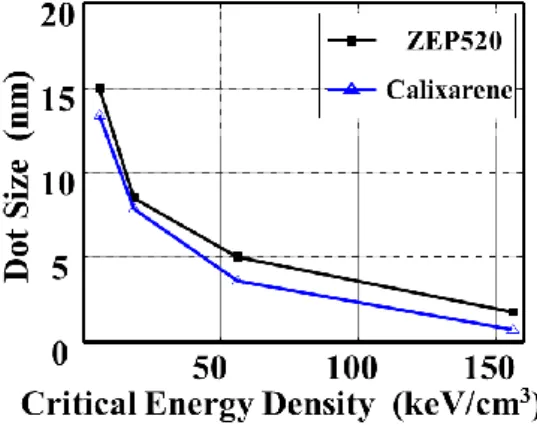
3.5.3 Comparison of Calixarene and ZEP520 resists using their EDD ... 36
3.5.3.1 Energy deposition distribution in Calixarene and ZEP520 resists ... 36
3.5.3.2 Relationship between dot size and critical energy for development ... 37
3.5.3.3 Consideration for resist development based on the EDD ... 39
3.5.3.4 Consideration of the different limitations in ZEP520 and Calixarene resists ... 41
3.6 Conclusions ... 42
References ... 43
Chapter 4 Dependence of Electron Beam Diameter, Electron Energy, Resist Thickness and Resist Type for Forming Nano-sized Dot Arrays in EB Lithography ... 45
4.1 Beam Diameter Dependence ... 46
4.1.2 Effect of beam diameter on nano-sized-formation ... 46
4.2 The Dependence of Incident Electron Energy... 49
4.3 Dependence of Thickness of Resist... 50
4.4 Dependence of Critical Energy ... 52
4.5 Comparison of Calixarene Resist with PMMA Resist ... 54
4.6 Conclusions ... 55
References ... 56
Chapter 5 New Simulation Model for Developing Resist Pattern Based on EDD in EBL ... 57
5.1 Modeling of Resist Development in EB Drawing ... 58
5.1.1 EDD calculation ... 58
5.1.2 Resist development model ... 60
5.2 Verification of the New Model ... 62
5.3 Conclusions ... 66
References ... 67
Chapter 6 Estimation of HSQ Resist Profile by Enhancing Contrast for High Resolution Lithography ... 69
6.1 High Contrast of Developers for Nano-sized Patterning ... 70
6.1.1 Definition of contrast parameter in developing ... 70
6.1.2 Relationship between exposure dose D and EDD ... 71
6.1.3 The ∆EDD used in the simulation... 72
6.1.4 Calculating optimal resist profile based on EDD ... 73
6.2 Relationship between Contrast and Allowance of Optimal Exposure for High contrast patterning ... 75
6.2.1 Method of calculating the exposure allowance ... 76
6.2.2 Calculating the allowance for high contrast resist patterning ... 76
6.2.2.1 The allowance of high contrast resist ... 77
6.3 Calculating the Resist Profiles with Various Contrast Developers used in Experiments ... 80
6.3.1 Measurement of development contrast curve ... 80
6.3.2 Contrast curve ... 80
6.3.3 Determining the suitable EDD regions ... 81
6.3.4 Calculating resist profiles with various developers ... 82
6.4 Developers for 15×15 nm2 Pitched Dot Arrays ... 83
6.5 Conclusions ... 85
References ... 86
Chapter 7 Summary and Future Work ... 88
7.1 Summary ... 88
7.2 Future Works ... 90
List of Related Papers ... 91
List of Symbols
Z Atomic number of target atom, 23e Electronic charge, 23 r0 Screening radius, 23
a0 Bohr‟s radius, 23 𝛼 Screening factor, 23
𝜎𝑒 Rutherford cross section, 23
n Number of atoms in a unit volume, 24 NA Avogadro‟s number, 24 𝜌 Density, 24 A Atomic weight, 24 E Energy of electron, 27 𝜃 Scattering angle, 27 𝜙 Scattering angle, 27 ℎ Plack‟s constant, 27 p Electron momentum, 27
R Uniform random number between 0 and 1, 28 R1 Uniform random number between 0 and 1, 28
R2 Uniform random number between 0 and 1, 28
Ji Mean ionization energy of atom I, 28
𝑆𝑛 Step length between (n-1)th and nth scatterings, 28 |𝑑𝐸/𝑑𝑠|𝐸𝑛 Mean energy loss, 28
𝑃𝑖 Probability of scattering off an atom of the i-th element, 29
Ec Stopping energy, 31 ∆𝑉 The ring volume, 32 ∆𝑧 Thickness of sub-layer, 32 ∆ Increment in radius direction, 32 𝑁0 Total number of incident electron, 32
𝜎 Standard deviation, 50
P Uniform random number between 0 and 1, 50
𝐷( 𝑧) Energy deposition as a function of the radial distance and vertical distance 𝑧, 67
𝑣𝑟, 𝑣𝑧 Solubility rates in the radial and vertical directions, respectively, 67 𝛾 Contrast value, 68
R Experimental residual resist thickness, 68
0 Original resist thickness, 68
t Development time, 68
∆ Step time, 69 EB Electron beam, I
EBL Electron beam lithography, I EDD Energy deposition distribution, I BPM Bit pattern media, 2
FIB Focused ion beam lithography, 3 NIL Nano imprint lithography, 3 HSQ Hydrogen silseqioxene resist, 4 EID Energy intensity distribution, 5 PEB Post-exposure-bake, 11
PMMA Poly(methyl methacrylate), 16 PBS PolyButene-1-Sulfone, 16
EBR-9 A copolymer of trifluoroethyl a-chloroacrylate and tetrafluropropyl a-chloroacrylate, 16
ZEP A copolymer of chloromethacrylate and methylstyrene, 16 TMAH Tetramethylammonium hydroxide, 17
CMC6 p-chloromethyl-methoxy-calix[6]arene, 39 CMC4 p-chloromethyl- methoxy- calix[4]arene, 39 SEM Scanning electron microscope, 50
∆EDD EDD interval between the initial EDD for minimum solubility rate and the full EDD for maximum solubility rate, 8
Acknowledgments
I would like to express my gratitude to my supervisor, Prof. S. Hosaka for giving me the opportunity to study in the Hosaka Laboratory of Guma University and for bringing me to get to know the EB-lithography for forming nano-scaled dot arrays. Your invaluable supervision and constant supports throughout the 3 years doctoral course of my study helped me to overcome difficulties and achieved the goals in my research works. Importantly, studying in your high quality and good environmental research group gives me a good opportunity to a professional career in the field of nanotechnology.
I would like to thank Assistant Prof. Y. Yin. He really supported me with patience and understanding during this experience. I would also like to thank all the members of our research group: Mr. T. Komori, Dr. T. Tamura, Dr. Z. Mohamad, Dr. M. Huda, and Ms. J. Liu. I especially would like to thank Mr. T. Komori for giving me the experimental results to support my simulation program which is one of the essential parts of the research. I also would like to acknowledge the Japanese Government (JASSO) for a financial support for my study.
Finally, I would like to thank my parents and my husband for their tireless support and encouragement from the beginning until the completion of my PhD program.
Chapter 1 Introduction
1.1 Background
Magnetic recording, invented over 100 years ago, has played a key role in the development of information storage technologies, including analog audio, video and digital data recording. Since the scale of the first magnetic hard disk drive by IBM in 1956, the capacity and storage density, i.e. the number of bits per square inch (bits/in.2), have increased dramatically. The density will exceed 1 Tbit/in.2 with a couple of years (Fig. 1.1) 1-3.
Data is stored in circular tracks on a disk shown in Fig. 1.2 4. Within each track, a stream of data bits is recorded as regions of opposite magnetization. Each track consists of equally spaced bit cells, with a digital „1‟ being indicated by a boundary (called a magnetic transition) between regions of opposite magnetization within a bit cell, and a „0‟ being indicated by a continuous regions without such a boundary 4. In each bit cell, there are many tiny magnetic grains. These grains are randomly created during the deposition of the magnetic film. Each grain behaves like an independent magnet whose magnetization can be flipped by the write head during the data writing process.
As the recording density increases, making smaller grains is necessary to be done to satisfy the progress of information technology. However, if the grain size becomes so small that further shrinkage would cause the magnetization of the individual grains to be unstable. The magnetic anisotropy energy of the grain becomes small compared to the thermal fluctuation energy at room temperature. 2 If the magnetic anisotropy falls below a certain value, the magnetization of the grain can flip spontaneously. If a significant fraction of the grains on the disk flip spontaneously, the data stored on the disk will erase itself. Thermal
fluctuation can be reduced by using material with high magnetic anisotropy energy. However, the reversal field becomes too high compared to the capability of current recording head material.
Bit pattern media (BPM) as a promising approach has been proposed that it can overcome the problem of thermal instability 5-7
. With patterned media, the magnetic layer is created as an ordered array of highly uniform islands, each island capable of storing an individual bit as shown in Fig.1.3. Since each island is a single magnetic domain, patterned media is thermally stable, even at densities far higher than that can be achieved with conventional media. 4 There is a report that put forward by Hitachi Corporation 4 (shown in Fig. 1.4). If the recording density of 100 Gbit/in.2, the islands need to have a center-to-center spacing of 86 nm. To move to 1 Tbit/in.2, a spacing of 25 nm is needed. At 10 Tbit/in.2, this spacing is just only 7.9 nm. Therefore, in order to utilize the patterned media technique to increase the data recording density, it is important to develop a way to form very fine patterns at first.
Fig.1.2 The schematic diagram of conventional media recording (HGST Corporation) 4.
Fig.1.3 Schematic diagram of bit patterned media recording (HGST Corporation) 4.
Electron beam lithography (EBL) 8, focused ion beam (FIB) lithography 9, and nano imprint lithography (NIL) 10 are currently the three most widely employed nano-lithography techniques. Unlike NIL, EBL can generate arbitrary patterns without the need of fabricating a mold first. Though not as versatile as FIB, which can do both lithography using a resist and milling, EBL is capable of drawing finely controlled pattern to resist without ion contamination 11. Therefore, EBL is expected to allow the formation of very fine pitch or dot arrays with high resolution for patterned media with high density recording 12.
Using EBL, many researches of fabricating sub-10-nm dot arrays with various resists have been put forward. Calixarene has been studied as a candidate resist for fabricating very fine dot arrays with a 25 nm pitch using a 30 keV accelerating voltage. EB drawing using Calixarene resist promises to open the way toward ultrahigh-density recording at 1.6 Tbits/in.2 (corresponding to a dot array of 20-nm period) using very thin (less than 20 nm) film 10-11. In recent, hydrogen silsesqioxene (HSQ) resist probably attracted more attention than other negative resists 12-13. HSQ as an excellent inorganic EBL resist that has demonstrated the highest resolution of 9-nm period line array patterns due to its small molecular size 14. Furthermore, many efforts have been made to improve the density of BPM by using new EBLs and new developments. For example, 12-nm-pitch HSQ dot arrays were fabricated by Yang et.al. 15 using 100 keV exposures combined with high concentration and high temperature development, and 9-nm-pitch HSQ nested “L” structures were fabricated by using a Raith 150 system at 30 keV combined with high contrast salty development 16. However, the resolution limiting factors of EBL at the sub-10-nm scale are not well understood, which has limited our ability to further improve its resolution. Therefore, in order
Fig.1.4 Dimension requirements of the dot size, pitch size corresponding to the areal density with 0.1, 1, 3 and 10 Tbit/in2.4
to analyze the resolution-limiting factors, simulation becomes more and more necessary to be done.
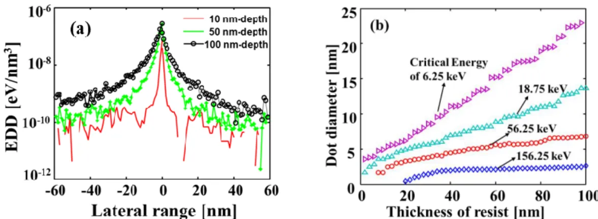
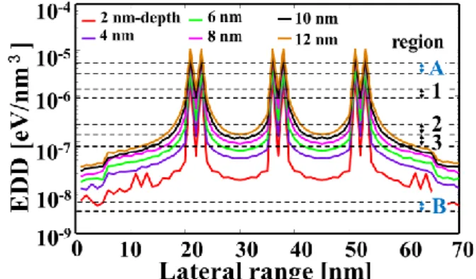
Process simulation is a key tool for optimization of the experiments. For example, most EB-exposures are performed with high-energy electrons (between 50 and 100 keV) because they provide very high resolution 17. Based on the analysis of trajectories of electron scattering, we can know that as the energy of incident electron increases, the range of trajectories become large 18. Furthermore, many researches have focused on the effect of resist thickness on pattern resolution 18-21. With calculating the energy deposition distribution in resist layer with various thicknesses, we can find that the standard deviation of EDD function in thin resist layer is smaller than in thick resist layer. A thinner resist film is advantageous to suppress the scattering of primary electrons in the resist film and to fabricate fine dot pattern. In addition, the simulation of research on the contrast of developer has been put forward for high resolution pattern fabrication with a dot size of <10 nm in these years 22-23.
1.2 The Purpose and Content of the Work
In this study, we try to use the simulation method to describe both the exposure process and development process. I tried to find the limitation factors of patterned resolution. I presented a general description of Monte Carlo simulation algorithm for modeling of exposure and development processes of EBL. In the exposure process, I established a home-made modeling of electron scattering with solid, and put forward a new modeling method of calculating energy deposition distribution (EDD) in resist layer. The EDD can instead of energy intensity distribution (EID) which can reflect on the energy deposition not only along the radius direction but also along depth direction. Based on it, I can calculate the energy deposition distribution for every depth of the resist. Furthermore, we calculated the trajectories of electrons at various incident beams and in different resists by using the home-made simulation. I demonstrated that thin resist, high incident beam, small electron beam size and negative resist can effectively make very fine dot arrays.
In the development calculation, Vutova and Koleva proposed a nonlinear model 23 using EID as a function of solubility rate to calculate the resist profile during development. However, the EID does not contain information about energy deposition distribution along the
depth-direction. The fundamental disadvantage of the nonlinear model is that the variation of the energy deposition along the depth direction is not considered in the simulation. Without the data of energy deposition in depth direction, it is difficult to reflect the change of solubility rates (development rate) with deposited energy variation in depth-direction. Even calculating the resist profile is impossible. However, the three-dimensional (3D) EDD can solve the problem of nonlinear model; it can reflect the energy deposition in depth-direction. Therefore, in this work, I proposed a new modeling for calculating the resist profile based on the 3D-EDD. The model, it is very important to determine the solubility rate based on the EDD for the development of latent patterns in the resist. By unifying solubility rate dependence of the exposure dose D (via experiment) and that of the EDD distributions (via calculations), I roughly calculated the solubility rates for 3D-EDDs by assuming that the EDD value is proportional to the exposure dose D. The development simulation was achieved by sequential calculation with solubility rates based on EDD, which was calculated by electron-atom scattering in Monte Carlo simulation. By determining a suitable EDD region (it is the same as selecting a suitable exposure dose in experiment) to make well patterning, I obtained a sharpened nano-dot pattern of resist. I demonstrated the results of the new model agree well with the experimental results. Moreover, based on the model, I changed the exposure conditions such as Gaussian beam size, incident energy and the development conditions such as using developers with various concentrations of NaCl to analyze the dependence. In addition, in order to study the effect of exposure dosage interval on the contrast of resist and the resolution of pattern, I tried to calculate HSQ resist developed profiles with various intervals of exposure dosage (∆𝐸𝐷𝐷). I demonstrated that the small dosage interval between the exposure dosages which correspond to maximum and minimum solubility rates is an important parameter for increasing the resolution of pattern. If a resist can form very fine pattern during a large range of exposure dosages, it can be demonstrated that the resist have good performance of exposure allowance. I selected two kinds of developers with high contrast and low contrast, respectively. Then I tried to observe that very fine dot arrays can be formed in which EDD region by selecting a series of EDD regions with ∆𝐸𝐷𝐷 of each developer. And I demonstrated that high contrast resist has the large exposure allowance and it is very useful for fabricating nano-sized dot arrays. I expect this study can
give us a deep understanding of improving the resolution of EBL by increasing the contrast of resist.
In summary, this thesis provides advances in EBL-based technological processes. In the exposure process, the electron-atom interaction in multi-layered solid thin film of resist by using Monte Carlo technique has been studied. Furthermore, a new method of calcualting the energy deposition distribution in the resist layer has been proposed, it is different as the energy intensity distribution. In addition, optimization of EBL has been accomplished by using proximity effect correction methods. In the development process, a new modeling method for calculationg developed profiles with a solubility rate based on EDD has been put forward. And the development behavior is studied for the different developers with various solubility rates. Moreover, the fundamental of increasing the contrast of resist has been discussed by change the interval of exposure dosage. The high contrast resist with the good performance in exposure allowance has also been demonstrated. Based on the analysis of simulation and experiment, I explore the possibility of resolution improvements in EBL.
1.3 The Outline of the Research
I divided the thesis into 7 parts as follows:
1. Chapter 1 briefly reports the nano-scale related aspects, needs for patterned media, fabrication methods for patterned media, the background of the research and the content of the work. This section aims to frame the contents of this thesis, coherently. It is intended to address the specific subjects under discussion or contained in the following chapters.
2. Chapter 2 briefly reviews the current development of electron beam lithography in nanofabrication, the fundamental of EBL, the electron-solid scattering process, different kinds of resists and the development process. From this section, we obtained a roughly understanding of the limiting factors of resolution in EBL such as resist material, the contrast of developer and so on.
3. Chapter 3 introduces the fundamental of the electron scattering process. In this study, I made home-made energy deposition distribution modeling and applied it to investigate under various conditions of electron traversing inside multi-layered thin
film of resist on Si. Using this simulation, the effects of incident energy, resist thickness and critical energy for development on nanometer sized pattern formation have been studied. The aim of the section is to investigate EB lithography using electron energy deposition distribution to ensure the higher resolution.
4. In Chapter 4, Gaussian beam instead of point beam shows in Chapter has been used to calculate the energy deposition distribution. The factors that determine the quantitative characteristics of the spatial distributions, such as beam voltage, beam sharp, beam size, beam distribution, resist material and film thickness etc. have been discussed.
5. In Chapter 5, a new development model of calculating the resist profile based on
EDD with solubility rates has been proposed. The relationship between EDD and
exposure dosage D has been estimated. And the EDD value is proportional to the exposure dosage D has been demonstrated. Using the relationship between D and
EDD, I selected various EDD regions to evaluate the quality of resist profiles. And
then, a suitable EDD region which can form a sharpened nano-dot pattern has been determined. The simulation results agree well with the experimental results by using high contrast developer with a combination of 2.3 wt% TMAH and 4 wt% NaCl developer. The effective of the new modeling for calculating resist profile has been demonstrated.
6. In Chapter 6, I investigated the factors that effect on the contrast of HSQ resist by using our proposed modeling method. I tried to calculate HSQ development profiles with different intervals of exposure dosage (∆𝐸𝐷𝐷). I demonstrated the ∆𝐸𝐷𝐷 is an indicator of contrast of resist and pattern resolution. In addition, I also demonstrated that high contrast developer as TMAH 2.3 wt% and NaCl 4 wt% developer has the small exposure interval, and the high contrast developer can provide high resolution patterning. Furthermore, I demonstrated that the high contrast developer has the good exposure allowance.
References
1. Z. Mohamad, M. Shirai, H. Sone, S. Hosaka and M. Kodera, Nanotechnology 19 025301 (2008).
2. A. Kikitsu, J. Mag. Mag. Mater., 321 526 (2009). 3. R. Wood, J. Mag. Mag. Mater., 321 555 (2009).
4. https://www1.hgst.com/hdd/research/storage/pm/index.html 5. W. Chang and J. R. Cruz, IEEE Trans. Magn. 46:11 3899 (2010).
6. S. J. Greaves, H. Muraoka, and Y. Kanai, J. Magn. Magn. Mater., 324 314 (2012).
7. F. Akagi, M. Mukoh, M. Mochizuki, J. Ushiyama, T. Matsumoto, and H. Miyamoto, J. Magn. Magn. Mater., 324 309 (2012).
8. S. Ma, C. Con, M. Yavuz and B. Cui, Nanoscale Research Letters 6 446 (2011).
9. H. Duan, D. Winston, J. K. W. Yang, B. M. Cord, V. R. Manfrinato, and K. K. Berggren, J. Vac. Sci. Technol. B 28(6) C6C58 (2010).
10. S. Hosaka, H. Sano, K. Itoh, H. Sone, Microelectron Eng. 83 792 (2006).
11. Z. Mohamad, M. Shirai, H. Sone, S. Hosaka, M. Kodera, Nanotechnology 19 025301 (2008).
12. W. J. Word, I. Adesida, P. R. Berger, J. Vac. Sci. Technol. B 21(6) 12 (2003). 13. S. Choi, M. J. Yan, L. Wang, I. Adesida, Microelectron Eng. 86 12 (2003).
14. B. Cord, J. Yang, H. Duan, D. Joy, J. Klingfus, K. K. Berggren, J. Vac. Sci. Technol. B 27(6) 2616 (2009).
15. X. M. Yang, S. Xiao, W. Wu, Y. Xu, K. Mountfield, R. Rottmayer, K. Lee, D. Kuo, and D. Weller, J. Vac. Sci. Technol. B 25 2202 (2007).
16. J. K. W. Yang, B. Cord, H. G. Duan, K. K. Berggren, J. Klingfus, S. W. Nam, K. B. Kim, and M. J. Rooks, J. Vac. Sci. Technol. B 27 2622 (2009).
17. K. Mitsuishi, Z. Q. Liu, M. Shimojo, M. Han, and K. Furuya, Ultramicroscopy 103 17 (2005).
18. H. Zhang, T. Tamura, Y. Yin, and S. Hosaka, Key Eng. Mater. 497, 127 (2012).
19. J. Fujita, Y. Ohnishi, S. Manako, Y. Ochiai, E. Nomura and S. Matsui, Microelectronic Eng. 42 323 (1998).
20. V. Sidorkin, A. Grigorescu, H. Salemink, and E.V. D.Drift, Microelectronic Eng. 86 749 (2009).
21. S. Hosaka, Y. Tanaka, M.Shirai, Z.Mohamad, and Y. Yin, Jpn. J. Appl. Phys., 49, 046503 1-3 (2010).
22. J. K. W. Yang and K. K. Berggren, J. Vac. Sci. Technol. B 25(6) 2025 (2007).
23. K. Vutova, E. Koleva, G. Mladenov, I. Kostic, T. Tanaka, Microelectronic Eng. 87 1108 (2010).
Chapter 2 Electron Beam Lithography
2.1 Nanolithography
The main goal of lithography is to create a desired pattern in a resist layer and to subsequently transfer pattern into or onto the underlying layer or substrate 1. The basic steps of a lithographic process are schematically illustrated in Fig.2.1.
First, the substrate (often silicon) is cleaned using chemical treatments or plasma procedures in order to remove contaminants which may lead to poor adhesion or defect formation in the resist layer. In the next step, a resist layer is spin-coated onto the substrate. Thinner resist layers can be obtained by using solutions with a higher dilution rate. After this, the sample is baked on a hotplate in order to remove the excess solvent from the resist and to thermally anneal residual stress in the resist layer. Next, the sample is e-beam-irradiated causing chemical changes in the exposed area during EBL. Following e-beam exposure, the sample is baked again to either thermally anneal the sample, in order to reduce unwanted chemical changes that might have been caused within the resist layer during the exposure, or to promote further chemical changes in the exposed or unexposed area. This step is referred as a post-exposure-bake (PEB). Subsequently, the sample is developed through spray, puddle or immersion method. A resist can have a negative or positive tone depending on whether the unexposed or the exposed regions are removed during the development process. Usually, the developed patterns are transferred into or onto the underlying layer or substrate by using techniques such as etching or lift-off. Finally, the resist structures are removed by a liquid stripping process or dry oxygen plasma etch. Lithography machines and resists play a crucial role in advanced nanolithography.
2.2 Electron Beam Lithography
EBL has been used in the IC industry since the 1960s. However, because of its very low throughput, its application is limited to small volume production such as fabrication of photo masks to be used for photolithography and in device prototyping 2. The first EBL tool was built based on scanning electron microscope (SEM) 3-4. In EBL tool, the electron beam is accelerated and focused onto a sample under a vacuum environment. While an SEM raster the beam on a sample to image the sample surface, an EBL tool finely focuses electron beam to any position of a sample for a particular duration and draws a shape by controlling the position, and blanking of the
beam. Patterning requires a deflection and blanking systems which uses electrostatic or electromagnetic lenses to control the beam position, as shown schematically in Fig. 2.2. As an EBL tool can draw an arbitrary pattern, it is categorized as a mask less lithography.
EBL provides excellent resolution due to a small probe size 5-7. In addition, EBL is a flexible patterning technique that can work with a variety of materials. There are two main EBL strategies, projection printing and EB drawing. In projection printing, a large EB mask pattern is projected onto a resist layer through the mask by using a high-precision lens system. In EB drawing, a small EB spot is moved on to the sample to draw figure with one by one pixel. Direct EB drawing can eliminate the expensive and time-consuming production of masks because the drawing can directly fabricate the resist pattern on the sample. Typically the drawing field, which is deflection range of the beam on the sample, is 10 micrometers to a few millimeters. Larger patterns require mechanical stage movements, which need to be very accurate in order to precisely stitch many drawing fields. The backscattered electrons from the substrate cause to expand the energy deposited areas, which is called by proximity effect. In
order to draw the pattern precisely, we correct the drawing pattern to eliminate the proximity effect. However, the proximity effect causes to deteriorate the patterning resolution. This cannot be corrected in practical EB drawing. In order to reduce the proximity effect, multi-resist method has been developed. Based on the discussion as above, in the next sections, we will use simulation to analyze the patterning resolution in EB drawing and to improve the pattern resolution for highly packed dot arrays.
2.3 Electron-Solid Interactions
Although the electron beam in EBL tools can be tightly focused to an extremely small beam diameter of less than few nanometers, it is also difficult to achieve a nanometer sized feature in a resist film. Electron–solid interactions 8 cause electron scattering in the resist film. When electrons inject into the resist, the energy deposits in the resist film due to electron scattering and inelastic energy loss. The energy deposition distribution provides a limitation of EB-drawing patterning. As primary electrons strike the resist, they experience two types of scattering events, forward scattering and backscattering, as shown in Fig.2.3. The forward scattering 9-10 causes incident electrons to change their direction by a small scattering angle, and to broaden the beam penetration area as electrons penetrate toward the bottom of the resist film. The backscattering occurs due to a large angle scattering event. It usually happens when primary electrons collide with an atom. Some backscattered electrons travel back to the sample surface through the resist at a range as far as micrometers away from the incident beam. These backscattered
electrons cause the proximity effect. It causes that the feature connects with neighbor feature when they are located in a distance of less than 100 nm, or the feature size increases from the designed size (see Fig.2.3).
Primary electrons can experience inelastic scattering events in the resist film and dissipate their energy to form pattern (see Fig. 2.4). The energy dissipation continues and
Fig.2.3 Representation of electron dose absorbed in the case of isolated (left) or areal (right) features.
generates energy deposition along the scattering pathway of the primary electron until the primary electron loses all of its energy, initially between 5 and 50 keV in EBL. Secondary electrons with energies in a range of 2 to 50 eV are generated for the majority of resist exposure process. They are considered to cause additional beam diameter widening as they can travel a short distance, less than nanometers in the resist. This effect can be neglected because of extremely small range.
Fig.2.4 Schematic diagram of electron-solid interactions in resist and substrate. The electron-solid interactions may cause that absorbed energy distribution confined to the zone where the electron has been traveled. The effective exposure in a point is influenced by others exposed at neighbor points based on reciprocity principle. The choice of system configuration or exposure conditions can minimize it, for example, the use of very thin resist layer or beam energy selection and also the design program can allow correcting the proximity effect.
2.4 Electron Beam Resist
Electron beam resists are sensitive to the energy of the electron beam. The chemistry of the resist defines the relationship of the absorbed energy to the change of the molecular weight of the resists. The resist solubility depends on the molecular weight or size in developer 11. Typically in electron beam lithography, the energy of the primary electrons is 10–100 keV, but lower and higher energies also have been used. Since EBL is used for many different purposes, many properties of the resists have been developed. Usually, high resolution and high sensitivity are the most required properties of the resist. But when we want to transfer the resist pattern to the substrate, etching resistance of the material might be
more important together with above property.
The continuous researches on new resist materials and development chemistries have led to a wide variety of commercially available resists and developers. Resists are dissolved in a liquid solvent and they are spread on a substrate by spin coating in most cases. This is the most reproducible method. Other coating techniques such as spray, roll and dip coating are also used, but they produce less uniform layers. After spreading the resist the solvent is removed by soft bake (also called prebake). Soft bake affects the outcome of the exposure and development and therefore the baking should be done carefully, keeping the conditions and procedure constant. After electron beam exposure, the pattern in the resist is brought out in development. The resist is developed by immersion, spray or puddle method. Immersion development can be done simply in any chemical resistant vessel, but spray and puddle development methods require dedicated equipment. Since the latter two are automated processes, their reproducibility is better.
Resists are divided to two groups by their response to the energy of the electrons: those which are more soluble to the developer liquid after the irradiation are called positive and those which get less soluble are called negative. In general positive resists are used for making concave profiles and negative resists for making convex profiles. In this section, we introduce some positive resists and negative resists.
2.4.1 Positive resist
Poly(methyl methacrylate) (PMMA) is one of the early stage resists developed for EBL12. PMMA is typically used as a positive tone resist (Fig. 2.5), although it acts as a negative tone resist at very high dose, about two orders of magnitude greater than that used for the positive tone behavior. Upon EB irradiation, the polymer can undergo either bond breaking (chain scission) or radiation-induced bonding (crosslinking) simultaneously. Chain scission dominates in the positive tone mode of PMMA, leading to reduction of the molecular weight of the polymer, and thus enhancing solubility in particular developers. Crosslinking events forming a heavy molecular weight polymer, which becomes insoluble, dominate in the negative tone mode of PMMA.
Fig. 2.5 Chemical structure of PMMA ((C5O2H8)n).
PMMA has a capability for high resolution, and its ultimate resolution has been demonstrated to be less than 10 nm 13. The major problems of PMMA are its relatively poor sensitivity, poor dry etching resistance, and moderate thermal stability. Other important positive resists include PBS (PolyButene-1-Sulfone) and EBR-9 (a copolymer of trifluoroethyl a-chloroacrylate and tetrafluropropyl a-chloroacrylate) which have high sensitivity and ZEP (a copolymer of chloromethacrylate and methylstyrene) which has high-resolution. It is noted that the desired properties of a resist are high-resolution and high sensitivity (high speed). Unfortunately, the resist that have higher sensitivity, usually have lower resolution, especially compared to PMMA.
2.4.2 Negative resist
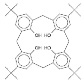
Negative resists tend to have less bias but they have problems with scum and swelling during development and bridging between features. Calixarene as one of popular negative resist is a cyclic oligomer containing repeating units of phenolic hydroxyl groups linked with methylene bridges (Fig. 2.6). Various calix[n]arene derivatives have been studied as the negative tone resists for EB lithography 14. With molecular size of about 1 nm, the material has the potential for high resolution lithography. Sub-10 nm feature resolution was achieved in a film of p-methyl-acetoxycalix[6]arene.
Fig. 2.6 Chemical structure of calix[4]arene with para-tert-butyl substituents (C36H36O4Cl4).
In the last decade, HSQ (Flowable Oxide, Fox-12 from Dow Corning) has become a serious candidate for a high-resolution e-beam resist because of its small line edge roughness,
high etching resistance and small molecular size 15 (Fig. 2.7). HSQ is also an excellent resist for testing EB machine resolution limits because HSQ lines on silicon can be imaged directly in a SEM without the need for gold evaporation for conduction or “lift-off” techniques 16. Sub-10-nm isolated and dense features have been successfully fabricated using 100 keV EBL 17
. The properties of the resist (e.g. contrast, sensitivity, etching resistance) are influenced by numerous factors ranging from the manner of storage to the details of the development process.
Fig. 2.7 Chemical structure of HSQ (H8Si8O12).
2.5 Development Process
Besides the lithography tools and resist materials, the development process plays an important role in the EB patterning. Usually, HSQ is developed by manual immersion in aqueous solutions of different developers, tetramethylammonium hydroxide (TMAH) being one most frequently used 18. Namatsu suggested that the development of HSQ in alkaline solutions is related to bond scission by ionization and that the dissolution rate strongly depends on the bond strength 15. At low exposure doses, the dangling Si bonds are not stable and the unexposed and slight exposed areas close to the pattern are easily dissolved even when using a weak developer. At a high exposure dose, the Si bonds become more stable due to network formation and the dissolution rate of HSQ decreases remarkably. In this case, a strong developer is recommended because it might improve the dissolution rate due to its effectiveness in bond scission. That means that the optimum dose shifts to higher doses, improving the contrast but decreasing the sensitivity. The main risk of using a strong developer for nanostructures is that structures may be washed away and only highly exposed areas remain on the substrate 1. While a low developer concentration is used, the sensitivity increases but the contrast is reduced because part of the slightly exposed area near the pattern remains on the substrate. In order to form pattern with fine resolution, the research on finding
suitable concentration of developer is very necessary to be done.
2.6 Conclusions
In this section, we briefly introduced electron beam lithography, several kinds of resists and the importance of the development process. I had obtained an understanding of that the performance of both the lithographic tool and the resist material can limit the resolution of resist-based EB lithography. In order to successfully form very fine nano dot arrays, I should study the various factors that limit the resolution, such as resist material, writing strategy, beam size, resist thickness and development process. In the next chapters, I will investigate these factors in exposure and development process to find the resolution limitation, and then to improve the resolution of patterns.
References
1. A. E. Grigorescu and C. W. Hagen, Nanotechnology, 20 292001 (2009).
2. McCord, M. A., Rooks, M. J., Handbook of microlithography, micromachining, and microfabricaiton, Vol. 1, 144 (1997).
3. K. Mitsuishi, Z. Q. Liu, M. Shimojo, M. Han, and K. Furuya, Ultramicroscopy, 103 17 (2005).
4. L. Li, S. B. Long, C. S. Wang, W. G. Wu, Y. L. Hao, M. Liu, Microelectronics Journal, 37 317 (2006).
5. A. A. Tseng, K. Chen, C. D. Chen, and K. J. Ma, IEEE TRANSACTIONS ON ELECTRONICS PACKAGING MANUFACTURING, 26 141 (2006).
6. S. Hosaka, H. Sano, M. Shirai, Y. Yin and H. Sone, Microelectronic Eng., 84 802 (2007). 7. S. Manako, J. Fujita, Y. Ochiai, E. Nomura and S. Matsui, Jpn. J. Appl. Phys., 36 7773
(1997).
8. H. S. Wong, N. R. Buenfeld, Cement and Concrete Research, 36 1076 (2006). 9. R. Shimizu, Z. J. Ding, Rep. Prog. Phys., 487 (1992).
10. M. S. Son, B. H. Lee, M. R. Kim, S. D. Kim and J. K. Rhee, J. Korean Phys. Soc., 44 408 (2004).
11. M. Kean, D. R., Schaedeli, U., M. Donald, S. A., J. Polym. Sci., Part A: Polym. Chem., 27, 3927-3935 (1989).
12. M. Cord, M. A., Rooks, M. J., Handbook of microlithography, micromachining, and microfabricaiton, 1, 205 (1997).
13. M. Khoury and D. K. Ferry, J. Vac. Sci. Technol. B, 14 75 (1996). 14. S. Yasin, D.G. Hasko, H. Ahmed, Appl. Phys. Lett., 78, 2760 (2001).
15. H. Namastu, Y. Takahashi, K. Yamaguchi, M. Nagase and K. Kurihara, J. Vac. Sci. Technol. B, 16 69 (1998).
16. J. P. Weterings, A. K. van Langen-Suurling and H. Romijn, J. Vac. Sci. Technol. B, 18 3419 (2000).
17. M. J. Word, I. Adesida and P. R. Berger, J. Vac. Sci. Technol. B, 21 L12 (2003). 18. A. E. Grigorescu, C. W. Hagen and P. Kruit, Microelectron. Eng., 84 822 (2007).
Chapter 3 Monte Carlo Simulations of Electron Scattering
in Solid for Electron Beam Lithography
The formation of high-density, nanometer-scale dot (nanodot) arrays is a challenging task. Such arrays are considered important not only for scientific study of the fundamental quantum-mechanical behavior of materials, but also for achieving a practical goal of ultrahigh-density data storage and electronic devices. In particular, methods for producing isolated high density magnetic nanodot arrays with a pitch of 20 nm or less have been extensively studied with the aim of fabricating the next generation of patterned magnetic media with a recording density of up to 1 terabit inch-2. 1
EBL with extremely high-resolution is as one of the most promising methods for fabricating the nano-scale structures 2. However, charging-up and proximity effect can lead to poor pattern fabrication, especially it is very severe for high-density nanoscale features. Therefore, the understanding of electron beam interactions with samples and the physicochemical changes associated with these interactions are of vital importance to optimize the lithographic process for nanometer size-pattern. Based on the analysis of electron-atom interactions, correcting selection of the exposure and development conditions can ensure higher resolution and the desired resist profile and dimensions.
Monte Carlo EBL simulation technique has been already applied to single and multilayered samples of sub micron size to study electron beam interaction with atom 3-6. In the calculation of the deposited energy in the resist layer, the EID function7 was used. The EID function usually consists of two Gaussian functions with maximal values and dispersions. However, the EID function can reflect the energy deposition distribution in radial direction, we cannot get distribution of energy deposition in depth direction. In this study, we make our home-made EDD calculation program and apply it to investigate various conditions of electron traveling inside multi-layered thin film of resist on Si. Using this simulation, the effects of incident energy, resist thickness and critical energy for development on nanometer sized pattern formation have been studied. Our aim is to investigate EB lithography using electron energy deposition distribution to ensure the higher resolution and we also want to use
the results of the simulation to improve the results in experiments.
3.1 Elastic Scattering
3.1.1 Basics
Elastic scattering results from the interaction between incident electrons and the electrostatic field of an atomic nucleus as screened i.e. reduced in range and magnitude, by the atomic electrons. Because the large mass of the nucleus compared to that of the electron the average energy lost by the incident electron in such an interaction is very small and usually neglected. Therefore the incident electron is considered to change its direction without losing energy. This interaction is dominant and mainly occurs in the spatial distribution around the electron incident direction in the solid.
In general, we can write the differential cross section for elastic scattering / , which represents the probability of an incident electron being scattering per unit solid angle by the atom, as a function of complex scattering amplitude or scattering factor f, i.e.:
| (𝜃)| (3.1) where f is a function of the scattering angle 𝜃.
Within the first Born approximation f is proportional to the Fourier transform of the atomic potential 𝑉( ) with r the distance from the nucleus. By choosing a suitable expression for 𝑉( ) we can obtain an expression for the differential cross section for elastic scattering.
3.1.2 Rutherford cross section
The earliest and simplest model for elastic scattering of charged particles is based on the unscreened electrostatic field of a nucleus and was first used by Rutherford to study the scattering of alpha particles. A simple way to account for screening is given by using a so-called Wentzel potential in which the nuclear potential is attenuated exponentially as a function of the distance r as follow:
0 0 (3.3) where Z the atomic number of the target atom, e is the electronic charge, r0 is the screening radius and a0 is Bohr‟s radius.
The exponentially decaying function is a rough approximation of the screening of the nucleus by its atomic number. Using such a potential leads to following expression for the differential elastic scattering cross section 8:
𝑒
𝐸 ( 𝑜 ) (3.4) with 𝛼 being the so-called screening factor and defined as:
𝛼 𝐸 𝑟 𝑚 𝑒 𝐸 (3.5) In the special case of no-screening (i.e. 𝛼 ) we obtain the well-known Rutherford formula:
𝑒
𝐸 ( 𝑜 ) (3.6) The total elastic Rutherford cross section 𝜎𝑒 is obtained by integrating Eq.3.6 over all possible scattering angles:
𝜎𝑒 ∫ . / 𝑑 ∫ n 𝜃0 . / 𝑑𝜃 (3.7)
3.1.3 Mott cross section
The screened Rutherford cross section is only valid for incident electrons with sufficiently high energy (a few keV) and for atoms with intermediate atomic number Z. For lower energies and heavy elements it does not correctly describe elastic scattering since in the derivation of the differential cross section we have ignored the spin of the incident particle and subsequent spin polarization effects. Also, the simplistic exponentially decaying atomic potential V(r) we have used should be replaced by a more realistic one. A differential cross section which incorporates all these factors in detail is the Mott cross section 9-12. According to Mott (Mott,1929), by solving Dirac equation a relativistic representation of the differential elastic scattering cross section is given by
| (𝜃)| | (𝜃)| (3.8) where the scattering amplitudes is derived by a partial wave expansion method 10-12 (Mott & Massey, 1965):
(𝜃) 𝑖𝑘∑ 0( ). 𝑖 / ( 𝑖 )1
𝑙 0 𝑃𝑙( 𝑠𝜃) (3.9)
(𝜃) 𝑖𝑘∑ 0 𝑖 𝑖 1
𝑙 𝑃𝑙 ( 𝑠𝜃) (3.10) where is the electron momentum, 𝑃𝑙( 𝑠𝜃) and 𝑃𝑙( 𝑠𝜃) are Legendre and the first order associated Legendre functions, 𝛿𝑙 and 𝛿𝑙 are the phase shifts of the l th partial wave for spin up and spin down electrons, respectively.
The total elastic cross section 𝜎𝑒 can be obtained by integrating the differential elastic scattering cross section over whole solid angles,
𝜎𝑒 ∫ 𝑑 ∫ 𝑠 𝜃*| (𝜃)|0 | (𝜃)| +𝑑𝜃 (3.11) which is related to elastic scattering mean free path in solid via
𝑒 ( 𝜎𝑒) (3.12) where 𝑁 𝜌/ is the number of atoms in a unit volume, NA is Avogadro‟s number, 𝜌 is the density and A is the atomic weight.
The elastic scattering mean free path is the average distance between two successive elastic collisions between a moving electron and solid atoms, which is the basic information requested in the MC simulation for electron transport in solids.
3.2 Inelastic Scattering
The inelastic electron-atom collisions result in electron energy loss due to such effects as generation of secondary electrons, bremsstrahlung emission, or Plasmon excitation. A single stopping power (i.e. energy loss per unit electron path length) is used to model electron energy loss due to all possible inelastic scattering events between two subsequent elastic scatterings. The commonly used electron stopping power is that defined by the Bethe law.
𝐸 𝑒 𝐸 𝐸 (3.13) where n is the number of atoms in a unit volume. J is an adjustable parameter called mean ionization potential and defined empirically as a function of the atomic number. Another issue of using Eq. (3.13) is that it gives a negative value on the right hand for electron energies smaller than J/1.166.
Bethe law 13-14 that should be more adequate for high (50-100 keV) energetic electrons. In compact form, the relativistic Bethe formula can be written as
𝐸 𝑒 𝑚 0 𝑚 𝐸 ( 𝛾 𝛾 ) 𝛾 ( 𝛾) 1 (3.14) where v is the relativistic electron velocity, which relates to the given kinetic energy 𝐸 (𝛾 ) via relativistic correction factor 𝛾 √ (𝑣 ⁄ ) . m is the electron rest mass. As for the value of J, it was calculated according to Berger and Seltzer similar to the case of the usual Bethe formula above.
One of the commonly used expressions for the stopping power is given by the modified Bethe relationship, which is expressed as 15
𝐸 𝑧 𝐸 . (𝐸 0 ) / (3.15)
Here J, the mean ionization potential, is assumed to be available from the experiments. The shortcomings of the Bethe relationship is that it incorrectly represents the stopping power at low electron energies (i.e., <1 keV). The experimental data demonstrated a wider range of application in various electron energies, and they can be easily incorporated in a Monte Carlo Method (MCM) which further improves the accuracy of MCM results.
3.3 Monte Carlo Modeling
Various models for Monte Carlo simulation, which have been widely used since the start of this approach in the 1960s, are briefly explained below.
3.3.1 Multiple scattering model
This model, initiated by Berger (1963)16 for practical Monte Carlo calculations of penetration of charged particles in matter, was based on the use of the Bethe‟s stopping power equation describing energy loss and angular distributions for electron scattering, which is derived for a certain electron path, s, from the transport equation
(𝜃) (4 ) ∑ ( )𝑃 𝑙
𝑡 0 ( 𝑠𝜃) ∫ 𝐾0 𝑙𝑑𝑠 (3.16) where
with 𝑃𝑙( 𝑠𝜃) is the Legendre polynomial, and 𝜎(𝜃) is the screened-type Rutherford scattering cross-section. For applications of this type of Monte Carlo calculation as applied to EPMA the reader may find the work by Heinrich (1968) 17 very useful and instructive. This model was superseded by the single scattering model.
3.3.2 Single Scattering Model
This model 18, which is still widely used, adopts the screened Rutherford scattering cross-section 𝜎𝑅(𝜃) in place of the angular distribution (𝜃) represented by Eq. (3.16) while the energy loss calculated by Bethe‟s stopping power equation as in the multiple scattering model. Wider applications of this model will be mentioned in section 3.4.
3.3.3 Hybrid model
In this model each individual inner-shell ionization was simulated according to Gryzinski‟s formula 19. The energy loss due to valence electron excitations was imposed on each step length between two individual scattering events in the so-called continuous slowing down approximation, being assessed directly by
∆𝐸 ∫ . 𝐸 / 𝑎𝑙𝑒𝑛 𝑒
0 𝑑𝑠 (3.18) where the stopping power of valence electrons was estimated by the difference of Bethe‟s stopping power and the stopping power of the inner-shell electrons, ∑ ( 𝑑𝐸 ⁄ 𝑑𝑠)𝑛 𝑛,
. 𝐸 / 𝑎𝑙𝑒𝑛 𝑒 . 𝐸 /𝐵𝑒𝑡 𝑒 ∑ . 𝐸 /𝑛 𝑛 (3.19) where, according to Gryzinski,
( 𝑑𝐸 𝑑𝑠)𝑛 𝑁 ∫ (∆𝐸) 𝐸 𝐸𝑛 𝑑𝜎𝑛 𝑑(∆𝐸)𝑑(∆𝐸) π 𝑁𝑧𝑛 𝐸( 𝐸 𝐸𝑛 𝐸 𝐸𝑛) 3 × [ .𝐸𝐸 𝑛/ 3 ( √ 𝐸 𝐸𝑛 )] (3.20)
This hybrid model, initially proposed by Schneider and Cormack (1959) for the discrete and continuous energy loss processes, has been further developed by some authors (e.g. Berger 1963, Shimizu et a1 1972, Reimer and Krefting 1976, Shimizu 1977, Shimizu and
Everhart 1978, Ich'mura and Shimizu 1981, Murata et af 1981, Reimer and Stelter 1986), and has done much to extend Monte Carlo calculations to alloys and compound materials including secondary electron generation.
3.4 Modeling of Electron Scattering Process
When a beam of high energy electrons hits a solid target, the electrons will interact with the electrical fields of the target‟s atoms and undergo elastic and inelastic scattering events. In elastic scattering, the incident electron is deflected with no energy loss. In this study, for the treatment of electron elastic scattering, we considered the incident electron energy of 10 keV-30 keV, while the Mott scattering model was just used for the low energy. Here, we selected the screened Rutherford scattering model 20-21 as the elastic model:
𝑖
𝑒 𝑖( 𝑖 )
𝐸 ( 𝑜 𝛽) (3.21) where 𝛽 is the screening parameter which is given by
𝛽 . 𝜆 𝑝 / (3.22)
0 / 0 (3.23) where e is the electronic charge, Z is the atomic number of the material, E is the energy of electrons, θ is the scattering angle, a0 is the Bohr radius, h is the Planck's constant and p is the electron momentum.
The scattering step length of electron with energy E is derived from the following formula:
𝑆 𝑁 ∙ ln (3.24)
where σ is the total cross section calculated from differential scattering cross section, N is the Avogadro's number, A is the atomic weight and is the mass density, R is a uniform random number between 0 and 1.
Scattering angle 𝜃 and azimuthal angle 𝜙 can be obtained using the following equations:
θ 𝑠 . 𝛽𝑅
𝜙 π (3.26)
where the R1 and the R2 are independent equidistributed random number between 0 and 1. Since the electron suffers scattering to make its trajectory, it continuously loses its kinetic energy to make its trajectory. Figure 3.1 shows the flow chart of the Monte Carlo simulation program. In the simulation, incident electron is slowing down following Bethe's formula, which is a good empirical method of calculating this energy loss in electron-atom interaction. The Bethe's approximation 20 is given by 𝐸 𝑒 𝐸 ∑ 𝑖 𝑖 𝑖ln . 𝐸 𝑖 / (3.27)
where the 𝑖 is the number of atoms in a unit volume, the 𝐽𝑖 is mean ionization energy of atom i .
The energy just before the nth scattering is:
𝐸𝑛 𝐸𝑛 |𝑑𝐸/𝑑𝑠|𝐸𝑛 ∙ 𝑆𝑛 (3.28)
where the 𝐸𝑛 is the energy of the (n-1)th scattering, the 𝑆𝑛 is step length between (n-1)th and
nth scatterings, and the |𝑑𝐸/𝑑𝑠|𝐸𝑛is the mean energy loss rate which can be obtained from Eq.(3.27).
3.4.1 Determination of scattering center in polybasic material
When we select the polybasic material as the resist, for each scattering of electron in simulation, it must be determined by random sampling which element atom will act as the scattering center, then the scattering step length, scattering angle and energy loss are calculated.START Choose Scattering Center
Calculation 1 : Total Cross Section
Boundary Treatment Next
Scattering
END
Coordinate Transformation Calculation 2 :Step Length
and Scattering Angles
Y
Z<0
N
Calculation 3 :Energy Loss E (i+1)=E (i) -ΔE
E >50eV
N
Y
Y
Cross the Border ?
Fig.3.1 Flow chart of the home-made Monte Carlo simulation program.
Based on the Rutherford-Bethe model, the formula ∑𝑘 𝑖 0𝑃𝑖 < ≤ ∑𝑘𝑖 0𝑃𝑖 ( … 𝑁) is used to determine whether the k-th element atom acts as the scattering center in the medium with N kinds of elements, here 𝑃𝑖 denotes the probability of scattering off an atom of the i-th element and R is a uniform random number distributed between 0 and 1.
3.4.2 Multilayer system
For a multilayer system, i.e. a sandwich-like sample, special attention should be paid to the existence of an interface between two layers, in regard to the various possibilities of the location of path over different layers that possess unequal mean free paths for electron travel.
When there is a large difference in atomic number between a film and a substrate, boundary treatment is significant for electrons crossing the interface as shown in Fig. 3.2.
Fig.3.2 Sketch of the electron path crossing the boundary.
The boundary treatment equation is
𝑆 𝑂̅̅̅̅ 𝑂𝐵̅̅̅̅ ∙ / =0 (3.29) where S is step length starting at Point A before correction, and are respectively the mean free paths in the two kinds of mediums Ⅰand Ⅱ of electrons with energy 𝐸 . If S > 𝑂̅̅̅̅, the corrected 𝑂𝐵̅̅̅̅ should be calculated, it can be obtained from Eq (3.29) is the scattering length of electron in medium Ⅱ. Thus, the real step length after correction of the