Effectiveness of Instruction using Electronic Circuit
Simulation Software
Yukio OHTA and Atsuo MURATA
Department of Intelligent Mechanical Systems, Division of Industrial Innovation Sciences
Graduate School of Natural Science and Technology, Okayama University
3 – 1 – 1, Tsushimanaka, Okayama – Shi, 700 – 0085, Japan
[email protected]Abstract— Traditional teaching (lecturing) method on the design of electronic circuit provides learners with little satisfaction, because they cannot check and confirm the validity of electronic circuit they have designed. A better way to acquire design skills is to actually make the designed electronic circuit and test the validity of design. In spite of the usefulness of such a practical approach, it has a disadvantage that there is only limited time for teaching (lecturing) and it is difficult to fabricate electronic circuit, perform electronic measurement, and test the validity of design in the limited lecture period. An alternative to overcome these disadvantages is to use simulation software that enables learners (students) to operate functionally the designed electronic circuit and verify the appropriateness of design. The aim of this study was to examine the usefulness of simulation approach and clarify some problems related to such an approach.
I. INTRODUCTION
When teaching how to design electronic circuit, the following steps are, in general, necessary: (1) understanding the physical characteristics of semiconductor, (2) understanding of functional elements of semiconductor, and (3) learning of electronic circuit ([1] Tietze and Ch.Schenk (1991)). However, such an approach requires many hours to understand the electronic circuit and acquire how to design electronic circuits. Moreover, using such a method without practical learning process, it is more and more difficult to understand electronic circuit during a short learning period. Even if the electronic circuit was successfully designed with proper teaching method, it is difficult to test the validity of designed circuit. A direct method to overcome such a defect is to assemble a designed circuit and measure its physical characteristics, which requires not only the ability to design electronic circuit but also the ability to assemble the circuit and measure the physical characteristics. As such a procedure is time consuming, it is impossible to practice such a procedure.
As an effective approach to overcome the problems above mentioned, the utilization of electronic circuit simulation software to enhance the teaching efficiency is demonstrated, and the effectiveness of such an approach is discussed.
In a lecture, using such a simulation software, students were firstly provided with the design method of electronic circuits. Secondly, the designed circuit was entered into a
simulator to carry out a simulation and display the result. If the design was adequate, the desirable characteristics are displayed. For the inadequate design, an error message is displayed. This enabled students to know the adequacy of the designed circuit for a short period.
When the designed circuit is inadequate, the confirmation and verification of designed circuit, the alteration of parameters for the design of circuit, and the re-execution of simulation are carried out. Such a procedure leads to easy detection and modification of error. This approach also has an advantage that elements of circuit are not damaged.
In this study, effectiveness of Instruction using Electronic Circuit Simulation Software was demonstrated and discussed. Some problems related to such an approach was also identified to further improve the teaching efficiency.
II. ELECTRONIC CIRCUIT SIMULATION SOFTWARE
Electronic Circuit Simulation Software, PSpice (US Cadence Design Systems, Inc.) ([2] J.A.Svoboda, [3] P.Tobin), was used in this study. The software belongs to OrCAD PSpice product family, which includes the following products.
A. OrCAD PSpice A/D
This system is a higher version of PSpice, and a Analog/Digital mixed simulator. This system can simulate Analog/Digital mixed circuit ranging from IGBT or PWM to DAC or ADC.
B. OrCAD PSpice
This is a simulator which includes all functions necessary for simulating analogue circuits. Using built-in models, this system can design from a system with a high frequency component to low-powered IC.
The circuit can be designed by selecting a proper device from the library. A new device model can be generated using a data sheet.
C. OrCAD PSpice A/D Basics Plus
This system is a preliminary Analog/Digital mixed simulator, and is proper for users who would like to carry out a simulation where analog and digital circuits are mixed up. This system is equipped with a basic analytic function of
Fourth International Workshop on Computational Intelligence & Applications
PSpice.
D. PSpice optimizer
This application system is used together with PSpice or PSpice A/D. This system can automatically conduct a repeated processing to enhance the accuracy of electric circuit design.
E. Figures and Tables
Place illustrations (figures and tables) throughout the paper at the places where they are first discussed in the text, rather than at the end of the paper. Number illustrations sequentially (but number tables separately). All illustrations must be centered. The number and caption of a figure must always appear below the figure. The number and title of a table always appear above the table.
The operating environment of this software was as follows:
CPU: Intel Pentium (DOS/V machine) OS: Windows NT 4.0, Windows 95, 98
Memory: RAM of more than or equal to 32MB (64MB is recommended)
Resolution of display: Minimum 800 X 600 pixel (1024 X 768 pixel is recommended)
III. SIMULATION USING PSPICE
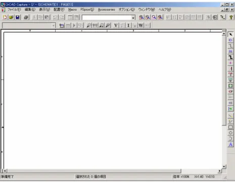
The design of a low-frequency amplifier is demonstrated. The design method of such a circuit is not described in detail. First, Schematics editor (See Figure 1 and 2) is booted to draw a circuit on the display.
A. Draw of electric circuit
By clicking [Parts call] menu in Figure 1, transistors, resistance, condenser, source of signal, and (or) power supply are arranged on the draw area in Figure 1. Next, [Wiring] menu enables us to connect each part. An example of drawing is shown in Figure 3.
B. Alternation of value of electronic parts
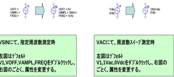
At the stage of drawing electronic circuit, the default values of each part are displayed. Therefore, these values must be altered by clicking the [Parts] menu. Then, according to the display for altering the values of each part, the alteration is carried out. In Figure 4, the wave of source of signal eg, its output voltage, frequency are set to sine wave, 100mV, and 1kHz, respectively.
C. Conditions for simulation
Once the drawing of electronic circuit was completed, conditions for the simulation must be set. The menu display for setting the simulation condition is shown in Figure 5. What kind of analysis is needed must be indicated to the software. Such an example (measurement of frequency characteristics of circuit) is illustrated in Figure 6.
To measure frequency characteristics, the [AC sweep] menu must be firstly selected. Next, the display to set a sweep
range is displayed as in Figure 7. Here, the sweep frequency of input signal ranged from 1Hz to 100kHz. Returning to the [analysis setting] menu in Figure 6, the [transient] menu is selected to show the display in Figure 8. Using the display, the analytical time of circuit is determined.
D. Determination of measurement sites
The markers to measure the waveform of signal must be arranged. The menu for the arrangement of markers is depicted in Figure 9. As selection of [Voltage difference] attaches symbol of voltage marker to the tip of cursor, bringing this to the part that should be measured completes to the preparation for voltage measurement.
E. Simulation execution
By clicking the [simulation start] button in Figure 2, the simulation starts and the display which shows that it is under analysis is presented to the user as shown in Figure 10. If there exist some errors in condition settings, the error message is displayed with red character. If no error was detected, the display to select the type of analysis is presented to the user (See Figure 11). After this procedure is completed, the results of analysis as shown in Figures 12 and 13 are output.
IV. RESULTS OF SIMULATION
When the expected results were not obtained by the simulation, the reason cannot be identified using a simulation system. In such a case, the designer must review the design process, identify the error and the reason, and modify the error. When the design does not have a fatal error (for example, the condition or value of each part is not correctly entered), the simulation was carried out again by entering proper parameters, and the correct result can be obtained. Although this approach is practically useful, we cannot recommend such an approach from the viewpoint of learning how to design electronic circuits.
Observing the simulation results in Figures 12 and 13, it is clear from Figure 12 that the gain at the low-frequency band is out of the designed (ideal) value. The cause of such outlier can be inferred as follows: The circuit in Figure 3 includes a negative feedback circuit in which the value of C6 and the reactance corresponded to C6=4.7μF and Xc=1/(ωC). The value of XC at the low-frequency band became larger due to the disfunction of negative feedback circuit.
Based on the observation above, the value of C6 was altered to 22μF and the simulation was carried out again. The result is depicted in Figure 13, which shows that the designed circuit is proper.
As mentioned above, using a electronic circuit simulation tool (PSpice), the characteristics of the designed circuit can be obtained without building the designed electric circuit. Moreover, the simulation tool enables us to judge the adequacy of the design without building the circuit. Such characteristics of simulation tool must lead to higher satisfaction of learners. It is also possible to determine
optimal design conditions using the simulation software. V. DISCUSSION
The effectiveness of teaching approach based on the simulation software must be evaluated systematically. The following questionnaires on the evaluation of teaching method in general were carried out to verify the proposed teaching method of electronic circuit design:
(1)Was the lecture easy to understand?
(2)Were you interests towards the lecture deepened? (3)Could you feel a zest of lecturer?
(4)Was the lecture carried out by taking safety aspects into account?
(5)Was the lecture carried out according to the syllabus? (6)Was the explanation or instruction easy to understand? (7) Did you think that the text was useful?
(8)Was the writing on the blackboard or AV equipment useful to understand the lecture?
(9)Was the lecture carried out by confirming the response of students?
The students also evaluated themselves using the following questionnaire:
(10) Did you attend every lecture?
(11)Did you make any efforts to improve your knowledge and skill?
(12)Did you submit every report directed by the lecturer? (13)Were you satisfied with the lecture?
These questionnaires were rated using a five point scale. Point 5 means that the satisfaction for each questionnaire item is the highest. Furthermore, the following questionnaire item was added to the evaluation process.
(14)Which was better, the lecture on the first term or the lecture on the latter term?
The answer was: (A)first term, (B)latter term, and (C)both are equal.
The results of questionnaire survey are summarized in Table 1. The results clearly show that the proposed teaching method using a electronic circuit simulation software is more effective than the traditional one. Moreover, the proposed approach was found to provide satisfaction toward the lecture with students.
VI. CONCLUSIONS
The proposed method for teaching electronic circuit design using a simulation software was found to be effective from the viewpoint of the learning of design method. However, further proposal of teaching method would be necessary to make student acquire a technique to practically make electronic circuits. As a trial to confirm this deficiency, some students were required to make a electronic circuit. Most of the students could not complete the production of electronic circuit. This would suggest the necessity of education of learning how to practically assemble electronic circuit after mastering the design method of electronic circuit.
REFERENCES
[1] Gottingin, N.L., Stelmach, G.E., and Amrhein, P.C. 1989. Effects of age on motor preparation and restructuring, Bulletin of the Psychonomic Society, 27, 199-202.
[2] U.Tietzw and Ch.Schenk. 1991. Electronic circuits – Handbook of Design and Applications, 2nd edition, Springer.
[3] J.A.Svoboda. 2007. PSpice for linear circuits, 2nd edition, John Wiley & Sons, Inc.
[4] P.Tobin. 2007. PSpice for circuit theory and electronic devices, Morgan & Claypool Publisher.
部品の配置 配線の配置 ネットエイリアスの配置 バスの配置 ジャンクションの配置 電源の配置 バスエントリの配置 グランドの配置 階層ブロックの配置 ポートの配置 ピンの配置 オフページコネクタの配置 未接続の配置 線の配置 ポリラインの配置 矩形の配置 楕円の配置 アークの配置 テキストの配置 マーカ 表示を有効 :シミュレー ションの開始 :シミュレー ションの開始
Figure 2. Function of each icon in Schematics editor.
VSINにて、指定周波数測定時
左図はデフォルト
V1,VOFF,VAMPL,FREQをダブルクリックし、
右図のごとく、属性を変更する。
VACにて、周波数スイープ測定時
左図はデフォルト
V1,1Vac,0Vdcをダブルクリックし、右図の
ごとく、属性を変更する。
Figure 4. An example of alternation of value of electronic parts.Figure 5. Setting of condition for simulation. Figure 7. Setting of sweep range of input signal.
Figure 8. Setting of analytical time. Figure 6. [Analysis setting] menu.
Figure 9. Menu for the arrangement of markers. Figure 12. Result of simulation (1).
Figure 10. Display presented to the user during execution of
simulation. Figure 13. Result of simulation (2).
Figure 11. Display presented to the user after the execution of simulation was completed (Selection of type of analysis)
Table 1. Results of rating of effectiveness of the proposed teaching method. selection of (B): 76% - ⑭ 4.3 3.4 ⑬ 4.2 4.1 ⑩ 4.3 3.3 ⑧ 3.8 3.1 ⑥ 4.1 3.5 ②
evaluation of second semester evaluation of first semester
questionnaire item selection of (B): 76% - ⑭ 4.3 3.4 ⑬ 4.2 4.1 ⑩ 4.3 3.3 ⑧ 3.8 3.1 ⑥ 4.1 3.5 ②
evaluation of second semester evaluation of first semester