Pa with and without the addition of hydrogen gas. X-ray diffraction 共XRD兲, Fourier transform infrared 共FTIR兲, optical absorption, and photoluminescence 共PL兲 spectroscopy have been used to characterize the sputter-deposited GaN films. The XRD pattern reveals that the GaN films deposited in nitrogen gas at pressures lower than 0.53 Pa are polycrystals with the共0001兲 texture 共␣-GaN兲, while those deposited at or above 1.07 Pa display mixed crystalline orientations or an amorphous-like nature. The GaN:H films deposited in nitrogen/hydrogen mixed gas, on the other hand, show an amorphous or amorphous-like nature. The FTIR spectra indicate that the GaN:H films show peaks arising from hydrogen-related bonds at⬃1000 and ⬃3200 cm−1, in addition to the GaN absorption band at ⬃555 cm−1. The optical absorption spectra at 300 K indicate the fundamental absorption edges at⬃3.38 and ⬃3.7 eV for the highly oriented␣-GaN and amorphous GaN:H films, respectively. PL emission has been observed from sputter-deposited␣-GaN films at temperatures below 100 K. The GaN:H films also show strong band-edge and donor-acceptor pair emissions. The PL emission in the GaN:H film may arise from crystalline GaN particles embedded in the amorphous GaN matrix. © 2005 American Institute of Physics.关DOI: 10.1063/1.1888027兴 I. INTRODUCTION
The III-N semiconductors are currently attracting much interest for their potential in device applications, such as light-emitting and laser diodes in the blue-ultraviolet spectral region.1 Unfortunately, bulk GaN of a commercially useful size does not exist. Most single-crystalline GaN crystals are, therefore, prepared in thin film form on a variety of substrate materials, such as sapphire, SiC, Si, MgO, and GaAs. A num-ber of techniques, such as chemical vapor deposition,共CVD兲 metalorganic chemical vapor deposition共MOCVD兲, molecu-lar beam epitaxy, and plasma-assisted deposition techniques, are used to prepare such GaN thin films.2Among them, the sputtering technique is unquestionably the most convenient and inexpensive.
GaN films are frequently deposited by reactive sputter-ing of gallium in pure nitrogen or a mixture of nitrogen and argon gases. Most of them are polycrystalline3–9 or amorphous,10 although epitaxial GaN films have been re-ported to be prepared by reactive sputtering.11,12It is impor-tant to control the properties of films according to the device application by changing the sputtering conditions. The addi-tion of hydrogen gas may be attractive, but no detailed study has been carried out on its use in GaN deposition to date.
The main objective of this study is to examine the effects of hydrogen addition on the properties of rf-sputtered GaN films. The rf-sputtered films are characterized by x-ray dif-fraction 共XRD兲, Fourier transform infrared 共FTIR兲, optical
absorption, and photoluminescence共PL兲 spectroscopy. Rela-tively strong PL emission is observed from the GaN film sputter deposited in a nitrogen/hydrogen mixed gas.
II. EXPERIMENT
A. Radio-frequency-magnetron sputtering
The GaN films were sputter deposited onto various sub-strates, such as 4°-off Si共111兲, Si共100兲, Corning 7059 glass, and fused quartz. However, no clear substrate dependence has been found in the film properties. Prior to the deposition, the substrates were degreased in organic solvents. The rf-magnetron sputtering system used here was of a planar type modified from the conventional diode sputtering apparatus.13 This modification was accomplished merely by setting a cir-cular permanent magnet behind the target electrode共cathode兲 in the conventional diode sputtering apparatus. The target-to-substrate distance was⬃5 cm. The sputter target was a 3-in.-diam disk of gallium metal共99.9999% pure兲.
The sputtering system was evacuated to a base pressure of ⬃10−5Pa using a turbo-molecular pump. Pre-sputtering
was carried out prior to film deposition, with the inserted shutter, to obtain a clean and chemically stable gallium target surface. The sputtering gas was nitrogen of 99.9997% purity. The sputtering pressures and rf power were 0.08–2.70 Pa and 50 W共13.56 MHz兲, respectively. GaN:H films were also de-posited by rf-magnetron sputtering in a mixture of nitrogen and hydrogen gases. The purity of hydrogen gas was 99.999 99%. All films were deposited without intentional heating of the substrates. The equilibrium substrate
tempera-a兲Author to whom correspondence should be addressed; electronic mail:
ture was estimated to be⬃60 °C at a rf power of 50 W. The thickness of the sputter-deposited GaN films was typically 0.5m.
B. Measurements
The crystallinity of the sputter-deposited GaN and GaN:H films was evaluated by XRD analysis, using a RAD-IIC x-ray diffractometer共Rigaku Co., Ltd.兲 with Cu K␣ ra-diation. The XRD patterns were obtained in the -2 scan-ning mode.
FTIR measurements were carried out at normal inci-dence using a Nicolet Magna 560 spectrometer in the 400–4000 cm−1wavelength region at room temperature. The optical absorption spectra in the fundamental-absorption-edge region of the sputter-deposited GaN materials were also measured using a JASCO V-570 spectrometer at room tem-perature.
The 325 nm line of a He–Cd laser 共KIMMON IK3302R-E兲 chopped at 320 Hz was used as the excitation light source for PL measurements. The PL spectra were ob-tained in the 2.0–3.6 eV photon-energy range using a grating spectrometer 共JASCO CT-25C兲 and a Peltier-device-cooled photomultiplier tube 共HAMAMATSU R375兲. The measure-ments were performed using a closed-cycle refrigerator cry-ostat共IWATANI CRT105PL兲 between 14 and 300 K. III. RESULTS AND DISCUSSION
A. X-ray diffraction results
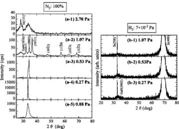
Figures 1共a兲 and 1共b兲 show the XRD patterns obtained in the -2 scan mode for the sputter-deposited GaN films on silicon substrates without and with the addition of hydrogen gas, respectively. The sputtering pressure was varied from 2.70 to 0.08 Pa in the case of Fig. 1共a兲 and from 1.07 to 0.27 Pa in the case of Fig. 1共b兲. The samples corresponding to the spectra in Fig. 1共b兲 were deposited under a hydrogen partial pressure of ⬃7⫻10−2Pa. The peaks observed at the lowest
position, 2= 28.4°, in Fig. 1共a兲 and those at 2= 33.0° and 69.1° in Fig. 1共b兲 originate from the 4°-off Si共111兲 and Si共100兲 substrates, respectively.
The XRD pattern in Fig. 1共a-1兲 shows no strong GaN peak. This indicates that the film deposited at 2.70 Pa is amorphous or amorphous-like in nature. The GaN film de-posited at 1.07 Pa 关Fig. 1共a-1兲兴, on the other hand, shows XRD pattern consisting of many peaks originating from vari-ous crystal planes of hexagonal 共␣-兲 GaN, such as 共101¯0兲,
共0002兲, and 共112¯0兲. These peak positions agree with those
reported on the Joint Committee on Powder Diffraction Stan-dards 共JCPDS兲 card of␣-GaN共Ref. 14兲. This indicates that the film deposited at 1.07 Pa is polycrystalline with mixed orientations of the crystalline planes. For the GaN films de-posited at 0.27–0.08 Pa 关Figs. 1共a-4兲 and 1共a-5兲兴, only the strong peak related to the␣-GaN共0002兲 plane is observed at around 2= 33°. These results suggest that the films depos-ited at low pressures have a highly preferred orientation 共c plane兲. Note that the XRD intensity observed in Fig. 1共a-4兲 is much stronger than the others.
The XRD pattern shown in Fig. 1共b兲 suggests that the GaN:H films are amorphous or amorphous-like. A very weak crystalline peak can be recognized in the low-angle region of the XRD pattern 共2⬃33.5°兲. This peak is due to GaN共0002兲 and becomes stronger with lower deposition pressures.
In order to examine whether the GaN films deposited in 100% nitrogen gas at low pressures are epilayers共i.e., single-crystalline layers兲, we performed reflection high-energy elec-tron diffraction共RHEED兲 observations of the film deposited at 0.27 Pa关Fig. 1共a-4兲兴. The RHEED pattern shows a streaky spot pattern, suggesting that the film is oriented along the c direction and that its surface is very smooth. However, no change in the RHEED pattern was observed after the rotation of the film around the c axis. This indicates that the GaN film is not single crystalline, but is highly oriented to the c axis.
B. Fourier transform infrared spectroscopy
Figure 2 shows the FTIR spectra obtained from 共a兲 ␣-GaN and 共b兲 GaN:H films sputter deposited on Si共100兲 substrates at 0.27 and 0.27–1.06 Pa, respectively. Only a vi-brational mode at around 555 cm−1is observed in Fig. 2共a兲.
This mode is caused by the GaN lattice absorption band and is observed in single-crystalline␣-GaN at around 533 cm−1
FIG. 1. XRD patterns for GaN films sputter deposited in nitrogen gas共a兲 without and共b兲 with hydrogen gas at a partial pressure of 7⫻10−2Pa. The
substrates used were 4°-off Si共111兲 and Si共100兲, respectively.
FIG. 2. FTIR absorption spectra for共a兲␣-GaN and共b兲 GaN:H films sputter deposited on Si共100兲 substrates at 0.27 Pa in 100% nitrogen gas and at 0.27–1.06 Pa in nitrogen/hydrogen mixed gas, respectively.
关E⬜c;A1共TO兲兴 and 560 cm−1 关E储c ; E1共TO兲兴. 15
The spectra shown in Fig. 2共b兲 show not only the GaN absorption band at
⬃555 cm−1, but also new peaks at⬃1000 and ⬃3200 cm−1.
It is clear that the hydrogen atoms introduced into GaN form hydrogen-related bonds with the host lattice atoms.
Note that the⬃3200 cm−1 absorption peak seen in Fig. 2共b兲 is composed of many hydrogen-related bonds, as dem-onstrated in Fig. 3. The primary N–H bonds peaking at 3210 and 3500 cm−1 may represent the N–H bond in GaNH3+ or
NH4+ molecules.16
The secondary peaks at 2990 and 3350 cm−1 represent the N–H bond in GaNH
2 or NH3
mol-ecules. The higher wave number peaks at 3500 and 3350 cm−1 can be considered to be due to N–H bonds that
are not bound to water molecules, while those at the lower wave numbers of 2990 and 3210 cm−1 may be bound with
water molecules. The latter peaks may, thus, be observed at lower wave numbers than the former.
In order to elucidate the effects of added hydrogen on the lattice absorption properties, we have prepared GaN:H films deposited with different amounts of hydrogen 共1–7
⫻10−2Pa兲 in the reactive gas at a constant sputtering
pres-sure共0.53, 0.80, or 1.06 Pa兲. Examples of FTIR absorption spectra obtained from these films are shown in Fig. 4 for
1.06 Pa. On the basis of these spectra and those shown in Fig. 2共b兲, we conclude that the hydrogen bond density is strongly dependent on the total sputtering pressure, but not on the hydrogen partial pressure.
C. Optical absorption
One of the most important parameters characterizing semiconductor properties is the band-gap energy Eg. In order
to determine the fundamental absorption edges of the sputter-deposited GaN and GaN:H films, we have measured optical absorption spectra of these films deposited on Corning 7059 glass.
The experimental absorption spectra ␣共E兲 measured at
T = 300 K for ␣-GaN and GaN:H films are shown in Figs. 5共a兲 and 5共b兲, respectively. The dependence of␣ on photon energy E can be written as
␣共E兲 = A共E − Eg兲n 共1兲
or, equivalently, ␣共E兲1/n= A1/n共E − E
g兲, 共2兲
where n = 1 / 2 and 2 correspond to the direct and indirect band gaps, respectively. It is known that crystalline GaN is a direct-band-gap semiconductor having a band-gap energy of
Eg⬃3.4 eV for ␣-GaN or ⬃3.2 eV for cubic 共-兲 GaN at room temperature.15 The plot shown in Fig. 5共a兲 gives the intercept at Eg= 3.38 eV on the energy axis. This value is nearly equal to that for single-crystalline␣-GaN共⬃3.4 eV兲. Kubota, Kobayashi, and Fujimoto11succeeded in the epitax-ial growth of hexagonal GaN films on sapphire substrates by rf-magnetron sputtering and measured their absorption spec-tra. The Eg value obtained by those authors was 3.21 eV, which is considerably smaller than any previously reported ␣-GaN value.
As mentioned before, the GaN:H films sputter deposited in a mixture of nitrogen and hydrogen gases are amorphous or amorphous-like. The optical transitions in amorphous semiconductors can be described, to a first approximation, by the “nondirect” transition model in which the conservation of energy, but not of the wavevector, is significant.17 The ab-FIG. 3. FTIR absorption spectra in the⬃3200 cm−1region of GaN:H films
sputter deposited on Si共100兲 substrates at 共a兲 0.27, 共b兲 0.53, and 共c兲 1.06 Pa in nitrogen gas mixed with hydrogen gas at a partial pressure of 7
⫻10−2Pa. The dashed lines represent the deconvolution of each spectrum
into several hydrogen-related peaks.
FIG. 4. FTIR absorption spectra for GaN:H films sputter deposited at 0.27 Pa on Si共100兲 substrates in nitrogen gas mixed with hydrogen gas at a partial pressure of 1⫻10−2or 7⫻10−2Pa.
FIG. 5.共a兲 Plots of 共␣E兲2vs photon energy E for␣-GaN film at 300 K and
共b兲 those of 共␣E兲1/2vs E for GaN:H film at 300 K. The␣-GaN and GaN:H
films were sputter deposited at 0.27 Pa on Corning 7059 glass in 100% nitrogen gas and in nitrogen/hydrogen mixed gas, respectively.
sorption coefficient in this case can be given by almost the same expression as that for the indirect transitions in crystal-line semiconductors, i.e., Eq.共1兲 with n=2. The optical ab-sorption data obtained from the GaN:H film are plotted in Fig. 5共b兲 as␣1/2vs E. From this plot, we obtain Eg⬃3.7 eV.
This value is much larger than those for crystalline GaN
共⬃3.4 eV for ␣-GaN or ⬃3.2 eV for -GaN兲. Indeed, we can clearly see the oscillations in the␣共E兲 spectra for E up to 3.7 eV. Note that these oscillations originate from the mul-tiple internal reflections of light in the sputter-deposited GaN films where the films are effectively transparent.
D. Photoluminescence 1. GaN film
Figure 6 shows the PL spectra measured at T = 14, 45, and 60 K for a GaN film sputter deposited on Si共100兲 sub-strates in a pure nitrogen atmosphere of 0.27 Pa. These spec-tra can be resolved into five peaks centered at⬃2.1, ⬃2.3,
⬃2.7, ⬃3.0, and ⬃3.3 eV, as determined from a Gaussian
line shape fit. The⬃3.3 eV peak may correspond to the edge or donor-acceptor pair emission, but is not sharp even at low temperature. The yellow emission band at ⬃2.3 eV is often observed in ␣-GaN. A description of the luminescent prop-erties of GaN has been given by Akasaki and Amano18 and Leroux and Gil19 who reviewed some of the work done on undoped and doped GaN crystals.
We have observed PL emission only at temperatures lower than ⬃100 K. Some authors have observed PL,20–22 cathodoluminescence,20 and electroluminescence23,24 from “rare-earth-activated” GaN films deposited by sputtering. Note that rare-earth elements, such as Er and Tm, may be incorporated into semiconductors as an optically active in-clusion, not strictly as dopants.
2. GaN:H film
As mentioned above, PL emission from the sputter-deposited crystalline GaN film is very weak and observed only at low temperatures共T⬍100 K兲. On the other hand, we have observed relatively strong PL emission from GaN:H film even at high temperatures. In Fig. 7, we show, as an example, the PL spectrum for GaN:H film measured at T = 300 K. The film was sputter deposited onto a Si共100兲 sub-strate at 0.27 Pa of nitrogen gas mixed with hydrogen gas at a partial pressure of 7⫻10−2Pa. For comparison, the PL
spectrum taken from a single-crystalline ␣-GaN film is shown in Fig. 7 by the dashed line. This film was grown epitaxially using trimethylgallium and ammonium in a verti-cal MOCVD reactor on a 共0001兲 sapphire substrate at 1040 °C after depositing a GaN nucleation layer at 600 °C for 60 s.
The PL emission from the sputter-deposited GaN:H film shows a single emission peak, Eed0, at ⬃3.25 eV. On the
other hand, the MOCVD-grown ␣-GaN film exhibits an emission at ⬃3.4 eV and a deep yellow emission at
⬃2.3 eV. Note that the GaN:H film is evaluated to be
pre-dominantly amorphous 关Fig. 1共b兲兴 and has the relatively large band-gap energy of ⬃3.7 eV 关Fig. 5共b兲兴. Furthermore, the ⬃3.25 eV 共Eed0兲 emission shown in Fig. 7 is relatively
intense, about half that of the ⬃3.4 eV emission in the MOCVD-grown␣-GaN film, and sharp. It is, thus, very dif-ficult to consider that the ⬃3.25 eV peak observed in the GaN:H film originates from the amorphous GaN matrix. The peak is, therefore, considered to be due to crystalline GaN particles embedded in the amorphous GaN matrix. An emis-sion from nanoscale ZnSe particles embedded in amorphous ZnSe has also been reported by Lee et al.25
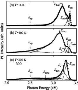
Figure 8 shows the PL spectra for GaN:H film taken at 14–300 K. It is seen that the GaN:H film exhibits very com-plex luminescent properties, i.e., its spectra are strongly de-pendent on temperature T. This is particularly obvious around T⬃180 K, as shown in the enlargement in the inset of Fig. 8. A single peak is observed for T from 300 K down to⬃220 K, below which new peaks appear in the band-edge region and in the donor-acceptor 共DA兲 pair and deep-emission regions. The PL intensity is also found to increase with decreasing T.
FIG. 6. PL spectra for␣-GaN film sputter deposited on the Si共100兲 substrate at 0.27 Pa in 100% nitrogen gas, measured at共a兲 14, 共b兲 45, and 共c兲 60 K. The light solid lines represent the deconvolution of each spectrum into sev-eral Gaussian emission peaks. Note that the intensity scales in共a兲-共c兲 are all the same units; then, the relative intensity of the three PL can be directly compared.
FIG. 7. Room-temperature PL spectrum for GaN:H film deposited on the Si共100兲 substrate at 0.27 Pa in nitrogen gas mixed with hydrogen gas at a partial pressure of 7⫻10−2Pa. For comparison, the PL spectrum for a
single-crystalline␣-GaN film grown on a共0001兲 sapphire substrate by MOCVD is shown by the dashed line in reduced scale of⫻共1/2兲.
By performing Gaussian line shape analysis, our mea-sured PL spectra can be resolved into several peaks. We show in Fig. 9 the results of such analysis. For T = 14 K, the analysis reveals two edge-emission peaks at 3.363 eV共Eed0兲
and 3.315 eV共Eed1兲, a DA-pair emission at 3.199 eV 共EDA1兲,
and a very weak deep emission at⬃2.5 eV 共Edp兲. The
indi-vidual contributions of each emission peak or band to the PL spectra are indicated in Figs. 9共a兲–9共c兲 by the light solid lines. Here, we assumed that the DA-pair emission intensity can be simply written, using a Gaussian function, as26
IDA1共E兲 =
兺
n=0
⬁
SDA1n exp
冋
−关E − 共EDA10
− nqLO兲兴2
⌫2
册
, 共3兲where EDA10 is the zero-phonon共n=0兲 emission energy, SDA1n is the strength of the nth phonon emission line, qLOis the
longitudinal optical共LO兲 phonon energy 共92 meV; Ref. 15兲, and⌫ is the broadening parameter. As the impurity 共donor or acceptor兲 energy increases, the interaction of the electron with lattice vibrations or the electron-phonon coupling
be-comes stronger. In this particular case, LO phonon coupling is by far the strongest because of the polarization field asso-ciated with it. For the shallow hydrogenic impurity centers, phonon coupling is weak and often only one LO phonon replica 共n=1兲 can be observed. For deeper centers, phonon coupling is much stronger, and three or more LO phonon replicas can often be recognized. Theoretically, the intensity
IDA1in Eq.共3兲 is given by a Poisson distribution function 26
SDA1n ⬀ exp共− N¯兲N ¯n
n!, n = 0,1,2,…, 共4兲
where N¯ is the mean number of emitted phonons.
At higher temperatures, the edge-emission peaks become considerably broader and new emission peaks, labeled Ex
and EDA2, appear at⬃3.2 and ⬃2.9 eV, respectively. As
ex-pected, the line shape of IDA1共EDA1兲 expressed by Eq. 共3兲 is
strongly asymmetric and has a tail on the low-photon-energy side关see Figs. 9共a兲 and 9共b兲兴.
We show, in Fig. 10, the temperature variation of each peak energy in the PL emission spectra of GaN:H film. For comparison, the temperature dependence of the excitonic en-ergy gap Egin single-crystalline␣-GaN, taken from Ref. 15,
is plotted by the heavy dashed line.
Conventionally, the temperature variation of the band-gap energy is expressed by Varshni’s formula27
Eg共T兲 = Eg共0兲 −
␣T2
T +, 共5兲
where Eg共0兲 is the band-gap energy at T=0 K,␣ is in
elec-tron volts per Kelvin, and is closely related to the Debye temperature Dof the material共in Kelvin兲. The heavy solid
line in Fig. 10 represents the fitted result of Eq. 共5兲 to the experimental data of Eed0共T兲. The fit-determined parameters
are Eed0共0兲=3.363 eV, ␣= 10.0⫻10−4eV/ deg, and 
= 850 K. FIG. 8. PL spectra for GaN:H film measured at T from 14 to 300 K. The
GaN:H film was sputter deposited at 0.27 Pa on the Si共100兲 substrate in nitrogen gas mixed with hydrogen gas at a partial pressure of 7⫻10−2Pa.
The inset shows the PL spectra between T = 140 and 220 K.
FIG. 9. PL spectra for GaN:H film measured at共a兲 14, 共b兲 100, and 共c兲 300 K. The GaN:H film was sputter deposited at 0.27 Pa on the Si共100兲 substrate in nitrogen gas mixed with hydrogen gas at a partial pressure of 7
⫻10−2Pa. Individual contributions to the PL intensity from each emission
peak or band are shown by the light solid lines.
FIG. 10. PL peak energies plotted as a function of temperature T for GaN:H film sputter deposited at 0.27 Pa on the Si共100兲 substrate in nitrogen gas mixed with hydrogen gas at a partial pressure of 7⫻10−2Pa. For
compari-son, the temperature dependence of the excitonic energy gap Egin single-crystalline␣-GaN, taken from Ref. 15, is shown by the heavy dashed line. The heavy solid line represents the fitted result of Eq.共5兲 to the experimen-tal Eed0共T兲.
The characteristic temperature of= 850 K determined here is equal to the Debye temperature D⬃820–874 K at
T = 300–2000 K for ␣-GaN.15 It is also found that  is roughly equal to the effective LO phonon temperature of
⬃1070 K obtained from k= qLO 共⬃92 meV兲. This
sug-gests that the major contribution to the temperature variation of Eed0 is from the optical phonons. The temperature varia-tion, −5⫻10−4ev/ deg, for E
DA2in Fig. 10 is equal to that of
the excitonic energy gap, −共3.6–5.3兲⫻10−4ev/ deg, observed
for single-crystalline ␣-GaN 共Ref. 15兲. It should be noted, however, that Eed1 and Exshow no strong dependence on T.
As a result, Eed0and Eed1cross at T⬃250 K. Above 250 K,
these two peaks are observed as a single broad peak 关Fig. 9共c兲兴. Unfortunately, the origins of Eed1and Exare not clear
at present.
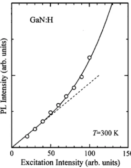
Finally, we show, in Fig. 11, the laser-power dependence of the PL emission intensity for Eed0measured at T = 300 K.
The integrated PL intensity I versus laser power Iex can be
simply written as I⬀共Iex兲␥, where the dimensionless
expo-nent ␥ is known to be 1⬍y⬍2 for free-exciton or bound-exciton emission and y艋1 for free-to-bound or DA-pair emission.28 Our experimental data indicate that at low exci-tation levels, the exponential parameter ␥ is unity, but at higher levels, the emission intensity I increases superlinearly with Iex. The observed superlinearity may arise from the
ef-fects of fine GaN particles embedded in the amorphous GaN matrix.
IV. CONCLUSIONS
We deposited GaN films by reactive rf-magnetron sput-tering in a nitrogen gas without and with the addition of hydrogen gas. The XRD patterns suggested that the GaN films sputter deposited in nitrogen gas at pressures lower than 0.53 Pa without hydrogen gas are polycrystalline films with the 共0001兲 texture, while those deposited at or above
was observed from the sputter-deposited ␣-GaN film at T
⬍100 K and found to show five emission bands centered in
the ⬃2.1–3.3 eV spectral region. The amorphous GaN:H film showed a relatively strong PL emission even at room temperature. The T = 14 K spectrum exhibited two edge emissions at 3.363 and 3.315 eV, a DA-pair emission at 3.199 eV, and a very weak deep emission at⬃2.5 eV. The PL emission observed in the GaN:H film may originate from crystalline GaN particles embedded in the amorphous GaN matrix.
ACKNOWLEDGMENTS
This work was supported in part by Gunma University-Satellite Venture Business Laboratory共GU-SVBL兲 and by a Grant-in-Aid for Scientific Research 共C兲 from the Ministry of Education, Culture, Sports, Science and Technology, Ja-pan.
1
See, for example, S. Nakamura and G. Fasol, The Blue Laser Diode
共Springer, Berlin, 1997兲.
2
See, for example, J. H. Edger, S. Strite, I. Akasaki, H. Amano, and C. Wetzel, Properties, Processing and Applications of Gallium Nitride and
Related Semiconductors共INSPEC, London, 1999兲, pp. 357–453.
3
H. J. Hovel and J. J. Cuomo, Appl. Phys. Lett. 20, 71共1972兲.
4
J. C. Vesely, M. Shatzkes, and P. J. Burkhardt, Phys. Rev. B 10, 582
共1974兲.
5
N. Puychevrier and M. Menoret, Thin Solid Films 36, 141共1976兲.
6
E. Lakshmi, B. Mathur, A. B. Bhattacharya, and V. P. Bhargava, Thin Solid Films 74, 77共1980兲.
7
K. Matsushita, Y. Matsuno, T. Hariu, and Y. Shibata, Thin Solid Films 80, 243共1981兲.
8
T. L. Tansley and R. J. Egan, Thin Solid Films 164, 441共1988兲.
9
T. Miyazaki, T. Fujimaki, S. Adachi, and K. Ohtsuka, J. Appl. Phys. 89, 8316共2001兲.
10
T. Hariu, T. Usuba, H. Adachi, and Y. Shibata, Appl. Phys. Lett. 32, 252
共1978兲.
11
K. Kubota, Y. Kobayashi, and K. Fujimoto, J. Appl. Phys. 66, 2984
共1989兲.
12
J. Ross, M. Rubin, and T. K. Gustafson, Mater. Res. Soc. Symp. Proc. 242, 457共1992兲.
13
T. Miyazaki, M. Kunugi, Y. Kitamura, and S. Adachi, Thin Solid Films 287, 51共1996兲.
14
JCPDS共Joint Committee on Powder Diffraction Standards兲 No. 2-1078
共1991兲.
15
S. Adachi, Handbook on Physical Properties of Semiconductors Volume 2:
III-V Compound Semiconductors共Kluwer, Boston, 2004兲.
16
L. J. Bellamy, The Infra-red Spectra of Complex Molecules 共Methuen, London, 1958兲.
17
S. Adachi, Phys. Rev. B 43, 12316共1991兲.
18
I. Akasaki and H. Amano, in Properties of Group III Nitrides, edited by J. H. Edgar共INSPEC, London, 1994兲, p. 222.
19
M. Leroux and B. Gil, in Properties, Processing and Applications of
Gal-lium Nitride and Related Semiconductors, edited by J. H. Edger, S. Strite,
I. Akasaki, H. Amano, and C. Wetzel共INSPEC, London, 1999兲, p. 58.
20
H. Chen, K. Gurumurugan, M. E. Kordesch, W. M. Jadwisienczak, and H. FIG. 11. Excitation laser-power dependence of the PL intensity for GaN:H
at T = 300 K. The GaN:H film was sputter deposited at 0.27 Pa on the Si共100兲 substrate in nitrogen gas mixed with hydrogen gas at a partial pres-sure of 7⫻10−2Pa. The open circles represent the experimental data, while
the solid line is drawn through the data as a guide to the eye. The dashed line indicates the relation of I⬀共Iex兲␥with␥= 1.