Study on novel fabrication processes of AlN by
pulsed DC reactive sputtering and substitution
reaction
著者
マルセティオ ノープラジュダ
学位授与機関
Tohoku University
Study on novel fabrication processes of AlN
by pulsed DC reactive sputtering and substitution reaction
(反応性パルス DC スパッタ法と置換法による AlN 結晶の新規
作製プロセスに関する研究)
by:
Marsetio Noorprajuda
B7GD1509
A Dissertation Presented in Partial Fulfillment of the Requirements for the Degree Doctor of Philosophy
Approved July 2020 by the Graduate of Supervisory committee: Hiroyuki Fukuyama
Makoto Ohtsuka
Masayoshi Adachi
Environmental Studies for Advance Society Graduate School of Environmental Studies
Tohoku University 17th July 2020
Table of content
Table of content ... 2
Chapter 1 Introduction ... 4
1.1 Background ... 4
1.1.1 Optical devices - UV-LEDs ... 4
1.1.2 Power devices - GaN HEMT ... 5
1.2 AlN Properties ... 7
1.3 Fabrication Methods of AlN Film on Sapphire... 10
1.3.1 Metal-Organic Vapour-Phase Epitaxy (MOVPE) ... 10
1.3.2 Hydride Vapour Phase Epitaxy (HVPE) ... 11
1.3.3 Pulsed Laser Deposition (PLD) ... 11
1.3.4 Sputtering ... 11
1.3.5 Molecular Beam Epitaxy (MBE) ... 12
1.3.6 Liquid Phase Epitaxy (LPE) ... 12
1.3.7 Comparison of Fabrication Methods of AlN Film on Sapphire ... 13
1.4 Fabrication Methods of AlN bulk crystal ... 14
1.4.1 Physical Vapour Transport (PVT) ... 14
1.4.2 Hydride Vapour Phase Epitaxy (HVPE) ... 14
1.4.3 Other Fabrication Methods of AlN Bulk ... 15
1.5 Objectives and Novelty of Research ... 16
1.5.1 Pulsed DC Reactive Sputtering Method forming AlN film on sapphire ... 16
1.5.2 Substitution method forming AlN bulk crystal ... 16
References ... 16
Chapter 2 Pulsed DC Reactive Sputtering ... 22
2.1 Introduction ... 22 2.2 Principle ... 24 2.3 Experimental ... 24 2.3.1 Materials ... 24 2.3.2 Sputtering condition ... 24 2.3.3 Characterization ... 25 2.3.4 Annealing condition ... 26 2.4 Results ... 28
2.4.1 Effect of oxygen addition on polarity and residual stress of AlN films ... 28
2.4.2 Effect of thickness on crystalline quality and residual stress of AlN films ... 50
2.4.3 Annealing of AlN films... 55
2.5 Discussion ... 101
2.5.1 Modelling of oxygen addition into AlN films ... 101
2.5.2 Annealing of AlN films... 104
2.6 Conclusion ... 110
References ... 111
Chapter 3 Substitution Reaction Experiment ... 113
3.1 Introduction ... 114
3.2 Principle ... 115
3.3 Experimental ... 116
3.3.1 Sample Preparation ... 116
3.3.2 Thermogravimetry–Differential Scanning Calorimetry ... 116
3.3.3 Substitution Reaction Experiment ... 116
3.3.4 Characterization ... 118
3.4 Results ... 119
3.4.1 Thermogravimetry–Differential Scanning calorimetry ... 119
3.4.2 Cu Heating Experiment for Equipment Calibration ... 119
3.4.3 Substitution Reaction Experiment ... 120
3.5 Discussion ... 165
3.5.1 Growth model of substitution reaction method ... 165
3.5.2 Kinetics of AlN growth ... 166
3.5.3 Effect of polarity of GaN substrate on AlN formation... 169
3.6 Conclusion ... 170
References ... 171
Chapter 4 Conclusion ... 172
Chapter 1 Introduction
1.1 Background
1.1.1 Optical devices - UV-LEDs
Ultraviolet light emitting diodes (UV-LEDs) are expected to be used in a wide variety of applications as illustrated in Fig. 1.1. UV-LEDs can be used for wide range applications including white light illumination1.1, microorganism disinfection1.2, pollutants removal1.3, skin curing1.4, vitamin D generation1.5, antioxidant enrichment1.6, and virus suppression1.7. UV-LED
is expected to have higher quantum efficiency as the technology continues to advance. Recently, aluminum gallium nitride (AlGaN)-based UV-LED is being developed because of its bandgap range from 3.4 eV for GaN to 6.0 eV1 for AlN for wide range of applications. Moreover, AlGaN offers high external quantum-efficiency and is environmental friendly material (no hazardous components). Thus, AlGaN is promising material for UV-LED as optical device. Aluminium nitride (AlN) is a good candidate for a substrate of AlGaN-based UV-LED owing to its wide bandgap (above 6 eV)1.8, UV transparency1.9,and close lattice constant with that of AlGaN.1.10 AlGaN UV-LED can be fabricated by depositing AlGaN on AlN film on sapphire1.11 or directly on AlN bulk1.12 (see fig. 1.2). Fabricating AlGaN UV-LED by depositing AlGaN on AlN film on sapphire may lead to low cost. Depositing AlN film on a sapphire substrate has been fabricated by several methods, such as metal-organic vapour-phase epitaxy (MOVPE)1.13,1.14,
hydride vapour phase epitaxy (HVPE)1.15,1.16, pulsed laser deposition (PLD)1.17,1.18, molecular beam epitaxy (MBE) 1.19,1.20, or sputtering1.21,1.22. However, the crystalline quality of AlN film on the sapphire substrate is often low owing to a large lattice misfit between AlN and sapphire. On the other hand, high crystalline quality of AlN leads to high external quantum efficiency of AlGaN-based UV-LED.1.12 Thus, improving crystalline quality of AlN film is important for good AlGaN UV-LED performance. The performance of AlGaN UV-LED also improved by depositing AlGaN on AlN bulk owing to high crystalline quality of AlGaN on AlN bulk because of close lattice constants between AlGaN and AlN bulk. 1.12 The AlN bulk crystal has been mostly grown through physical vapour transport (PVT)1.23,1.24 and HVPE1.25,1.26. The PVT
technique enables AlN bulk crystal growth with high AlN growth rate.1.27,1.28 However, the
PVT technique requires a high growth temperature of approximately 2373 K, which can generate cracks or thermal etch pits owing to high tensile residual stress exist in AlN.1.29,1.30 On the other hand, HVPE technique requires PVT-AlN substrates to obtain high crystalline quality AlN. Therefore, it seems no further developments can be made in the common AlN fabrication technologies. Lowering the temperature of AlN bulk manufacturing process is important to achieve high crystalline quality of AlN with low tensile residual stress to prevent cracks or thermal etch pits. Thus, the high-crystalline quality of AlN stress can be obtained from 2 approaches: improving the crystalline quality of AlN film on sapphire substrate or lowering the temperature processing of AlN bulk fabrication method.
Fig. 1.1 Wide range applications of UV-LED.
Fig. 1.2 AlGaN UV-LED can fabricated by depositing AlGaN on AlN film on Sapphire or directly on
AlN bulk.
1.1.2 Power devices - GaN HEMT
A high-electron-mobility transistor (HEMT), is a field-effect transistor incorporating a junction between two materials with different band gaps. In GaN HEMT case, the material combination is GaN with AlGaN (see Fig. 1.3 GaN HEMT) are recently widely used in many fields such as solar and wind turbine inverter1.31, Inverter and DC-DC converter in the future Japan AGV car1.32, amplifier in military radar1.33, and amplifier for LTE (4G)1.34 as illustrated in Fig. 1.4. GaN HEMT has advantage for high power and high frequency compared to other devices such as SiC metal–semiconductor field-effect transistor (MESFET) or GaAs HEMT (see Fig. 3). The typical GaN HEMT structure on Si and AlGaN HEMT on AlN bulk are shown in Fig. 2.
AlN film is often used as a buffer layer in GaN HEMT structure to improve GaN crystalline quality that leads to high electron mobility of two-dimensional electron gas (2DEG) for fast switching.1.35 To meet the high demand of high power, high frequency, and fast switching power device, the next generation of GaN HEMT is expected. High breakdown voltage and low resistance is required for high power, high frequency, and fast switching power device. The breakdown voltage and resistance of some semiconductor materials is summarized in Baliga figure of merit (BFOM) in Fig. 1.5. “Baliga figure of merit (BFOM) is defined as
VBR/RON-SP. Here, VBR is the breakdown voltage (maximum voltage the switch can block when
off), and RON-SP is the specific on-resistance (inverse of conductance per area when on).”1.36
The bottom-right-corner of BFOM indicated the improving performance of material. From that figure, AlN bulk is expected to be the future material as substrate for AlGaN HEMT for next generation of high power, high frequency, and fast switching power device. In addition, AlN is good candidate substrate for AlGaN HEMT owing to its close lattice constant with AlGaN. As mentioned before in this subsection, improving the crystalline quality may lead to high electron mobility of two-dimensional electron gas (2DEG) for fast switching.1.35 Therefore,
high crystalline quality AlN bulk fabrication method is required to produce AlN bulk substrate for AlGaN HEMT. As mentioned in the subsection 1.1.1 optical devices – UV LEDs, the common AlN bulk fabrication method, PVT technique, requires a high growth temperature of approximately 2473 K, which can generate cracks or thermal etch pits owing to high tensile residual stress exist in AlN.1.29,1.30 Accordingly, low the temperature of AlN bulk manufacturing process is important to achieve high crystalline quality of AlN with low tensile residual stress to prevent cracks or thermal etch pits. Thus, the high-crystalline quality of AlN can be obtained by low temperature processing of AlN bulk fabrication method.
Fig. 1.4 Wide range applications of GaN HEMT.
Fig. 1.5 Wide range applications of UV-LED.
1.2 AlN Properties
The crystal structure of AlN is wurtzite. Fig. 1.6 shows the schematic of an AlN crystal structure showing a-plane and c-plane of AlN and lattice constant a and c. There are two different kind of polarity of AlN crystal structure. One is N-polar and the other is Al-polar. Figure 1.7 shows the schematic of two different kind of polarity of AlN. The N-polar can be seen with nitrogen atom below the aluminum atom. In contrast, the Al-polar is shown with aluminum atom just below the nitrogen atom. N-polar AlN has high charge carriers as in (Al)GaN/AlN HEMT structure which is advantageous for fast switching power device. 1.37 On the other hand, the Al-polar AlN exhibits smooth surface morphology and high growth rate of AlN. 1.38,1.39
Fig. 1.6 Schematic of an AlN crystal structure showing a-plane and c-plane of AlN.
N-polar Al-polar
High charge carriers Smooth Surface
High growth rate
In our laboratory, the “sapphire nitridation” method has been developed to obtain AlN on sapphire.1.40 The nitrided sapphire has high crystalline quality of AlN and N-polarity. However,
the thickness is only about 10 nm. To obtain thick AlN film, high growth rate of Al-polar AlN is needed. Thus, the polarity inversion of N-polar AlN after sapphire nitridation method is attempted in chapter 2. Moreover, the high crystalline quality and polarity of AlN film on the sapphire substrates is important for improving device performance. Aluminum polar AlN film is necessary to obtain a smooth surface1.41 AlN for substrate of heteroepitaxial growth of AlGaN. Therefore, various methods have been attempted to control the polarity of the AlN film on the sapphire substrate1.42–1.44, including modifying the initial growth conditions such as using very low V/III ratio, Al-source/N source pulsed flow, or Al-source pre-flow in the metal organic vapor phase epitaxy (MOVPE) method. The polarity inversion of AlN was also done by varying the oxygen partial pressure in liquid phase epitatxy (LPE) method1.45. In case of GaN film, the polarity control is done by inserting an interlayer of composite AlN/aluminum oxide (AlOx) or MgxNy on an N-polar GaN film using MBE method1.46–1.48. The polarity inversion technique which is simple and applicable for sputtering technique is by varying the oxygen partial pressure of the mixture gases.
Some physical and thermodynamic properties of AlN together with other semiconductor materials are shown in table 1. Aluminium nitride (AlN) has wide bandgap (6 eV) and close lattice constant with that of AlGaN. Thus, it is a good candidate for a substrate of AlGaN-based UV-LED. Moreover, as discussed in subsection 1.1.2 Power device - GaN HEMT, AlN located in the bottom-right-corner of BFOM and has high BFOM relative to Si value. For this reason, AlN is the next generation of GaN HEMT. Therefore, the development of low-cost, high-quality AlN fabrication method of is important. The common AlN fabrication methods will be reviewed in next subsections to approach the development of low-cost, high-quality AlN fabrication methods.
Table 1.1 Some physical and thermodynamic properties of AlN together with other semiconductor materials.
1.3 Fabrication Methods of AlN Film on Sapphire
1.3.1 Metal-Organic Vapour-Phase Epitaxy (MOVPE)
In the MOVPE, AlN is produced by reacting of the precursors, typically trimethylaluminum (TMAl) and ammonia on a heated substrate, following the reaction:
Al(CH3)3 + NH3 → AlN + 3CH4
The reaction at high temperature of 1423–1573 K1.49–1.51 can induce a parasitic reaction that result a complex gas phase such as Al(CH3)2•NH2 and inhibit the AlN crystallization resulting
low AlN growth rate.1.52 The range of the AlN growth rate of MOVPE method is 0.06-0.4 µm/h.1.49–1.51 The screw dislocation density is 4.9×10⁷–1.3×1010 cm−2 1.49–1.51 and the edge dislocation density is 9×10⁹–1.3×1010 cm−2.1.49–1.51
The critical issue of heteroepitaxial growth is high dislocation density often unintentionally generated owing to lattice mismatch between sapphire substrate and AlN. As mentioned by Susilo et al.1.22, high screw and edge dislocation densities above 1×109 cm2 is not sufficient for UVC-LEDs because of low external quantum efficiencies (EQE). Thus, many efforts have been accomplished to reduce the dislocation densities in MOVPE-AlN, including 2-dimensional growth mode (7×108 cm-2 for screw dislocation and 2×109 cm-2 for edge dislocation)1.53, modified Migration-enhanced epitaxy (MEE)1.54 with estimated screw dislocation density of 4.0×106 cm−2 and edge dislocation density of 5.0×107 cm−2, epitaxial lateral overgrowth (ELO) by using patterned AlN as a template (8.0×107 cm−2 for screw dislocation and 1.2×108 cm-2 for edge dislocation)1.55, NH
3 pulse-flow growth (the screw and
edge dislocation densities of AlN layer were 3.8×107 cm-2 and 7.5×108 cm-2)1.56, and annealing estimated screw dislocation density of 1×108 cm−2 and edge dislocation density of 5×108 cm−2.1.57
Materials
Properties Si SiC GaN AlN
Bandgap energy, Eg (eV) 1.1 3.3 3.4 6.0
Breakdown field, Ec (MV cm -1 ) 0.3 3 4 15 Lattice constant, a (nm) 0.5430 0.3080 0.3189 0.3111 Thermal conductivity, λ (W cm-1 K-1) 1.4 3.7 1.3 3.4
Thermal coefficient along a -axis, α (10-6 K) 3.6 4.3 6.2 6.9
1.3.2 Hydride Vapour Phase Epitaxy (HVPE)
In HVPE, AlN is fabricated by reacting the AlCl3 and ammonia precursors on a heated sapphire
substrate at high temperature of 1723 - 1773 K, following the reaction:
AlCl3 + NH3 → AlN + 3HCl
The AlN Growth rate is around 10-20 µm/h.1.58,1.59 The screw dislocation density is 4.9×10⁷– 1.2×1011 cm−21.58,1.59 and the edge dislocation density is 5.7×10⁸–1.6×1011 cm−2. 1.58,1.59
1.3.3 Pulsed Laser Deposition (PLD)
In this growth technique, the AlN film is grown either by the direct laser ablation of an AlN target with a laser beam using a nitrogen plasma, following reaction:
AlN → AIN
PLD often conducted at low AlN growth temperature of around 773–1173K.1.60,1.61 However, the AlN growth rate is quite low of 0.1 µm/h.1.61 The screw dislocation density is 1.5×10¹⁰–
8.1×1010 cm−21.60,1.61 and the edge dislocation density is 3.0×10¹⁰–1.2×1011 cm−2. 1.60,1.61
1.3.4 Sputtering
In sputtering method, AlN is fabricated by nitridation reaction of sputtered Al atom in Ar-nitrogen mixture gas just before deposition on the heated sapphire substrate, following reaction:
Al + 1/2N2 → AIN
The growth temperature is in the range of 573 and 823 K.1.62–1.66 The growth rate using RF
power is 0.5–2.9 µm/h1.62,1.63, using DC power is 1.5 µm/h1.64, using pulsed DC power is 0.3– 5 µm/h.1.65,1.66 The screw dislocation density and the edge dislocation density using RF power
are 4.9×10⁷–2.8×108 cm−21.62,1.63 and 4.9×109 cm−2 1.62,1.63, using DC power are 4.9×108 cm−2
1.64 and 1.6×1010 cm−2 1.64, using pulsed DC power are 5.2×10⁸–7.0×109 cm−2 1.65,1.66 and
1.5×10¹⁰–4.0×1010 cm−2.1.65,1.66
DC or RF reactive sputtering is commonly used to deposit AlN on the substrate due to its high reproducibility, low cost, and simplicity. However, sputtering with DC power source can cause arcing (abnormal electric discharge) which can poison the target and damage both the target and deposited film. On the other hand, sputtering with RF power source takes longer time to deposit AlN due to the lower deposition rate. The pulsed DC reactive sputtering suppresses the
arcing with interrupting the negative voltage in cathode (Al taget) so the fully dense film can be obtained.
Recently, annealing techniques have been demonstrated to improve the crystalline quality of AlN films. During the annealing, the columnarstructure AlN films coalesced and the domain boundaries annihilated. Thus, crystallinity of the AlN films improved.1.67
1.3.5 Molecular Beam Epitaxy (MBE)
In MBE, the Al atom and nitrogen gas (from the dissociation of ammonia precursor) are introduced from effusion cells to the heated substrate at 873-1273 K1.68 following reaction:
Al + 1/2N2 → AIN
The AlN growth rate is 0.1–0.31.68,1.69 The screw dislocation density is 1.5×10¹⁰–2.5×10¹⁰
cm−21.68 and the edge dislocation density is 10×1010–20×1010 cm−2.1.68
1.3.6 Liquid Phase Epitaxy (LPE)
In LPE, the AlN film is grown on sapphire substrate from the dissolved nitrogen and Al melt in the flux system for example Ga-Al solution1.70 or Al-Sn flux1.71, following reaction:
Al + 1/2N2 → AIN
The AlN growth temperature range from 1273–1573 K.1.70,1.71 The AlN growth rate is 0.2 µm/h.1.70 The screw dislocation density is 4.9×107 cm−21.70 and the edge dislocation density is 4×10⁸–1.1×109 cm−2. 1.70,1.71
1.3.7 Comparison of Fabrication Methods of AlN Film on
Sapphire
Table 1.2 Comparison of fabrication methods of AlN film on sapphire.
Table 1.2. summarize the AlN fabrication methods of AlN film on sapphire substrate. The critical issue of heteroepitaxial growth is high screw and edge dislocation densities often unintentionally generated owing to lattice mismatch between sapphire substrate and AlN. However, for the application of UVC-LEDs, low dislocation densities in AlN below 1×109 cm2 are required for high external quantum efficiencies (EQE) of UVC-LEDs.1.22 Moreover, the large different of thermal expansion coefficients along the a-axis of AlN (5.3×10⁻⁶ K−1) and sapphire (7.3×10⁻⁶ K−1)1.72 led to the excessive compressive stress and peeling off or exfoliation of the AlN during substrate cooling when fabricating AlN at high temperature. The compressive stress in AlN generated because the sapphire substrates tended to shrink more than the AlN during substrate cooling. Thus, low growth temperature is desirable to prevent peeling off or exfoliation of AlN. Among fabrication methods of AlN film on sapphire, sputtering is advantageous because it is often accomplished at low temperatures. In the term of AlN growth rate, MOVPE, PLD, MBE and LPE methods have low AlN growth rates. HVPE method offer high AlN growth rate. However, it requires high AlN growth temperature of 1773 K and hazardous AlCl3 precursors. From point of view of simplicity, sputtering, MBE and LPE
offer simple starting materials of Al and nitrogen gas. However, the AlN growth rates of MBE and LPE methods are low. Sputtering offers a low AlN growth temperature, simple, and environmentally friendly for AlN film on sapphire fabrication methods owing to its low temperature (823 K) and requirement of no hazardous chemicals (only Al and nitrogen). In sputtering, RF reactive sputtering has low AlN growth rate. DC reactive sputtering offer higher AlN growth rate than that using RF reactive sputtering. However, in DC reactive sputtering, arcing (abnormal electric discharge) often occurs and leads to low AlN growth rate. Pulsed DC reactive sputtering offer high AlN growth rate (3.6 µm/h can be achieved) among the sputtering techniques. However, the improvement of crystalline qualities of AlN is still required in pulsed DC reactive sputtering technique. For those reasons, the pulsed DC reactive sputtering method is being studied in chapter 2.
1.4 Fabrication Methods of AlN bulk crystal
1.4.1 Physical Vapour Transport (PVT)
Using PVT method, AlN is fabricated by sublimation of AlN crystal source (obtained by multiple sublimation recrystallization or sintered of AlN powder) and recrystallization at AlN seed in a nitrogen atmosphere, following reaction:
Al + 1/2N2 → AIN
The growth temperature is around 2273–2523 K.1.73,1.74 The AlN growth rate is 150–200 μm h−11.73,1.74
1.4.2 Hydride Vapour Phase Epitaxy (HVPE)
In HVPE, AlN is fabricated by reacting the AlCl3 and ammonia precursors on a heated substrate,
following the reaction:
AlCl3 + NH3 → AlN + 3HCl
AlN film fabricated on sapphire at high temperature of 1373 - 1773 K.1.75 The AlN Growth rate is around 85 µm/h.1.75
1.4.3 Other Fabrication Methods of AlN Bulk
The PVT technique requires a high growth temperature of approximately 2473 K, which consumes a lot of energy and can be expensive. By lowering the growth temperature, high-quality AlN can be achieved with a reasonable cost. The HVPE technique is usually conducted at a temperature below that of the PVT. However, the HVPE technique requires high-quality PVT-AlN substrates to obtain a low threading dislocation density. Thus, it seems that no further developments can be made in the common AlN fabrication technologies. Some efforts to develop AlN bulk method are including the ammonothermal method1.76. pyrolytic
transportation method1.77, Al2O3–ZrO2 nitridation1.78. In ammonothermal method1.76, AlN is
fabricated on the GaN seeds in alkaline conditions with potassium azide (KN3) as the
mineralizer at temperature of 823 K. The AlN growth rate is 5–50 µm/h. In the pyrolytic transportation method1.77, α-Al2O3 is used as an Al-source material, and it is heated at 2223 K
to form Al2O gas in the nitrogen gas flow. The Al2O gas is transported to the growth zone to
react with nitrogen gas at 2023 K on a sintered AlN plate for 30 h, which yields a rod-like AlN crystal (48-mm long). In Al2O3–ZrO2 nitridation1.78, the millimeter-sized AlN crystal were
successfully grown from the ZrO2-containing sintered Al2O3 only at temperatures ranging from
2223 to 2323 K. Therefore, the development of novel AlN bulk fabrication method for low cost and high crystalline AlN bulk is still in the early stage. Here, we tried to approach the low cost and high crystalline AlN bulk fabrication method by simple and easy Al/GaN substitution reaction method. In this method, an Al layer deposited on a GaN substrate is used as a precursor, and AlN is obtained by the interfacial reaction between Al and GaN. The details are given in chapter 3 substitution reaction experiment.
1.5 Objectives and Novelty of Research
1.5.1 Pulsed DC Reactive Sputtering Method forming AlN film on
sapphire
Compare to AlN fabrication methods (MOVPE for instance), pulsed DC reactive sputtering offer low AlN growth temperature, high growth rate, and simple Al and nitrogen starting materials. 10 nm-thick N-polar AlN has been obtained by “sapphire nitridation”1.40 method in our laboratory. However, Al-polar AlN has high growth rate and smooth surface. The motivation of this study are to obtain the Al-polar AlN which has high AlN growth rate by pulsed DC reactive sputtering by polarity inversion of the N-polar AlN from “sapphire nitridation”1.40 method developed in our laboratory. In RF sputtering method studied by
Vashaei et al., the crystalline quality of AlN increased as nitrogen concentration increases.1.79 However, to our best knowledge, the effect of the oxygen partial pressure on the crystalline quality of AlN films in pulsed DC reactive sputtering technique has not been known yet. The other motivation is to improve the crystalline quality of AlN by modification of oxygen partial pressure. The objectives of this paper are investigate the effect of oxygen partial pressure on the polarity and crystalline quality of AlN films deposited by pulsed DC reactive sputtering.
1.5.2 Substitution method forming AlN bulk crystal
PVT method that usually conducted around 2373 K that may generate cracks and thermal etch pits owing to high tensile residual stress exist in AlN caused by thermal expansion coefficient different between AlN and Si substrate.1.29,1.30 Compare to PVT method, substitution method offers low AlN growth temperature at near 1573 K (800 K different with that of PVT method), simple (no need AlN source preparation at high temperature as in PVT method), and easy process (only pulsed DC reactive sputtering for Al deposition on GaN substrate at 298 K and heat treatment). The motivation of this study is to develop low temperature AlN bulk fabrication method to obtain high crystalline quality AlN with low residual tensile stress to prevent cracks and thermal etch pits. The other motivation is to easily fabricate a scarce and difficult process of AlN using mature, well developed and commercially available GaN substrate. To obtain thick AlN film, long holding time is needed. The effect of temperature and holding time of heat treatment in substitution reaction are still unknown. The objective of this study is to investigate the effect of temperature and holding time of heat treatment in substitution reaction method on the residual tensile stress and crystalline quality of the AlN.
References
[1.1] Uchida, Y., and Taguchi, T. Opt. Eng. 44, 124003-1–124003-9 (2005).
[1.2] Li, X., Cai, M., Wang, L., Niu, F., Yang, D., and Zhang G. Sci. Total Environ. 659, 1415– 1427 (2019).
[1.3] Galina, M. and Batoev, V. Water Res. 132, 177–189 (2018).
[1.5] Armas, L. A., Dowell, S., Akhter, M., Duthuluru, S., Huerter, C., Hollis, B. W., Lund, R., and Heaney, R. P. J. Am. Acad. Dermatol. 57, 588–593 (2007).
[1.6] Ghasemzadeh, A., Ashkani, S., Baghdadi, A., Pazoki, A., Jaafar, H. Z. E., and Rahmat, A., Molecules 21, 1203-1–1203-15 (2016).
[1.7] Matsuura, S. and Ishikura, S. Lett. in Appl. Microbiology 59, 457–463 (2014). [1.8] Shah, A. and Mahmood, A. Phys. Rev. B 407, 3987–3991(2012).
[1.9] Bickermann, M., Epelbaum, B. M., Filip, O., Heimann, P., Nagata, S., and Winnacker, A.
Phys. Status Solidi C 7, 21–24 (2010).
[1.10] Kida, Y., Shibata, T., Naoi, H., Miyake, H., Hiramatsu, K., and Tanaka, M. Phys. Status
Solidi A 194, 498–501 (2002).
[1.11] Lee, D., Lee, J. W., Jang, J., Shin, I-S., Jin, L., Park, J. H., Kim, J., Lee, J., Noh, H-S., Kim, Y-I., Park, Y., Lee, G-D., Park, Y., Kim, J. K., and Yoon, E., Appl. Phys. Lett. 110, 191103-1–191103-5 (2017).
[1.12] Ren, Z., Sun, Q., Kwon, S.-Y., Han, J., Davitt, K., Song, Y. K., Nurmikko, A. V., Liu, W., Smart, J. and Schowalter, L. Phys. Status Solidi C 4, 2482–2485 (2007).
[1.13] Lemettinen, J., Okumura, H., Kim, I., Rudzinski, M., Grzonka, J., Palacios, T., and Suihkonen, S. J. Cryst. Growth 487, 50–56 (2018).
[1.14] Mogilatenko, A., Knauer, A., Zeimer, U., Netzel, C., Jeschke, J., Unger, R.-S., Hartmann, C., Wollweber, J., Dittmar, A., Juda, U., Weyers, M., and Bickermann, M. J. Cryst. Growth 505, 69–73 (2019).
[1.15] Chen, J. J., Su, X. J., Huang, J., Niu, M. T., and Xu, K. J. Cryst. Growth 507, 196–199 (2019).
[1.16] Huang, J., Niu, M. T., Sun, M. S., Su, X. J., and Xu, K. Cryst. Eng. Comm. 21, 2431– 2437 (2019).
[1.17] Chale-Lara, F., Zapata-Torres, M., Caballero-Briones, F., Cruz, W. D., González, N. C., Huerta-Escamilla, C., and Farías, M. H. Revista Mexicana de Física 65, 345–350 (2019).
[1.18] Kolaklieva, L., Chitanov, V., Szekeres, A., Antonova, K., Terziyska, P., Fogarassy, Z., Petrik, P., Mihailescu, I. N., and Duta, L. Coatings 9, 195–210 (2019).
[1.19] Yu, J., Hao, Z., Wang, J., Deng, J., Yu, W., Wang, L., Luo, Y., Han, Y., Sun, C., Xiong, B., Li, H. J. Alloys Compd. 783, 633–642 (2019).
[1.20] Rennesson, S., Leroux, M., Khalfioui, M. A., Nemoz, M., Chenot, S., Massies, J., Largeau, L., Dogmus, E., Zegaoui, M., Medjdoub, F., and Semond, F. Phys. Status Solidi A 215, 1700640-1–1700640-4 (2018).
[1.21] Noorprajuda, M., Ohtsuka, M., and Fukuyama, H. AIP Adv. 8, 04548, 4-1045124-1– 045124-1-11 (2018).
[1.22] Susilo, N., Hagedorn, S., Jaeger, D., Miyake, H., Zeimer, U., Reich, C., Neuschulz, B., Sulmoni, L., Guttmann, M., Mehnke, F., Kuhn, C., Wernicke, T., Weyers, M., and Kneissl, M.
Appl. Phys. Lett. 112, 041110-1–041110-5 (2018).
[1.23] Rounds, R., Sarkar, B., Klump, A., Hartmann, C., Nagashima, T., Kirste, R., Franke, A., Bickermann, M., Kumagai, Y., Sitar, Z., and Collazo, R. Appl. Phys. Express 11, 071001-1-071001-3 (2018).
[1.24] Wang, Q., Huang, J., Fu, D., He, G., Lei, D., and Wu, L. J. Cryst. Growth 515, 21–25 (2019).
[1.25] Tojo, S., Yamamoto, R., Tanaka, R., Thieu, Q. T., Togashi, R., Nagashima, T., Kinoshita, T., Dalmau, R., Schlesser, R., Murakami, H., Collazo, R., Koukitu, A., Monemar, B., Sitar, Z., Kumagai, Y. J. Cryst. Growth 446, 33–38, (2016).
[1.26] Kumagai, Y., Kubota Y., Nagashima T., Kinoshita T., Dalmau, R., Schlesser, R., Moody, B., Xie, J., Murakami, Koukitu, A., and Sitar Z. Appl. Phys. Exp. 5, 055504-1–055504-3 (2012).
[1.27] Hartmann, C., Wollweber, J., Sintonen, S., Dittmar, A., Kirste, L., Kollowa, S., Irmscher, K., and Bickermann, M. Cryst. Eng. Comm. 18, 3488–3497 (2016).
[1.28] Dalmau, R., Moody, B., Xie, J., Collazo, R., and Sitar, Z. Phys. Status Solidi A 208, 1545–1547 (2011).
[1.29] Mokhov, E., Izmaylova, I., Kazarova, O., Wolfson, A., Nagalyuk, S., and Litvin, D.
Phys. Status Solidi C 10, 445–448 (2013).
[1.30] Sumathi RR, Gille P. Jpn. J. Appl. Phys. 52, 08JA02-1–08JA02-4 (2013). [1.31] Ma, C.-T., and Gu, Z.-H. Electronics 8, 1401-1–1401-29 (2019).
[1.32] https://www.env.go.jp/press/107322.html accessed in 2020.
[1.33] http://ap-s.ei.tuat.ac.jp/isapx/2011/pdf/[WeC3-1]%20SD01_1003.pdf accessed in 2020. [1.34] Niotaki, K., Collado, A., Georgiadis, A., Vardakas, J., Radioengineering 23, 338–344 (2014).
[1.35] Hashimoto, S., Akita, K., Tanabe, T., Nakahata, H., Takeda, K., and Amano, H. SEI
[1.36] Tsao, J. Y., Chowdhury, S., Hollis, M. A., Jena, D., Johnson, N. M., Jones, K. A., Kaplar, R. J., Rajan, S., Van de Walle, C. G., Bellotti, E., Chua, C. L., Collazo, R., Coltrin, M. E., Cooper, J. A., Evans, K. R., Graham, S., Grotjohn, T. A., Heller, E. R., Higashiwaki, M., Islam, M. S., Juodawlkis, P. W., Khan, M. A., Koehler, A. D., Leach, J. H., Mishra, U. K., Nemanich, R. J., Pilawa-Podgurski, R. C. N., Shealy, J. B., Sitar, Z., Tadjer, M. J., Witulski, A. F., Wraback, M., and Simmons, J. A. Adv. Electron. Mater. 4, 1600501-1–1600501-49 (2018).
[1.37] Ito, T., Sakamoto, R., Isono, T., Yao, Y., Ishikawa, Y., Okada, N., and Tadatomo, K.
Phys. Stat. Sol. B, 1900589-1–1900589-6 (2020).
[1.38] V. Kueller, Knauer, A., Brunner, F., Mogilatenko A., Kneissl, M., Weyers, M. Phys.
Stat. Sol. C 9, 496–498 (2012).
[1.39] Paduano, Q., Weyburne, D. Jpn. J. Appl. Phys. 44, L150–L152 (2005). [1.40] H. Fukuyama, et al., J. Appl. Phys., 107, 043502-1-043502-7, (2010).
[1.41] Adachi, M., Sugiyama, M., Tanaka, A., and Fukuyama, H. Mater. Trans. 53, 1295–1300 (2012).
[1.42] Hirayama, H., Yatabe, T., Noguchi, N., Ohashi, T., and Kamata, N. App. Phys. Let. 91, 071901-1–071901-3 (2007).
[1.43] Ohba, Y. and Sato, R. J. Crys. Growth 221, 258–261 (2000).
[1.44] Reentilä, O., Brunner, F., Knauer, A., Mogilatenko, A., Neumann, W., Protzmann, H., Heuken, M., Kneissl, M., Weyers, M., and Tränkle, G. J. Crys. Growth 310, 4932–4934 (2008).
[1.45] Adachi, M., Takasugi, M., Sugiyama, M., Iida, J., Tanaka, A., and Fukuyama, H. Phys.
Status Solidi B 252, 743–747 (2015).
[1.46] Wong, M. H., Wu, F., Speck, J. S., and Mishra, U. K. J. App. Phys. 108, 123710-1– 123710-6 (2010).
[1.47] Grandjean, N., Dussaigne, A., Pezzagna, S., and Vennèguès, P. J. Crys. Growth 251, 460–464 (2003).
[1.48] Wong, M. H., Wu, F., Mates, T. E., Speck, J. S., and Mishra, U. K. J. App. Phys. 104, 093710-1–093710-6 (2008).
[1.49] Dadgar, A., Krost, A., Christen, J., Bastek, B., Bertram, F., Krtschil, A., Hempel, T., Bläsing, J., Haboeck, U., and Hoffmann, A. J. Crys. Growth 297, 306–310 (2006).
[1.50] Shibata, T., Asai, K., Nagai, T., Sumiya, S., Tanaka, M., Oda, O., Miyake, H., and Hiramatsu, K. Mat. Res. Soc. Symp. Proc. 693, I9.3.1-I9.3.4 (2002).
[1.51] Takeuchi, M., Shimizu, H., Kajitani, R., Kawasaki, K., Kumagai, Y., Koukitu, A., and Aoyagi, Y. J. Crys. Growth 298, 336–340 (2007).
[1.52] Zhao, D.G., Zhu, J.J., Jiang, D.S., Yang, H., Liang, J.W., Li, X.Y., and Gong, H.M. J.
Cryst. Growth 289, 72–75 (2006).
[1.53] Bai, J., Dudley, M., Sun, W. H., Wang, H. M., and Khan, M. A. Appl. Phys. Lett. 88, 051903-1–051903-3 (2006).
[1.54] Banal, R. G., Funato, M., and Kawakami, Y. Appl. Phys. Lett. 92, 241905-1–241905-3 (2008).
[1.55] Imura, M., Nakano, K., Kitano, T., Fujimoto, N., Narita, G., Okada, N., Balakrishnan, K., Iwaya, M., Kamiyama, S., Amano, H., and Akasaki, I., Appl. Phys. Lett. 89, 221901-1– 221901-2 (2006).
[1.56] Hirayama, H., Fujikawa, S., Noguchi, N., Norimatsu, J., Takano, T., Tsubaki, K., and Kamata, N. Phys. Status Solidi A 206, 1176–1182 (2009).
[1.57] Miyake, H., Nishio, G., Suzuki, S., Hiramatsu, K., Fukuyama, H., Kaur, J., and Kuwano, N. Appl. Phys. Exp. 9, 025501-1–025501-4 (2016).
[1.58] Kumagai, Y., Takemoto, K., Kikuchi, J., Hasegawa, T., Murakami, H., and Koukitu A.
Phys. Status Solidi B 243, 1431–1435 (2006)
[1.59] Fujikura, H., Konno, T., Kimura, T., and Miyake, H. Appl. Phys. Exp. 13, 025506-1– 025506-14 (2020).
[1.60] Luo, J., Wang, W., Zheng, Y., Li, X., and Li, G. Vacuum 143, 241–244, (2017).
[1.61] Yang, H., Wang, W., Liu, Z., and Li, G. J. Phys. D: Appl. Phys. 46, 105101-1–105101-6 (2013).
[1.62] Kumada, T., Ohtsuka, M., Takada, K., and Fukuyama. H. Phys. Status Solidi C 8, 1520– 1523 (2011).
[1.63] Kumada, T., Ohtsuka, M., Takada, K., and Fukuyama. H. Phys. Status Solidi C 9, 515– 518 (2012).
[1.64] Mogami, Y., Motegi, S., Osawa, A., Osaki, K., Tanioka, Y., Maeoka, A., Jo, M., Maeda, N., Yaguchi, H., and Hirayama, H. Jpn. J. Appl. Phys. 58, SC1029-1–SC1029-4 (2019).
[1.65] Ohtsuka, M., Takeuchi, H., and Fukuyama, H. Jpn. J. Appl. Phys. 55, 05FD08-1– 05FD08-5 (2016).
[1.66] Takeuchi, H., Ohtsuka, M., and Fukuyama, H. Phys. Status Solidi B 252, 1163–1171 (2015).
[1.67] Miyake, H., Lin, C-H., Tokoro, K., and Hiramatsu, K. J. Cryst. Growth 456, 155–159 (2016).
[1.68] Kehagias, Th., Lahourcade, L., Lotsari, A., Monroy, E., Dimitrakopulos, G. P., and Komninou, Ph. Phys. Status Solidi B 247, 1637–1640 (2010).
[1.69] Nemoz, M., Dagher, R., Matta, S., Michon, A., Vennéguès, P., and Brault, J. J. Cryst.
Growth 461, 10–15 (2017).
[1.70] Adachi, M., Maeda, K., Tanaka, A., Kobatake, H., and Fukuyama, H. Phys. Status Solidi
A 208, 1494–1497 (2011).
[1.71] Song, Y., Kawamura, F., Taniguchi, T., Shimamura, K., Ohashi, N. J. Am. Ceram. Soc. 101, 4876–4879 (2018).
[1.72] Yim, W. M. and Paff, R. J. J. Appl. Phys. 45, 1456–1457 (1974).
[1.73] Hartmann, C., Wollweber, J., Sintonen, S., Dittmar, A., Kirste, L., Kollowa, S., Irmscher, K., and Bickermann, M. Cryst. Eng. Comm. 18, 3488–3497, (2016).
[1.74] Lu, P., Collazo, R., Dalmau, R.F., Durkaya, G., Dietz, N., Raghothamachar, B., Dudley, M., and Sitar, Z. J. Cryst. Growth 312, 58–63 (2009).
[1.75] Nagashima, T., Harada, M., Yanagi, H., Kumagai, Y., Koukitu, A., and Takada, K. J.
Cryst. Growth 300, 42–44 (2007).
[1.76] Adekore, B.T., Rakes, K., Wang, B., Callahan, M.J., Pendurti, S., and Sitar, Z. J.
Electron. Mater. 35, 1104–1111 (2006).
[1.77] Hironaka, K., Nagashima, T., Ikeda, S., Azuma, M., Takada, K., and Fukuyama, H. J.
Cryst. Growth 312, 2527–2529(2010).
[1.78] You, Y., Kato, M., Ohtsuka, M., and Fukuyama, H. J. Am. Ceram. Soc. 96, 3054–3060 (2013).
[1.79] Vashaei, Z., Aikawa, T., Ohtsuka, M., Kobatake, H., Fukuyama, H., Ikeda, S., and Takada, K. J. Cryst. Growth 311, 459–462 (2009).
Chapter 2 Pulsed DC Reactive Sputtering
2.1 Introduction
Because of nitridation in the DC reactive sputtering process, some AlN deposit on the Al target. The AlN is not conductive and has high resistance. Thus, abnormal electrical discharge (arcing) occurs. The AlN on Al target is ejected and can damage the film. Therefore, the arcing can damage the AlN film, damage the Al target, damage the DC power system, and resulting low deposition rate of AlN. In pulsed DC sputtering, the arcing is suppressed by interrupting the negative voltage and momentarily applying positive voltage. Thus the advantage of pulsed DC sputtering including resulting dense AlN film, no damage to the Al target, no damage to DC power system, and resulting high deposition of AlN.
There are two different kind of polarity of AlN crystal structure. One is N-polar and the other is Al-polar. Figure 5 shows the schematic of two different kind of polarity of AlN. The N-polar can be seen with nitrogen atom below the aluminum atom. In contrast, the Al-polar is shown with aluminum atom just below the nitrogen atom. N-polar AlN has high charge carriers as in (Al)GaN/AlN HEMT structure which is advantageous for fast switching power device.2.1 On the other hand, the Al-polar AlN exhibits smooth surface morphology and high growth rate of AlN.2.2,2.3
N-polar Al-polar High charge carriers Smooth Surface
High growth rate
Fig. 5 AlN Polarity.
In our laboratory, the “sapphire nitridation” method has been developed to obtain AlN on sapphire.2.4 The nitrided sapphire has high crystalline quality of AlN and N-polarity. However, the thickness is only about 10 nm. Thicker AlN film is desirable to develop low-cost AlN fabrication method. Therefore, high growth rate of Al-polar AlN is needed. Thus, the polarity inversion of N-polar AlN after sapphire nitridation method is attempted in this study. Moreover, the high crystalline quality and polarity of AlN film on the sapphire substrates is important for improving device performance. Aluminum polar AlN film is necessary to obtain a smooth surface.2.5 Therefore, various methods have been attempted to control the polarity of the AlN film on the sapphire substrate2.6–2.8, including modifying the initial growth conditions such as
using very low V/III ratio, Al-source/N source pulsed flow, or Al-source pre-flow in the metal organic vapor phase epitaxy (MOVPE) method. The polarity inversion of AlN was also done by varying the oxygen partial pressure in liquid phase epitatxy (LPE) method2.9. In case of GaN film, the polarity control is done by inserting an interlayer of composite AlN/aluminum oxide (AlOx) or MgxNy on an N-polar GaN film using MBE method2.10–2.12. The polarity
inversion technique which is simple and applicable for sputtering technique is by varying the oxygen partial pressure of the mixture gases.
2.2 Principle
In sputtering, when applying negative charge in the cathode (Al target), the electron moves fast to the anode (substrate) inside the sputtering chamber. The electron reacts with Ar atom during its movement resulting Ar+ and e- radii. The Ar+ then strikes Al target which is charged negatively resulting Al sputtered atom. In the other hand, e- was trapped in an electromagnetic field by magnetron and react with another Ar atom. The Al sputtered atom then react with nitrogen gas forming AlN following the nitridation reaction, Al + 1/2N2 → AIN just before
deposited on the substrate in reactive sputtering. As explained in the introduction of chapter 2, pulsed DC power was used because of its advantageous compared to DC power for the reactive sputtering in this study.
2.3 Experimental
2.3.1 Materials
Fig. 1 Schematic of experimental step.
Figure 5 shows the shcematic of experimental step. An a-plane sapphire was nitrided with a "sapphire nitridation method"2.4 devlopeod in our laboratory. This nitrided a-plane sapphire has thin layer of AlN with nitrogen (c-)-polar AlN. The polarity then inversed with oxygen addition during reactive sputtering using pulsed dc power source. After sputtering, the film was annealed. The c-planes sapphire was also used.
2.3.2 Sputtering condition
AlN film was deposited reactively on the nitrided a-plane sapphire using magnetron sputtering (Shimadzu, HSR552) equipped with pulsed DC power source (Advanced Energy, Pinnacle Plus +10 kW) in Ar-50 vol% N2 gas. A 99.999 mass% Al target (diameter: 101.6 mm) with 60
mm target-substrate distance was used. The a-plane sapphire substrates (diameter: 50.8 mm) was nitrided at 1873 K for 3 h in an N2–10 vol% CO gas mixture in a graphite resistance
furnace. The nitrided sapphire with high crystalline quality of AlN thin layer (thickness around 10 nm) was used as the substrate2.13. The growth temperature (GT) and the power of sputtering
were kept at 823 K and 600 W. The sputtering time was 33 min. The total pressure (Ptotal) was
Table 1 Oxygen partial pressure variation in Ar-50 vol% N2 mixture gases at Ptotal of 105 Pa.
Oxygen partial pressure, PO2 /Pa 5.0×10⁻¹⁰
5.5×10⁻³
5.0×100
5.6×10²
9.4×10³
Table 2 shows the oxygen partial pressure (PO2) variation at Ptotal of 105 Pa. A square-wave
pulsed DC source was used with a frequency of 100 kHz and the duty cycle of 60 %. The measurement of thickness, surface morphology, polarity, crystalline quality, etc. of the AlN films were evaluated around the center part of it.
2.3.3 Characterization
2.3.3.1 Phase identification, lattice constant, crystalline quality by XRD
An X-ray diffractometer (XRD; Bruker, D-8 Discover MR) with Cu-Kα radiation was used to identify the crystalline orientation, phase (2θ–ω scan) and crystalline quality (XRC-FWHM) of the films. The X-ray diffractometer contains a monochromator with 2 Ge (400) crystals and an analyzer consisting of a single-bounce Ge (220) crystal. A voltage of 40 kV and a current of 40 mA of X-ray tube were used in XRD measurements. The step size was 0.05° during the 2θ–ω scan. θ is the angle between the incident X-rays and the scattering planes. ω is the angle between the incident X-ray beam and the sample surface. The XRC-FWHM values of (0002) and (10-12) of AlN indicate the c-axis directional (tilt component) and the in-plane rotational distributions (twist component) of the crystal grains of the sputtered AlN films, respectively.
The lattice constants a and c of the sputtered AlN films were calculated using a θ of the (10– 12) and (0002) of the AlN from 2θ-ω scan of XRD measurement according to Bragg’s law as shown in Eq. (1)2.14:
nλ = 2dsinθ (1)
where n is a positive integer, λ is the wavelength of the X-rays, and d is a distance of the atomic layer in a crystal. For AlN with wurtzite structure (hexagonal crystal), the spacing d between the adjacent (hkil) lattice planes is
1 𝑑ℎ𝑘𝑙2 = 4 (ℎ2+ ℎ𝑘+ 𝑘2) 3𝑎2 + 𝑙2 𝑐2 (2)
The AlN film was tilted to χ = 42.73° to estimate the AlN (10–12) diffraction peak position in the 2θ-ω scan in order to obtain the lattice constant a. Where χ is the angle of rotation of the plane normal to that containing 2θ and ω about the axis of the incident X-ray beam.
2.3.3.2 Surface morphology by SEM, Laser microscope, AFM
The surface morphologies of these films were observed using a scanning electron microscope (SEM; JEOL JCM-5700), laser microscope (Keyence, UK-9500), and atomic force microscope (AFM, SII, L-trace II).
2.3.3.3 Cross-sectional observation by SEM, TEM
The thickness of the films where measured from the cross-sectional images of the sputtered AlN films which observed by using a scanning electron microscope (SEM; JEOL JCM-5700). The dislocation was observed using transmission electron microscope (TEM; Hitachi High-Technologies, H-9000NAR). The observation was done using acceleration voltage of 300 kV with magnification accuracy: ± 5%.
2.3.3.4 Impurity analysis by SIMS
The oxygen and carbon concentrations in the AlN film were quantitatively analyzed using a time-of-flight secondary ion mass spectrometer (TOF-SIMS; ION-TOF GmbH, TOF-SIMS 5). The depth profile of each impurity was measured using the Bi+ primary ion beam with a
primary accelerating voltage of 25.0 kV.
2.3.3.5 Polarity determination by KOH Etching
The wet etching was done using 0.8 mol/L KOH as an etchant at 313 K in 30 s to determine the polarity of AlN films.
2.3.4 Annealing condition
A graphite resistance furnace was used for the annealing experiment. The sapphire substrates having AlN layers were set horizontally in a homogeneous temperature area inside the chamber. The chamber was evacuated before annealing the substrates. After that, a N2 – CO gas mixture
was introduced into the chamber, and the substrate was annealed for 1 h at various temperature from 1773-1973 K. The annealing condition for each temperature is shown in Table 3 below.
Table 2 Annealing condition of AlN buffer on sapphire using N2–CO gas mixture2.4.
Annealing temperature (K)
Partial pressure (atm)
N2 CO
1773 0.9 0.1
1873 0.8 0.2
1923 0.7 0.3
1973 0.6 0.4
The flow rate of the gas mixture was 2.0 L/min during the annealing. In order to prevent delamination of the AlN layer, the partial pressure of N2 was fixed to 5–15% rich of the phase
equilibrium condition of AlN+C and Al2O3+C (Fig. 6).
Fig. 2 Phase equilibrium diagram of AlN+C and Al2O3+C under the condition of aC =1 and pN2+pCO=1. Here, pi is the activity of the gas species i relative to 1bar (105Pa).aC is the carbon
activity relative to pure graphite at 1 bar. dash-dot lines: pN2, red dash lines: pAl, blue dash
2.4 Results
2.4.1 Effect of oxygen addition on polarity and residual stress of
AlN films
2.4.1.1 Growth rate of AlN
The thicknesses of the sputtered AlN films were measured using cross-sectional SEM images. Figure 7 shows a typical cross-sectional SEM image of an AlN film sputtered at oxygen partial pressure of 9.4×10³ Pa on the nitrided a-plane sapphire. All growth rates were calculated in the direction normal to the substrate surface.
Fig. 3 Cross-sectional SEM image of the sputtered AlN film on a nitrided a-plane sapphire at oxygen
partial pressure of 9.4×10³ Pa.
The dependence of the growth rate of the sputtered AlN films on the oxygen partial pressure is shown in Figure 8. The growth rate of the sputtered AlN films almost constant with increasing oxygen partial pressure. The growth rate of the sputtered AlN film at 9.4×10³ Pa by pulsed DC power of 600 W was 2.42 μ/h and independent with oxygen partial pressure.
Fig. 4 Growth rate of the sputtered AlN films at various oxygen partial pressures.
2.4.1.2 Surface morphology of AlN
Figure 9 shows the surface morphology of the AlN films. The nitrided sapphire had AlN island on the surface, indicating an AlN island (3-dimensional growth AlN) occurred. The AlN films sputtered at low oxygen partial pressures of 5.0×10⁻¹⁰, 5.5×10⁻³ and 5.0×100 Pa also had the same characteristic on the surface due to bad crystalline quality.
Fig. 5 Surface images of the nitrided sapphire and the sputtered AlN films at various oxygen partial
pressures obtained by using a laser microscope.
AFM images of the AlN films are shown in Fig. 10. The nitrided sapphire had different yellow color on the surface, indicating an AlN island (3-dimensional growth AlN) occurred. The AlN films sputtered at low oxygen partial pressures of 5.0×10⁻¹⁰, 5.5×10⁻³ and 5.0×100 Pa also had
the same characteristic on the surface. On the other hand, the AlN films sputtered at high oxygen partial pressures of 5.6×10² and 9.4×10³ Pa had monochrome color, which becomes independent from the surface morphology of the nitrided sapphire. The root mean-square (RMS) surface roughness of each film is also shown in the lower left corner. The value slightly changed with increasing the oxygen partial pressure. The 3-dimensional AFM images were shown as well above 2-dimensional images. The height of AlN island was about several nm. The 3-dimensional AFM images confirm the 3-dimensional growth AlN when sputtered at oxygen partial pressure of 5.0×10⁻¹⁰, 5.5×10⁻³ and 5×100 Pa. The 2-dimensional growth AlN
was also confirmed when sputtered at oxygen partial pressure of 5.6×10² and 9.4×10³ Pa. The surface roughness of AlN film sputtered at highest oxygen partial pressure of 9.4×10³ Pa was 1.80 nm.
Fig. 6 AFM images of the nitrided sapphire and the AlN films sputtered at various oxygen partial
pressure.
2.4.1.3 Polarity of AlN
Figure 11 shows the surface images of AlN films sputtered at various oxygen partial pressures before and after etching with KOH aqueous solution. The surface images of AlN films sputtered at 5×10⁻¹⁰ - 5.6×10² Pa changed dramatically. There are some pits (point defects) and lines (surface damage) appeared on the surface and the surface became rougher. It indicates that the AlN layer was unstable owing to the surface of AlN layer had been easily attacked and reacted with KOH aqueous solution. Thus, AlN films sputtered at 5.0×10⁻¹⁰ - 5.6×10² Pa have nitrogen (-c)-polarity. On the other hand, the AlN film sputtered at oxygen partial pressure of 9.4×10³ Pa has aluminum (+c)-polarity because the surface image after etching with KOH
aqueous solution is almost similar with the surface image of AlN sputtered film before etching, indicating the AlN layer was stable.
Fig. 7 Surface images of sputtered AlN films at various oxygen partial pressures before and after
2.4.1.4 Crystalline orientation of AlN
Figure 12 shows the XRD 2θ–ω scan profiles of the AlN films deposited on the nitrided a-plane sapphire substrates with various oxygen partial pressures. There are diffraction peaks of (11–20) and (22–40) of Al2O3 which are expected came from the a-plane sapphire substrate.
The other peaks are AlN (0002) and (0004) reflection peaks. These XRD 2θ–ω scan profiles reveal that c-axis-oriented AlN films were successfully grown on the nitrided a-plane sapphire. No peaks correspond to pure Al metal nor another Al2O3 peaks were observed except Al2O3
(11–20) and (22–40). These indicate that the AlN films were successfully deposited on the substrate using pulsed DC reactive sputtering at all of oxygen partial pressures. The peak positions of AlN bulk (0002) at 2θ of 36.0° and (0004) at 2θ of 76.4° reflections are shown by dash lines in Fig. 8 to compare with AlN bulk value. The peaks of sputtered AlN films shifted toward lower angles with increasing oxygen partial pressure. It indicates that the lattice constant c of AlN sputtered films was increase with increasing oxygen partial pressure. AlN film sputtered at the highest oxygen partial pressure of 9.4×10³ Pa has AlN (0002) peak broader
than that of AlN films sputtered at lower oxygen partial pressures.
Fig. 8 Crystalline orientation of nitrided a-plane sapphire and AlN films deposited at various oxygen
2.4.1.5 Lattice constant of AlN
The lattice constants a and c of the AlN films sputtered at various oxygen partial pressures are shown in Fig. 13. The lattice constant a and c values of the AlN bulk2.15 and nitrided a-plane sapphire are shown with dash-dot and dash lines, respectively. The lattice constant c of the sputtered AlN films was constant with increase of oxygen partial pressure until 5.6×10² Pa and
abruptly increased at oxygen partial pressure of 9.4×10³ Pa.
Fig. 9 Lattice constants a and c of sputtered AlN films deposited at various oxygen partial pressures.
Dash-dot and dash lines show lattice constant a and c values of an AlN bulk and the nitrided a-plane sapphire.
Figure 14 shows the unit-cell volume of the hexagonal prism structure of the AlN films sputtered at various oxygen partial pressures and calculated using the lattice constants a and c. The dash-dotted line in Fig. 10 shows the volume of the AlN bulk calculated using the lattice constants a and c of the AlN bulk. The volume of the AlN film is independent with oxygen partial pressure.
Fig. 10 Unit cell volume of AlN films sputtered at various oxygen partial pressures. Dash-dot lines is
the unit cell volume of the AlN bulk.
2.4.1.6 Residual stress in AlN
All of the AlN sputtered films have residual stresses owing to the lattice constant difference between the films and the bulk. The residual stresses along a- and c-axis of AlN films (σa and σc) on the nitrided a-plane sapphire at room temperature (RT) relative to AlN bulk were calculated using following equations :
𝜎𝑎 =𝑎film−𝑎bulk
𝑎bulk 𝐸, 𝜎𝑐 =
𝑐film−𝑐bulk
𝑐bulk 𝐸 (3)
where afilm and cfilm are the lattice constants a and c of the sputtered AlN films at RT. abulk and cbulk are the lattice constants a (0.3111 nm) and c (0.4981 nm) of the AlN bulk at RT2.15. E is
Young’s modulus (308 GPa) of the AlN bulk at RT2.16.
Generally speaking, the residual stress of the sputtered films on the substrate is affected by peening effect and thermal expansion coefficient difference2.17. The peening effect is caused by
the bombardment of the energetic atoms or ions on the growing film surface during sputtering. The Al sputtered atom makes in-plane tensile stress on the growing surface of the substrate. Because the substrate is restricted, the in-plane compressive stress occurs in the interface of
AlN and nitrided sapphire. Moreover, the residual compressive stress in the interface is also comes from thermal coefficient different during cooling. Thermal coefficient of sapphire (7.3×10⁻⁶ K-1 along a-axis and 8.2×10⁻⁶ K-1 along c-axis at 823 K) is higher than those of AlN
(3.6×10⁻⁶ K-1 along a-axis and 4.1×10⁻⁶ K-1 along c-axis at 823 K) 2.18,19.
The lattice constants a of the nitrided sapphire and the AlN films deposited on the a-plane sapphire are influenced by the different thermal expansion coefficients along the a- and c-axes of the sapphire.
Thus, the sapphire shrinks more in in-plane direction during cooling. As the consequence, the in-plane compressive stress occurs in the interface. However, because residual stress from thermal expansion coefficient was much smaller (around 85 MPa) than those shown in Fig. 15, it is considered the residual stress mainly caused by peening effect2.20.
The tensile residual stress along the c-axis of the sputtered AlN films was constant with increase of oxygen partial pressure and abruptly increased at oxygen partial pressure of 9.4×10³
Pa. However, the dependence of tensile residual stress along the a-axis of the sputtered AlN films on oxygen partial pressure was difficult to be seen. But, the AlN film sputtered at oxygen partial pressure of 9.4×10³ Pa had the highest compressive residual stress.
Fig. 11Tensile stresses along a- and c-axes of AlN films deposited at various oxygen partial pressures.
2.4.1.7 XRC Profile of AlN
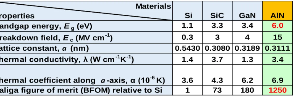
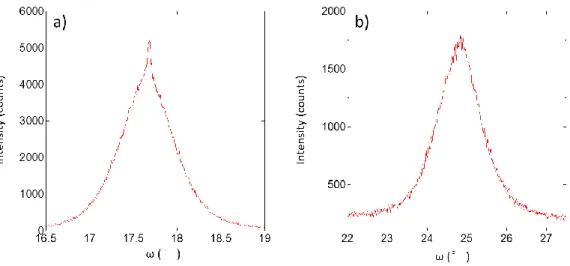
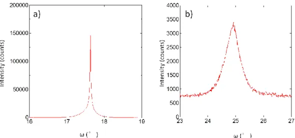
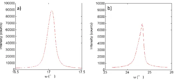
Figures 16-20 show the AlN (0002) and (10-12) XRC of AlN films sputtered at oxygen partial pressures of 5.0×10⁻¹⁰ - 9.4×10³ Pa. The shape of AlN (0002) XRC AlN films sputtered at 5.0×10⁻¹⁰, 5.5×10⁻³, and 5.6×10² Pa contained narrow and broad peaks. It indicates that the AlN films had 2 domains peak that have different tilted AlN normal to its surface (AlN c-axis direction). However, the evidence still remains not clear.
Fig. 12 AlN a) (0002) and b) (10-12) XRC profiles of AlN layer sputtered at oxygen partial pressures of 5.0×10⁻¹⁰ Pa.
Fig. 13
AlN a) (0002) and b) (10-12) XRC profiles of AlN layer sputtered at oxygen partial pressures of 5.5×10⁻³ Pa.
Fig. 14 AlN a) (0002) and b) (10-12) XRC profiles of AlN layer sputtered at oxygen partial pressures of 5.0×100 Pa.
Fig. 15 AlN a) (0002) and b) (10-12) XRC profiles of AlN layer sputtered at oxygen partial pressures of 5.6×10² Pa.
Fig. 16 AlN a) (0002) and b) (10-12) XRC profiles of AlN layer sputtered at oxygen partial pressures of 9.4×10³ Pa.
2.4.1.8 Cyrstalline quality of AlN
The dependence of AlN (0002) and (10-12) XRC-FWHM of sputtered AlN films on oxygen partial pressure is shown in Fig. 21. The (0002) and (10-12) XRC-FWHM values of AlN films sputtered at 5.0×10⁻¹⁰ - 5.0×100 Pa were decrease with increase the oxygen partial pressure. However, the (0002) and (10-12) XRC-FWHM values of AlN film sputtered at 5.6×10⁻² Pa was higher than those of AlN film sputtered at 5.0×100 Pa. Moreover, the (0002) and (10-12) XRC-FWHM values of AlN film sputtered at 9.4×10⁻³ Pa was the lowest. The AlN film
sputtered at highest oxygen partial pressure of 9.4×10³ Pa gave the best crystal quality with 486 and 1055 arcsec for AlN (0002) and (10–12) XRC-FWHM, respectively. However, these values were still larger than AlN (0002) and (10–10) XRC-FWHM of the AlN layer formed by nitridation. This value is smaller than the value of AlN films sputtered on nitrided a-plane sapphire at 800 W, 823 K, PO2 at 5.0×10⁻¹⁰ Pa (Ptotal of 105 Pa) and Ptotal of 0.4-0.6 Pa by pulsed
DC reactive magnetron sputtering in the previous paper2.20. Thus, the crystalline quality of sputtered AlN films was improved by deposition at the highest oxygen partial pressures of 9.4×10³ Pa.
Fig. 17 AlN (0002) and (10–12) XRC-FWHM values of sputtered AlN films deposited at various
oxygen partial pressures. Grey area show the AlN (0002) and (10–10) XRC-FWHM of the nitrided a-plane sapphire.
2.4.1.9 Dislocation in AlN
The dislocation density was estimated from XRD Measurement using the following formula2.21:
𝑁S = 𝛽𝑠2
4.35|𝐛𝐬|2 , 𝑁E =
𝛽𝐸2
4.35|𝐛𝐄|2 (4)
where βS and βE are the XRC-FWHM value of (0002) AlN and (10-10) AlN in radiance2.22, bs
and bE are Burger vector of screw dislocation bs = <0001> and edge dislocation bE = 1 3
<11-20>, |bS| and |bE| are the lengths of the Burgers vector of the screw component |bS|= 0.49792
nm and edge component |bE| = 0.31114 nm2.21. However, to estimate edge dislocation using
XRC-FWHM value of twist (10-10), it can be estimated from XRC FWHM value of (10-12) using following formula2.23:
𝛽(10–12)2 = 𝛽𝑠2+ 𝛽
𝐸2 (5)
where β(10-12) is the XRC-FWHM value of (10-12) of AlN. The estimated screw and edge type
dislocations of AlN film sputtered at various oxygen partial pressure were summarized in Table 2.
Table 2 Estimated screw and edge dislocation densities in AlN films sputtered at various oxygen partial pressure.
Oxygen Screw Edge partial dislocation dislocation Pressure (Pa) (a-type) (cm -2) (c-type) (cm-2) 5.0×10⁻¹⁰ 1.7×10¹⁰ 1.2×10¹¹ 5.5×10⁻³ 1.6×10⁹ 8.1×10¹⁰ 5.0×100 2.9×10⁷ 2.4×10¹⁰ 5.6×10² 1.6×10⁹ 4.5×10¹⁰ 9.4×10³ 5.2×10⁸ 4.9×10⁹ Nitrided a-plane 4.9×10⁷ 2.0×10⁹ sapphire
The screw (a-type) and edge (c-type) dislocations of AlN film sputtered at lowest oxygen partial pressure of 5.0×10⁻¹⁰ Pa were estimated to be 1.7×1010 cm-2 and 1.2×1011 cm-2, respectively. These values were 1.5 orders higher than those of AlN film sputtered at highest oxygen partial pressure of 9.4×10³ Pa (a-type = 5.2×108 cm-2 and c-type = 6.2×109 cm-2). This
result indicates that the dislocations in the AlN film sputtered at highest oxygen partial pressure of 9.4×10³ Pa was decrease by sputtering at high oxygen partial pressure owing to polarity inversion from nitrogen (-c)-polar to aluminum (+c)-polar AlN.
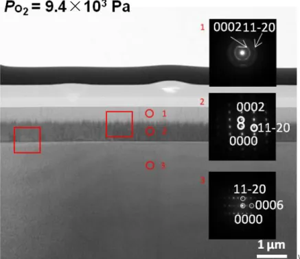
Figure 22 shows cross-sectional TEM images of AlN films sputtered at oxygen partial pressure of 5.0×100 Pa under the incident beam direction of AlN [11-20] (point 1 and 4) and AlN [1-100] (point 2, 3, and 5).
Fig. 18 Cross-sectional TEM images of an AlN layer sputtered at oxygen partial pressure of 5.0×100 Pa.
Figure 23 shows cross-sectional TEM images of AlN films sputtered at oxygen partial pressure of 9.4×10³ Pa under the the incident beam direction of AlN [1-100]. The AlN film sputtered at oxygen partial pressure of 5.0×100 Pa has two different diffraction patterns that show incident beam direction AlN [1-100] (point 2,3, and 5) and AlN [1-210] (point 1 and 4) owing to (twisted rotation of 30º) AlN while point 6 shows the diffraction pattern under the incident beam of [1-100] sapphire. The AlN film sputtered at the highest oxygen partial pressure of 9.4×10³ Pa has a ring diffraction pattern (point 1) that means polycrystalline
structure in the top part. There is a single crystal structure with an incident beam of AlN [1-100] in the bottom part, while point 3 shows the diffraction pattern of [1-[1-100] a-plane sapphire.
\
Fig. 19 Cross-sectional TEM images of an AlN layer sputtered at oxygen partial pressure of 9.4×10³ Pa.
Figure 24 shows FFT images of AlN film sputtered at oxygen partial pressure of 9.4×10³ Pa including interface of substrate and AlN film. It indicates that sputtered AlN film has 30º twist rotation to nitrided layer.
Fig. 20 FFT images of an AlN layer sputtered at oxygen partial pressure of 9.4×10³ Pa.
Figure 25 shows FFT images of AlN film sputtered at oxygen partial pressure of 9.4×10³ Pa that had 2 layers of AlN: bottom and upper part. The bottom part of AlN film was single crystal AlN and had high residual stress. On the other side, the upper part of AlN was polycrystalline AlN.
Fig. 21 FFT images of an AlN layer sputtered at oxygen partial pressure of 9.4×10³ Pa. Figure 26 shows the φ scan of AlN film sputtered at oxygen partial pressure of 5.0×100 Pa. There are 6 strong peaks and 6 weak peaks exist in the figure correspond to two different AlN domains. The φ were different 30 º each other.
Fig. 22 φ scan of AlN film sputtered at oxygen partial pressure of 5.0×100 Pa.
Figure 27 shows cross-sectional TEM images of AlN films sputtered at oxygen partial pressure of a) 5.0×100 and b) 9.4×10³ Pa. The AlN film sputtered at oxygen partial pressure of 5.0×100 Pa has many crystal defects in the whole layer along the growth direction. On the other
hand, the AlN film sputtered at highest oxygen partial pressure of 9.4×10³ Pa shows that the AlN layer is divided into two layers with a few crystal defects in the bottom layer and polycrystalline AlN in the top layer. This result is consistent with XRC-FWHM values and a few dislocation densities results.
Fig. 23 Cross-sectional TEM images of an AlN layer sputtered at oxygen partial pressure of a) 5.0×100 and b) 9.4×10³ Pa.
Fig. 28 shows cross-sectional HR-TEM images of AlN films sputtered at oxygen partial pressure of 9.4×10³ Pa which contained 2 AlN layers : upper and bottom layers in a) low and
Fig. 24 Cross-sectional TEM images of an AlN layer sputtered at oxygen partial pressure of 5×100 Pa.
Fig. 29 shows cross-sectional HR-TEM images of a) upper layer and b) lower layer of AlN film sputtered at oxygen partial pressure of 5.0×100 Pa. The upper layer has some nano grains that its boundary is shown with dominated black color. The lower layer has some curve lines that indicates that the lower layer contains residual stress.
Fig. 25 Cross-sectional HR-TEM images of an AlN layer sputtered at oxygen partial pressure of 9.4×10³ Pa
Figure 30 shows cross-sectional TEM images of AlN films sputtered at oxygen partial pressure of 9.4×10³ Pa. The This image shows small grain in the columnar structure of upper part of AlN film. The length of columnar structure is around 10 nm. Thus the upper layer has some nanograins.
Fig. 26 Cross-sectional TEM images of an AlN layer sputtered at oxygen partial pressure of 9.4×10³ Pa.
2.4.1.10 Impurity concentration in AlN
Figure 31 shows the depth profile of carbon concentration in AlN film sputtered at highest oxygen partial pressure of 9.4×10³ Pa. The oxygen concentration in AlN films sputtered at low oxygen partial pressures was estimated using O- concentration which is represented by a blue line. But in the AlN film sputtered at 9.4×10³ Pa, the O- concentration was saturated and
difficult to estimate its value. Therefore, its oxygen concentration was estimated by comparing the 18O- concentration which is represented with an orange line with that value in AlN film sputtered at oxygen partial pressure of 5.6×10² Pa.