journal or
publication title
AIMResearch - Research Highlights
volume
2013
year
2014
WPI Advanced Institute for Materials Research
The Advanced Institute for Materials Research (AIMR) at Tohoku University in Sendai,
Japan, is one of nine World Premier International Research Center Initiative (WPI)
programs established with the support of the Japanese Ministry of Education, Culture,
Sports, Science and Technology (MEXT). Since its inauguration in 2007, the AIMR has
been bringing together world-class researchers from Japan and abroad to carry out
cutting-edge research in materials science through interdisciplinary collaboration among its four
groups — Bulk Metallic Glasses, Materials Physics, Soft Materials, Device/System — and
Mathematics Unit, with further integration supported by its Interface Unit.
Led by distinguished mathematician and director Motoko Kotani, the institute promotes
interdisciplinary research across the different groups while fostering young researchers
through the Global Intellectual Incubation and Integration Laboratory (GI
3Lab), where
international joint research is carried out in close cooperation with high-profile researchers
invited from countries throughout the world.
The AIMR is host to over 140 leading researchers, around half of whom come from
abroad, including 31 principal investigators. In addition to the research hub at Tohok u
University, the AIMR collaborates with research centers in China, France, Germany, Poland,
the United Kingdom and the United States. Close ties with other leading overseas institutes
are maintained through its Adjunct Professor and Associate Professor programs.
AIMResearch
AIMResearch is an online and print publication that highlights the scientific achievements
and activities of the AIMR. First published in June 2009, AIMResearch selects the most
important papers from the wealth of research produced by AIMR scientists throughout
the year, distilling the essence of the achievements into timely, concise and accessible
research highlights that are easy to digest, but retain all of the impact and importance of the
original research article. Published monthly on the AIMResearch website in both English
and Japanese, AIMResearch research highlights bring the very best of AIMR research to a
global audience of specialists and nonspecialists alike. AIMResearch also publishes a range
of feature articles introducing other activities of the AIMR’s research groups. Visitors to the
website can register for monthly email alerts in either English or Japanese to keep abreast of
the latest developments and discoveries made at the AIMR.
RESEARCH HIGHLIGHTS
Graphene: Superconductivity thinned down
Supercapacitors: Better with a dash of gold
Organic spintronics: What matters in the long run
Superconductors: Riding the wave
Microscopy: Where rubber meets the probe
Glasses: From disorder to disorder
Molecular electronics: In the right place
Fuel cells: Improved cathodic catalysts
Organic electronics: It’s all in the twist
Metallic glasses: All in order
Spintronics: Current generation
Batteries: A crash course in nanofabrication
Biomaterials: Getting cells in line
Raman spectroscopy: Pairing up for mercury detection
Graphene oxide: Responding to infrared light
Spintronics: Using nature’s symmetries
Molecular magnets: Mathematical predictions
Batteries: The power of patterns
Superhard materials: Shear resolution
6
7
8
9
10
11
12
13
14
15
16
17
18
19
20
21
22
23
24
IN THE SPOTLIGHT
Comprehensive support for
world-class research
Materials and math makes green
Scaling the heights of materials
science research
No bridge too far
Reaping the rewards of
a mathematics–materials approach
Strengthening scientific exchange
and joint research
26
28
30
32
34
36
research.wpi-aimr.tohoku.ac.jp
AIMResearch is a publication of the Advanced Institute for Materials Research (AIMR), a Tohoku University institute funded by the Ministry of Education, Culture, Sports, Science and Technology of Japan.
© 2014 AIMR, Tohoku University. This publication may be reproduced in its original form for personal use only. Modification or commercial use without prior permission from the copyright holder is prohibited.
Editorial
AIMR, Tohoku University 2-1-1 Katahira, Aoba-ku, Sendai, Miyagi 980-8577, Japan
Editor-in-Chief Motoko Kotani
Managing Editor Takashi Takahashi
Editorial Assistant Tomoko Tagawa ISSN 1884-491X
As the director of the Advanced
Institute for Materials Research
(AIMR), Tohoku University, it
is my great pleasure to welcome
you to the fifth print edition
of AIMResearch: Research
Highlights. Each month, we
publish a selection of the
AIMR’s distinguished research
results on our bilingual website,
research.wpi-aimr.tohoku.ac.jp.
This publication is a collection of
the research highlights and feature
articles that appeared online
in 2013.
The AIMR was launched in 2007
as one of the inaugural research
centers under the World Premier
International Research Center
Initiative (WPI) program
initi-ated by the Japanese Ministry of
Education, Culture, Sports, Science
and Technology (MEXT). The
program aims to create globally
visible research centers within
Japan. As such, the AIMR is
foster-ing an ideal research environment
and becoming a hub that attracts
and circulates the world’s best
minds in materials science.
Another objective of the WPI
research centers is to create new
scientific fields through
interdisci-plinary fusion. At the end of 2010,
the AIMR decided to establish
mathematics–materials science
collaboration at the institutional
level, creating a new materials
science that is appropriate for the
twenty-first century.
Society currently faces serious
environmental and energy
problems. To solve these problems
efficiently, we have to design and
produce functional materials
based on theoretical prediction.
As mathematics can provide a
common language for all scientific
disciplines — and has the power
to rearrange and integrate the full
breadth of materials science —
mathematics is our focus.
We spent the two years prior
to 2013 rearranging our internal
organization accordingly. We first
established the Mathematics Unit
consisting of two mathematics
laboratories. Then, members of
the AIMR reformulated materials
research themes from a
math-ematical viewpoint and set three
Target Projects: Non-equilibrium
Materials based on Mathematical
Dynamical Systems; Topological
Functional Materials; and
Multi-scale Hierarchical Materials based
on Discrete Geometric Analysis.
In setting these projects,
we identified the need for
interpreters who can bridge the
gap between mathematics and
materials science. Consequently,
we established the Interface Unit
that consists of young theoretical
researchers in physics, chemistry
and applied mathematics. Rather
than belonging to a specific
laboratory, these independent
researchers can freely access
any materials scientists and
mathematicians at the AIMR. Our
approach because the
mathemat-ics–materials collaboration is
an ambitious challenge that is
accompanied by infinite
pos-sibilities of producing historical
breakthroughs. The challenge is
also accompanied by the prospect
of discovering problems
attrac-tive to both materials scientists
and mathematicians.
The AIMR achieved substantial
progress as a result of the
mathematics–materials science
collaboration during 2013.
For example, we successfully
characterized the atomic structure
of icosahedral clusters in bulk
metallic glasses. We also revealed
atomic-scale competition in energy
and geometry for glass formation
using computational homology, an
advanced mathematical concept
but not a tool of conventional
this collection.)
Globalization also featured as an
achievement in 2013. To strengthen
cooperation with international
satellites, AIMR Joint Research
Centers (AJCs) established
laboratories at the University of
Cambridge, United Kingdom, and
the University of California, Santa
Barbara (UCSB) in the United
States. The AJCs have clear roles in
joint research and in increasing the
AIMR’s international visibility.
In 2013, we held workshops
with UCSB in February and
the University of Cambridge in
November. The AIMR’s
interna-tional visibility will also benefit
from further reinforcement of our
Public Relations & Outreach Office.
In the seven years since its
inauguration, the AIMR has
produced promising results. This
is largely due to a strong belief in
the significance of our approach
and the fact that we are supported
by solid cooperation between
researchers and administrators. As
such, I believe that we can deliver
ground-breaking research findings
in the following years.
Motoko Kotani
Director
AIMR
The AIMR is leading the world in facilitating collaboration between materials science and mathematics. In
an environment where more than half of the researchers come from abroad, scientists at the AIMR —
young and international included — contribute to discussions and joint research projects, enabling the
AIMR to achieve world-leading research results.
AIMResearch’s website introduces cutting-edge research from the AIMR through research highlights,
spotlights, news and job vacancies. Access AIMResearch online now!
Latest research highlights
•
Superhard materials: Shear resolution
•
Molecular magnets: Mathematical predictions
•
Batteries: The power of patterns
•
Graphene oxide: Responding to infrared light
•
Spintronics: Using nature’s symmetries
ground-breaking technologies that cross the boundaries of conventional fields of study — bridging the disciplines of materials science, physics, chemistry and precision, mechanical, electronics and information engineering. The Mathematics Unit complements the AIMR’s research activities, and the Interface Unit further supports their integration.
Graphene has a well-earned reputa-tion as a ‘wonder material’. Isolareputa-tion of these one-atom-thick sheets of carbon that make up graphite — a material best known for its use in pencils — has opened an avenue for the study and uti-lization of two-dimensional materials. Bulk graphite has also attracted interest in its own right, especially for its poten-tial practical applications. In particular, the insertion of substances between its graphene layers to form ‘graphite intercalation compounds’ (GICs) has been investigated as a method for the storage of lithium atoms within bat-teries. Interestingly, some GICs can also conduct electricity without any resistance — an attractive phenomenon known as superconductivity.
Now, by trapping calcium atoms between just two layers of graphene, Katsuaki Sugawara and co-workers from the AIMR and the Department of Physics at Tohoku University have constructed a carbon-based supercon-ductor at its two-dimensional limit1 (see
image). Their ‘sandwich’ material offers the advantages of bulk graphite while being as thin as it can possibly be. With the production of this graphene–calci-um material, the researchers have con-structed the thinnest possible form of the calcium-based GIC C6Ca.
Among the known superconducting GICs, C6Ca is arguably the most inter-esting as it develops superconductivity at a higher temperature than any other. Sugawara and co-workers were able to reduce the thickness of the graphite layer that surrounds the calcium atoms to the absolute minimum. The thin gra-phene–calcium–graphene material was produced by first introducing lithium
into a bilayer graphene film supported by a silicon carbide (SiC) substrate — a less challenging task than the direct in-troduction of calcium, due to the smaller size of the lithium atoms. Subsequently, they replaced the intercalated lithium atoms by depositing calcium onto the graphene–lithium–graphene intermedi-ate, followed by heating. “We had ini-tially developed this method for making millimeter-thick C6Ca, and have now improved it for use in bilayer-graphene films,” explains Sugawara.
Despite the thinness of the material they created, the scientists were able to successfully perform a number of ex-periments on it. “The most important result of our study is the characteriza-tion of the electronic structure in this
thinnest limit of a GIC,” notes Sugawara. “Our findings should form a basis for understanding superconductivity in GIC systems.” The team now hopes that the same approach will be useful for other GIC applications, including the creation of efficient microbatteries. “This research area should help to gain a fundamental understanding of the physics and chemistry relevant to state-of-the-art batteries using graphite as an electrode,” says Sugawara.
1. Kanetani, K., Sugawara, K., Sato, T., Shimizu, R., Iwaya, K., Hitosugi, T. & Takahashi, T. Ca inter-calated bilayer graphene as a thinnest limit of superconducting C6Ca. Proceedings of
the National Academy of Sciences USA
109, 19610–19613 (2012).
Ca C
SiC substrate
Graphene
Superconductivity thinned down
Production of the thinnest possible carbon-based superconductor could herald
functionalized graphene materials
Schematic view of the calcium-based graphite intercalation compound (GIC) C6Ca. Calcium atoms (Ca, in
yellow) are inserted between two sheets of graphene, which are made of carbon atoms (C, in gray). The graphene–calcium sandwich is supported by a silicon carbide (SiC) substrate.
Repr oduc ed fr om R ef . 1 © 2012 K . K anetani et al .
Supercapacitors aim to surpass batteries by combining immense energy storage with lightening-quick charge times. Manganese oxide (MnO2) is a promis-ing material for these devices because of its low cost, nontoxic properties and ultrahigh capacitance. However, the compound’s intrinsically low conductiv-ity renders electron transport difficult. So far, only nanometer-thin films or low-density nanoparticle dispersions of MnO2 have displayed the desirable supercapacitance, but unfortunately these structures are too small to deliver adequate power for most applications.
Mingwei Chen, Jianli Kang and colleagues from the AIMR at Tohoku University have now devised a strategy to boost the conductivity of MnO2 thick films by fashioning them into uncon-ventional nanoporous electrodes that incorporate gold atoms within their oxide lattice1. First, the team synthesized a
po-rous MnO2 electrode by electrochemically depositing a nanoscale film with needle-like arrangements onto a gold–polymer substrate. Despite the structure providing plenty of surface sites for energy stor-age, the electrode’s capacitance dropped dramatically when the film’s thickness ex-ceeded 350 nanometers, owing to MnO2’s poor conductivity.
The researchers then bombarded the MnO2 electrode with gold atoms from a physical vapor deposition system, using a process known as sputtering. Repeating the sequence of MnO2 electrochemi-cal growth followed by gold ‘doping’ several times enabled the construction of micrometer-thick electrodes ready for use as supercapacitors. X-ray and electron microscopy analysis revealed that this technique replaces 10% of the MnO2 with
electron-rich gold dopant atoms that are distributed evenly throughout the oxide (see image). Alternate layering of MnO2 and gold atoms ensures the dopants are well-integrated within the oxide’s lattice and not just physically absorbed, Chen notes. “The electrochemical deposi-tion helps sputtered gold travel to the electrode/electrolyte interface to occupy MnO2 lattice sites.”
The gold-doped MnO2 was found to have a capacitance 65% higher than that of comparable pure films — the best charge storage ever achieved from thick MnO2 electrodes. The new material showed outstanding stability and even increased its charge capacity after a few hours’ use due to electrochemical dop-ant redistribution during voltammetric cycling. Collaboration with Kazuto Akagi’s research team at the AIMR
uncovered a fundamental theoretical principle behind these findings: gold dopants transfer electrons to manganese and oxygen atoms equally, boosting the entire material’s conductivity.
“Manganese oxide is the most promis-ing material for electrochemical superca-pacitors,” says Chen, adding that “doping is the easiest and best way to improve its conductivity.” By implementing an often-considered but rarely realized concept, the team is confident that their doping approach will benefit future commercialization efforts of MnO2 thick-film devices.
1. Kang, J., Hirata, A., Kang, L., Zhang, X., Hou, Y., Chen, L., Li, C., Fujita, T., Akagi, K. & Chen, M. Enhanced supercapacitor performance of MnO2 by atomic doping. Angewandte Chemie
International Edition 52, 1664–1667 (2013).
Supercapacitors
Better with a dash of gold
An innovative deposition technique may help to jumpstart a new generation of
high-speed energy storage materials
View of the crystal structure of manganese oxide (MnO2) (blue and red spheres) doped with an atom of gold
(yellow sphere). New findings reveal that this kind of material is ideal for supercapacitors.
© 2013 M
ingw
An ability to control the spin of the electron would enable the design of spintronic devices that are more ef-ficient than current electronic ones. Research efforts have so far focused on solid-state inorganic materials that can be fabricated to a high purity, easily incorporated into devices and whose composition can be precisely controlled. However, organic materials also pose several advantages, including low processing costs and the opportu-nity to control their physical properties through careful chemical modification.
Since organic compounds are typically made from light elements — primarily carbon — the spin–orbit interaction, which couples the spin momentum with the angular momen-tum of the electron, is quite small. This means that the electron spin can be preserved for a long time and electrons can, in principle, travel long distances without flipping their spin. Until re-cently, the longest distances travelled at room temperature were in the few tens of nanometers and a greater distance had only been observed at a low tem-perature. Xianmin Zhang and co-work-ers have now realized devices based on an organic material in which the electrons can travel distances of up to 110 nanometers at room temperature, while preserving their spin1 (see image).
The researchers constructed their devices from films of fullerene (C60), a molecule which has low spin–orbit in-teractions as it consists solely of carbon atoms. The absence of hydrogen — com-mon in other organic materials — serves to reduce the hyperfine interactions between electron and nuclear spins that can induce spin-flipping events. Zhang
and colleagues fabricated organic spin valves, in which two ferromagnetic electrodes are placed in contact with an organic layer, and measured their magnetoresistance, which is the differ-ence in electrical resistance when the spin valve’s electrodes are magnetized in the same or opposite direction. Magnetoresistance is therefore a measure of the conservation of the electron’s spin polarization.
By studying devices composed from various thicknesses of the C60 film, the team observed a record value — of up to 110 nanometers in length — for mag-netoresistance at room temperature. Zhang explains that it may be possible to further improve on these results as,
according to theory, a spin length of over 400 nanometers can be obtained in crystalline C60 — although fabricating films of such a well-ordered material would be quite challenging.
According to Zhang, the significance of the team’s results is not limited to C60: an understanding of spin transport in these films could inspire chemists and engineers to design even more ef-ficient compounds and devices.
1. Zhang, X., Mizukami, S., Kubota, T., Ma, Q., Oogane, M., Naganuma, H., Ando, Y. & Miyazaki, T. Observation of a large spin-depen-dent transport length in organic spin valves at room temperature. Nature Communications 4, 1392 (2013).
Organic spintronics
What matters in the long run
Experiments on fullerene films show that electron spins can be preserved for long
distances in optimized organic compounds
Illustration of the fullerene films in which electrons preserve their spins over long distances. Fullerenes (blue), electrons (green spheres) and electron spins (arrows) are shown.
© 2013 M iy az ak i–M izuk ami gr oup
Understanding the origin of super-conductivity in high-temperature superconductors remains a major question in physics and is crucial for the development of superconductors that can operate at higher temperatures. However, unraveling the phenomenon is complicated by the fact that electronic properties — such as magnetism — which usually prevent superconductiv-ity, appear to play an important role in the superconducting state at such temperatures. An international team led by Takashi Takahashi and colleagues from the AIMR at Tohoku University has now shown that superconductivity may coexist with these competing states1.
Superconductivity originates from the existence of pairs of electrons that can roam a crystal without losing energy. In conventional superconductors the formation of such electron pairs is facili-tated by oscillations of the atoms in the crystal. However, in high-temperature superconductors other factors including magnetism seem to play a role, despite conventional theory determining that magnetism and superconductivity can-not coexist.
The researchers studied 1T-TaS2, a ma-terial consisting of layers of the elements tantalum (Ta) and sulfur (S), as well as its iron-doped derivatives. At lower tem-peratures the tantalum atoms in 1T-TaS2 arrange into a so-called ‘Star of David’ pattern (see image) and exhibit an insu-lating behavior in which periodic varia-tions in the density of electrons — known as charge-density waves (CDWs) — arise across the material. Typically, super-conductivity and the CDW state are considered to be mutually exclusive. Yet the researchers found that when some of
the tantalum atoms were replaced with iron, superconductivity could occur.
Takahashi and colleagues used high-resolution angle-resolved photoemission spectroscopy (ARPES) — a technique in which light pushes electrons out of a material — to investigate 1T-TaS2. Measuring the energy and momentum of the ejected electrons provides a direct window into a material’s electronic state. The researchers identified a shallow elec-tron pocket, believed to be characteristic of superconductivity, within 1T-TaS2 in the nearly commensurate CDW (NCCDW) state — a CDW phase that forms at higher temperatures and partic-ular concentrations of iron. “The unique feature of this method is to reveal the electronic states responsible for the CDW state as well as the superconducting state.
This would not be possible with other experimental approaches,” explains team member Ran Ang.
The team was able to show that super-conductivity and the CDW state are not separated within 1T-TaS2 crystals but instead coexist, representing an intrinsic property and offering valuable insight into the origin of high-temperature su-perconductivity. In addition, the ability to control the CDW phase — by switch-ing between the material’s normal metal-lic and insulating states — has potential for application in electronic devices.
1. Ang, R., Tanaka, Y., Ieki, E., Nakayama, K., Sato, T., Li, L. J., Lu, W. J., Sun, Y. P. & Takahashi, T. Real-space coexistence of the melted Mott state and superconductivity in Fe-substituted 1T-TaS2.
Physical Review Letters 109, 176403 (2012). Ta
Superconductors
Riding the wave
The coexistence of superconductivity and a wave-like, charge-ordered phase in
iron-doped 1T-TaS
2offers a deeper understanding of high-temperature superconductivity
Tantalum (Ta) atoms organize into a ‘Star of David’ pattern in the charge-density wave (CDW) phase of 1T-TaS2.
© 2013 R
an A
Rubber is an important class of mate-rial with applications ranging from high-performance devices to the humble car tire. But characterizing the complex blend of cross-linked polymers and car-bon ‘filler’ particles that comprises rub-ber is far from straightforward. To better investigate its composition, researchers have turned to atomic force microscopy (AFM) — a technique that uses tiny, oscillating silicon probes to measure the physical properties of surfaces.
Conventional AFM instruments are unable to fully investigate the behavior of rubber because their probes cannot vibrate sufficiently fast across different frequencies. Now, Ken Nakajima and colleagues from the AIMR at Tohoku University have solved this problem with a design that uses so-called ‘piezoelectric’ crystal actuators to boost the sensors’ vibrational capabilities1. While actuators
allow the three-dimensional scanning of surfaces, they are designed for large movements, meaning that AFM instru-ments have a limited frequency range. To obviate this issue, the researchers in-serted an additional piezoelectric actua-tor — small, lightweight and with large resonant frequencies — above the AFM scanner to simultaneously oscillate the sample and probe it up to 20,000 times per second.
The team tested its design on a series of isoprene and styrene–butadiene rub-bers. First, they determined mechanical contact parameters by recording how increasing force deformed the materi-als. They then compared the amplitude and phase of AFM signals from the rubbers to those of a solid mica surface. Repeating the measurements at differ-ent frequencies generated ‘viscoelastic’
parameters that described the rubbers’ dynamic deformation.
Two-dimensional ‘maps’ of the me-chanical loss of a mixed rubber surface were created using the AFM scanning functions (see image). These revealed an ‘island’-like arrangement of nanoscale isoprene rubbery regions surrounded by a ‘sea’ of styrene–butadiene rubbery regions. Critically, the immiscible nature of the rubbers only became clear when scanning at a certain range of frequencies.
Nakajima notes that the ability to measure frequency-dependent deforma-tion can eliminate many of the time-consuming tests currently needed to characterize rubber. “In viscoelastic materials, frequency and temperature are believed to be related. Therefore, measurements with narrow frequency
ranges must be performed at multiple temperatures. Our instrument can carry out these measurements with a much wider frequency range at a fixed tem-perature,” he says.
Furthermore, explains Nakajima, the AFM measurements match many of the frequencies encountered during macro-scopic testing. Such direct comparisons of large- and nano-scale phenomena are vital to comprehend multi-component systems. “Our technique can visualize the viscoelastic nature of each compo-nent in high resolution, giving valuable feedback for future materials design.”
1. Igarashi, T., Fujinami, S., Nishi, T., Asao, N. & Nakajima, K. Nanorheological mapping of rubbers by atomic force microscopy.
Macromolecules 46, 1916–1922 (2013).
0.1μm
Microscopy
Where rubber meets the probe
A ground-breaking microscope design reveals the nanoscale mechanical properties
of rubber surfaces in unprecedented detail
An atomic force microscopy ‘map’ of the mechanical loss of a rubber surface, which reveals an ‘island–sea’ arrangement of immiscible rubbers. Such maps can be created at different frequencies to fully visualize the surface’s nanoscale features.
Repr oduc ed , with permission, fr om R ef . 1 © 2013 A meric an Chemic al S ociet y
Phase-change materials are of great importance in modern computing due to their use in rewritable optical disks and computer memory. They are par-ticularly suitable for these applications as they can be made to undergo a fast, reversible transition induced by light or electrical pulses. These transitions cause their molecular structure to change from an ordered crystal to an amorphous state resembling that of glass. Materials in these two states have vastly different physical properties, such as their ability to reflect light or conduct electricity, and this phenomenon can be used to encode the ‘on’ and ‘off’ states of digital bits.
An international team of researchers, including Jiri Orava from the AIMR at Tohoku University, has now discovered a completely new type of phase transition in which the material switches between two different amorphous states1. The
amorphous-to-amorphous transition is fundamentally different to known amorphous-to-crystalline transitions, and even to previously known amorphous–amorphous transitions, according to Orava.
The researchers studied As50Se50, which is composed of equal amounts of arsenic (As) and selenium (Se). When freshly deposited as a thin film, the material is amorphous but if heated to high temperatures and slowly cooled it becomes crystalline. However, the team discovered that when only mod-erately heated, As50Se50 transitions to a different — and stable — amorphous state. Similarly, when irradiated by laser light, the newly grown material forms another stable amorphous state. These two states can be distinguished by measuring the bonding energy between
the arsenic and selenium atoms, which provides a unique fingerprint for the atomic configuration.
Transitions between different amor-phous states are not unknown, but previously had only been observed in materials subjected to pressure. The change studied here can be induced through heating, suggesting that a fur-ther mechanism is responsible for these amorphous-to-amorphous transitions. This mechanism is of particular interest because the material can be reversibly switched between the two amorphous states through successive annealing and laser-exposure cycles. Switching is thought to occur at milli- to microsec-ond intervals.
Reversible switching between amorphous states resembles previously discovered amorphous-to-crystalline
transitions used in other applications. However, the new system offers the advantage that the switching process requires far less energy. “The changes in atomic arrangement take place with a relatively low cost of energy; no melting is required,” comments Orava. Moreover, the new switching paradigm involves far fewer atoms than switching to an ordered crystal, suggesting it could be used to cre-ate computer memory devices. Verifying the dynamics of this transition and its benefit for applications remains an aim of future research, says Orava.
1. Kalyva, M., Orava, J., Siokou, A., Pavlista, M., Wagner, T. & Yannopoulos, S. N. Reversible amorphous-to-amorphous transitions in chalcogenide films: Correlating changes in structure and optical properties. Advanced
Functional Materials 23, 2052–2059 (2012). Heat or light Arsenic (As) Selenium (Se)
Glasses
From disorder to disorder
A new type of phase transition in amorphous materials raises fundamental
questions about glasses and could lead to faster computer memory
Heating, as well as illuminating, a thin film of As50Se50 causes a reversible transition from one amorphous state
to another.
© 2013 Jiri O
rav
A fundamental discrepancy exists between the basic building blocks that underpin modern engineering and those found in natural organisms: while computers and electronic circuits are based on inorganic materials, such as silicon, biological processes revolve around organic molecules. Increasingly, researchers are striving to combine the two to fabricate com-plex artificial devices from organic molecules. Ikutaro Hamada, Masaru Tsukada and co-workers from the AIMR at Tohoku University and the University of Tokyo have now shown how the right choice of metal elec-trodes and operational conditions can enhance electronic performance1.
Molecular electronic devices are particularly interesting for a number of spintronic applications, which exploit the electron’s magnetic property, known as ‘spin’. “The realization of spintronic devices consisting of single molecules promises highly functional sensing, logic (computing) and information-storage devices,” says Hamada, a member of the research team. Until now, however, spin-based effects have not been strong enough to use in practical applications.
While the performance of a molecular electronic device would be chiefly dic-tated by the organic molecule, contact between the molecule and the adjacent metallic electrodes also plays a key role. The researchers fabricated devices fea-turing two magnetic nickel electrodes separated by only 1 nanometer — far enough apart to accommodate the fullerene (C60) molecule (see image). To create this precisely sized gap, they used an electromigration-based
process to move nickel atoms out of the electrodes, slowly closing the space between them.
The team then studied the effect of the electrodes’ electronic levels on the properties of the spintronic device by measuring the change in electrical resistance when they applied different external magnetic fields, a property known as magnetoresistance. By vary-ing the voltage applied, the researchers could tune the device to observe a change in resistance of up to –80%. Theoretical calculations revealed that hybridization at the nickel–C60 inter-face may be responsible for the obser-vation of this unusual negative value and, in addition, magnetoresistance was maximal when the applied volt-ages led to the perfect alignment of the
electron spins in the C60 molecule and the nickel electrodes.
These findings demonstrate that molecular electronic devices should be envisaged as a whole since it is crucial to realize an appropriate combination of metallic contacts and organic molecules. Hamada is confident that the team’s ap-proach is applicable to a range of related devices. “Using the theory developed in the present work, I believe that it is possi-ble to predict the properties of spintronic devices made from other molecules and electrodes.”
1. Yoshida, K., Hamada, I., Sakata, I., Umeno, A., Tsukada, M. & Hirakawa, K. Gate-tunable large negative tunnel magnetoresistance in Ni−C60−Ni single molecule transistors. Nano Letters 13, 481−485 (2013).
S N
N S
Molecular electronics
In the right place
Precise alignment of the electronic states in metal contacts and organic molecules is
needed to optimize performance in molecular electronic devices
An illustration of the molecular electronic device’s geometry, with a fullerene (C60) molecule (red, center) embedded within magnetic nickel electrodes. N and S represent the north and south poles, respectively, of the device’s magnetic contacts.
Repr oduc ed , with permission, fr om R ef . 1 © 2013 A meric an Chemic al S ociet y
The development of cheap and efficient fuel cells — devices that convert chemi-cal energy into electricity — is a key component of the push toward cleaner energy sources. Instead of burning fuel to produce heat, fuel cells extract energy as electrons, which can then be fed into an electrical circuit. In the most basic example — the proton exchange mem-brane fuel cell (PEMFC) — hydrogen gas is oxidized to protons and electrons at one electrode. These electrons then pass to the other electrode, via an electrical circuit, where they reduce oxygen. Lastly, the resulting oxide anions combine with the protons, which have moved through a membrane, to form water — complet-ing the same conversion as occurs when hydrogen is burnt as a fuel.
Although commercially available fuel cell systems use platinum absorbed onto carbon to catalyze the oxygen reduction reaction (ORR), the rate of the reaction is still low, meaning that a large amount of expensive and scarce platinum is required to achieve an effi-cient reaction. Now, Mingwei Chen and Xingbo Ge from the AIMR at Tohoku University and co-workers have created a cheap and active ORR platinum–cop-per catalyst1. Their system consists of
a nanoporous platinum–copper alloy core covered by a thin skin of pure platinum (see image).
Previous research revealed that the precise ratio of platinum to copper in the core of these nanoparticulate catalysts is particularly important for their function. “Controlling the com-position of bimetallic particles at the nanoscale is extremely difficult,” says Chen. “Our electrochemical dealloying can selectively dissolve the copper from
an alloy and is much easier to control.” The dealloying process itself is governed by the voltage that is applied, allowing the final composition of the catalyst to be tuned and, in turn, the optimum catalyst to be identified.
Chen and his co-workers showed that while the catalytic activity of their material can be attributed to the thin layer of pure platinum at its surface, this property can be honed by changing the composition of the catalyst’s alloy core. This is due to the way in which the atoms in the thin layer of platinum bind to the core. Correspondingly, by adjusting the platinum–copper ratio of the core, the
team was able to produce a nanoporous material that outperforms commercial platinum on carbon catalysts.
“We are now using our dealloying method to prepare other bimetallic catalysts for energy-related applica-tions,” says Chen. “In addition, we are planning industrial collaborations to promote the practical applications of these catalysts.”
1. Ge, X., Chen, L., Kang, J., Fujita T., Hirata, A., Zhang, W., Jiang, J. & Chen, M. A core-shell nano-porous Pt–Cu catalyst with tunable composition and high catalytic activity. Advanced Functional
Materials 23, 4156-4162 (2013). H2O
O2
Fuel cells
Improved cathodic catalysts
An electrochemical dealloying method allows the preparation of highly active and
tunable platinum–copper catalysts for the oxygen reduction reaction
An illustration of the nanoporous platinum–copper catalyst developed for use in the oxygen reduction reaction of fuel cells.
© 2013 M
ingw
Organic light-emitting field-effect tran-sistors (OLETs) are innovative devices that combine brilliant light production with fast electronic switching. With the potential for application in flexible low-cost displays and all-organic lasers, OLET development has so far been ham-pered by a fundamental materials-based challenge: the molecular interactions that boost the mobility of charge car-riers — a key transistor parameter — generally stifle light emission. In joint experimental1 and theoretical2 studies,
a multidisciplinary research team led by Tienan Jin, Susumu Ikeda, Hiroyuki Tamura and Katsumi Tanigaki from the AIMR at Tohoku University has found a way to preserve electron mobility and generate higher luminescence efficiency in OLETs using short chains of oxygen-ated aromatic molecules that form un-usual bent structures in the crystal state. Previously, the researchers synthesized a promising organic semiconductor known as BP2T by linking phenyl rings and thiophene — a pentagonal aromatic molecule containing a sulfur atom — into chains called oligomers. But despite BP2T’s impressive bipolar amplification characteristics, it only converted 38% of incoming photons into luminescent emissions — a quantum yield too low for OLET applications.
The team hypothesized that substi-tuting thiophene’s sulfur atom with oxygen, which turns the molecule into a furan ring, might enhance BP2T’s performance. As oxygen atoms are smaller than sulfur, this change should favor the growth of more tightly packed crystal structures — ideal for moving charge quickly. Furthermore, notes Jin, oligomerized furans have
a strong track record of brightening luminescent materials.
When the researchers synthesized the new furan-containing compound, BPFT, and incorporated it into an OLET (see image), they saw their strategy pay off — the luminescent quantum yield jumped significantly to 51%. Next, the team used X-ray crystallography to peer into BPFT’s molecular structure. Instead of being packed flatly like most aromatic molecules, the furan oligomers had a distinct structural kink resulting in alter-nation between flat and bent alignments in the solid state.
Theoretical simulations revealed that BPFT’s bending critically enhanced the OLET’s photoluminescence. According to Tamura, this particular packing arrangement ‘breaks’ the equilib-rium inherent to aromatic solids, causing asymmetric electronic dipoles to form during the transition to a photo-excited state. These dipoles then generate lumi-nescent emissions that are forbidden in totally symmetric complexes.
The researchers note that high-per-formance OLETs are rarely discovered
because diverse expertise is required to synthesize, fabricate and model organic semiconductor devices. Collaboration between different research groups proved crucial to identifying and tai-loring the BPFT structure, they add. “These results could not have been accomplished without long-term dis-cussion and complete fusion within our team,” say Jin and Tamura.
1. Oniwa, K., Kanagasekaran, T., Jin, T., Akhtaruzza-man, Md., Yamamoto, Y., Tamura, H., Hamada, I., Shimotani, H., Asao, N., Ikeda, S. & Tanigaki, K. Single crystal biphenyl end-capped furan-incorporated oligomers: Influence of unusual packing structure on carrier mobility and luminescence. Journal of Materials Chemistry C 1, 4163–4170 (2013).
2. Tamura, H., Hamada, I., Shang, H., Oniwa, K., Akhtaruzzaman, Md., Jin, T., Asao, N., Yamamoto, Y., Kanagasekaran, T., Shimotani, H. et al. Theoretical analysis on the optoelectronic properties of single crystals of thiophene-furan-phenylene co-oligomers: efficient photoluminescence due to molecular bending. The Journal of Physical Chemistry C 117, 8072–8078 (2013).
Organic electronics
It
’
s all in the twist
A small molecular bending effect helps flexible light-emitting transistors to
outshine other optoelectronic technologies
A new aromatic compound that packs into ‘bent’ solid-state crystals can produce fast organic transistors that emit bright luminescent light.
© 2013 T
Most of the glasses that we encounter everyday are transparent and appear to be rather ordinary. A closer look, however, reveals an intriguing composi-tion: glasses are basically frozen liquids, meaning that their atoms are randomly arranged. Researchers from the AIMR at Tohoku University and international collaborators have now shown that, surprisingly, the atoms of some glasses containing metallic components also display a local order that is based on icosahedral geometric structures1. “We
provide the first direct experimental evidence of the existence of icosahedral order in metallic glasses,” explains Mingwei Chen, who led the research team to this discovery, which confirms previous theoretical predictions.
Atoms in metals behave like perfect spheres, forming perfect crystals with atomic arrangements in the form of face-centered cubic (fcc) or body-centered cubic (bcc) structures, for example. Some metallic compounds can also form glasses when cooled fast enough after melting. Scientists were unsure as to why some metals form glasses instead of crystallizing and as-sumed that upon fast cooling, atoms in the metal are prevented from forming a crystal when they arrange into icosahe-dra. Such arrangements are similar in appearance to fcc crystal structures but importantly cannot form large-scale, periodic structures (see image).
To study the structure of metallic glasses, Chen, Akihiko Hirata and colleagues used an angstrom-beam electron diffraction technique in which a tiny beam of electrons is guided onto a sample of glass that is only a few atoms wide. As the electrons pass through the
glass, they are reflected by the atoms and subsequently hit a screen that records the pattern of their reflection. With the help of computer analysis, the positions of the atoms in the sample can be determined from these patterns.
While the researchers were able to confirm the icosahedral atomic structure of metallic glasses, they also found that the icosahedra were not per-fectly formed, as previously assumed. Interestingly, this slight distortion oc-curs in a way that makes the icosahedra appear even closer in structure to the fcc arrangement.
Beyond the discovery of local order in metallic glasses, the angstrom-beam electron diffraction technique itself is a
powerful way of studying compounds on the atomic scale, comments Chen. “We have just reached the starting point to understand the true relation-ship between structure and properties of disordered materials. We now have a reliable experimental method to directly investigate local atomic struc-ture, and in the present case to show the correlation between atomic-scale structure and glass formation, and perhaps even the structural origin of the glass transition.”
1. Hirata, A., Kang, L. J., Fujita, T., Klumov, B., Matsue, K., Kotani, M., Yavari, A. R. & Chen, M. W. Geometric frustration of icosahedron in metallic glasses. Science 341, 376–379 (2013).
Metallic glasses
All in order
The local atomic order of metallic glasses has been solved by electron-beam
imaging at the atomic scale
The assumed icosahedral local atomic structure of metallic glasses (left, blue), the face-centered cubic (fcc) structure of the corresponding metal crystal (right, red) and the actual distorted icosahedral arrangement of metallic glasses (center, yellow). The top and bottom rows show the same structures from a different angle.
© 2013 Ak
ihik
o Hir
The field of spintronics relies on ex-ploiting the spin of the electron in the same way that electronics is dependent on the electron’s charge. Spintronics holds exciting promise for the gen-eration of ever smaller devices, and an important step in their realization is the introduction of spin current to non-magnetic materials.
In solids, the spin and momentum of an electron are coupled, leading to a reciprocal conversion between charge and spin currents that can be described by a phenomenon known as the spin Hall effect. Whereas the ‘direct spin Hall effect’ converts current into an accumulation of spins, the ‘inverse spin Hall effect’ converts spin flow into charge current. Interestingly, both effects have been observed in metals and semiconductors.
The inverse spin Hall effect is often determined through the measure-ment of spin currents. Through a quantitative study, Lin Chen, Fumihiro Matsukura and Hideo Ohno from the AIMR at Tohoku University have now unambiguously shown that other — galvanomagnetic — effects must be taken into account when investigating spin currents1.
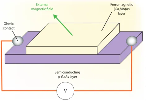
Galvanomagnetic effects are ob-served when an external magnetic field is applied to a current-carrying conductor or semiconductor material. To demonstrate their presence, Chen, Matsukura and Ohno prepared a sample comprising a ferromagnetic layer, gallium manganese arsenide ((Ga,Mn)As), on a semiconducting substrate, gallium arsenide (p-GaAs).
The researchers generated a spin cur-rent in the (Ga,Mn)As and injected it
into the p-GaAs layer using a method known as ‘spin pumping’. They then measured the resulting direct-current voltage in the p-GaAs layer. The study was carried out under ferromagnetic resonance (FMR) conditions, allowing the magnetization of the ferromagnetic layer to be characterized by FMR spec-troscopy. In particular, the team exam-ined the influences of the magnitude and angle of the external magnetic field.
Analysis of the results revealed that the expected inverse spin Hall effect was accompanied by a galvanomag-netic phenomenon — the ‘planar Hall effect’ — in the ferromagnetic (Ga,Mn)As layer. “It is especially dif-ficult to distinguish the inverse spin Hall effect from the planar Hall effect, as they both produce lines of the same
symmetry and width in FMR spectra. The difference lies in the angular dependence,” explain the researchers. “These findings indicate the critical importance of separating the origins of the direct-current voltage.”
The next step will be to show that this strategy is not just applicable to materi-als like (Ga,Mn)As that demonstrate significant galvanomagnetic effects. “This method should help further our understanding of the physics of spin current and the development of new functional spintronic devices,” says Matsukura.
1. Chen, L., Matsukura, F. & Ohno, H. Direct-current voltages in (Ga,Mn)As structures induced by fer-romagnetic resonance. Nature Communications 4, 2055 (2013).
V
Ferromagnetic (Ga,Mn)As layer Semiconducting p-GaAs layer Ohmic contact External magnetic fieldSpintronics
Current generation
A detailed, quantitative analysis of spin current reveals the importance of effects
that are often overlooked in spintronic devices
Illustration of the system devised to carry out the direct-current voltage measurements.
Repr oduc ed fr om R ef . 1 © 2013 L. Chen et al .
Developing high-capacity lithium ion batteries is an important research problem in materials science, and the realization of high-quality thin films of lithium metal oxides is a step toward this goal. Pulsed laser deposition (PLD) is a promising method of creating such films. In this tech-nique, atoms from a lithium-containing source are vaporized using high-powered bursts of light, and the resulting ‘plume’ of plasma-phase atoms subsequently lands on a designated surface as a nanometer-thin coating.
However, when depositing films of electroactive materials such as lithium, the composition of the final thin film often differs from that anticipated. This ‘non-stoichiometric’ behavior makes it hard to predict the final result of particular fabrication strategies. Although the causes of the non-stoichiometry may be attrib-uted to the volatile and chemically reac-tive nature of lithium atoms, quantitareac-tive explanations of this phenomenon have been lacking. Daniel Packwood, Susumu Shiraki and Taro Hitosugi from the AIMR at Tohoku University1 have made a
discov-ery that should significantly improve the quality of PLD lithium-based thin films thanks to a model that describes collisions between high-energy atoms during the deposition process.
During experimental trials, the re-searchers noticed that adding background pressures of oxygen gas to the PLD chamber could change the proportion of lithium in the thin film structures. Intrigued by this result, they investigated this behavior — and the role of oxygen — with a theoretical model of the scattering process as a series of two-dimensional, head-on collisions between classical par-ticles (see image).
After synthesizing several prototypical lithium–manganese oxide thin films at different oxygen pressures, Packwood, Shiraki and Hitosugi compared the films’ chemical composition to the predictions of their new model. The results were striking: the theory correctly mirrored the experimental results and revealed that the presence of oxygen gas caused lithium ions to scatter in erratic trajecto-ries, often violently. Heavier manganese atoms pushed through oxygen practi-cally unimpeded. According to the team, these findings indicate that lighter atoms will always show deficiencies when back-ground gas pressures rise above a certain threshold — thus, source materials must be chosen carefully to achieve desired lithium compositions.
Packwood notes that the model works well because it captures the physics behind the critical energy exchange oc-curring during atomic scattering. This ensures reasonable thermal equilibrium in the model and predictions of spatial distribution that have proven experimen-tally valid. The team expects that their analysis can guide the fabrication of higher-quality interfaces that would lead to lithium ion batteries with higher charge–discharge rates by reducing the effects of electrical resistance.
1. Packwood, D. M., Shiraki, S. & Hitosugi, T. Effects of atomic collisions on the stoichi-ometry of thin films prepared by pulsed laser deposition. Physical Review Letters 111, 036101 (2013).
Batteries
A crash course in nanofabrication
A collaborative study reveals that atomic collisions play critical roles during
laser-driven assembly of electroactive thin films
A representation of the combined mathematical and materials study into the deposition of electroactive thin films. The simulated trajectory of a lithium atom at an oxygen pressure of 10-6 torr (black line) is
superimposed over a plot of a lithium plasma plume after expanding for 5 microseconds at an oxygen pressure of 10-2 torr (background). Modified fr om R ef . 1 © 2013 A meric an P hysic al S ociet y
Biomaterial supports that promote the orderly growth and differentiation of cells are crucial for tissue engineering and repair. However, reproducing the structural and biological properties of the extracellular matrix, which governs cell organization in the body, remains a challenge for materials scientists. Now, Toshinori Fujie and Ali Khademhosseini from the AIMR at Tohoku University and co-workers from Japan, South Korea and the United States have devised a free-standing ultrathin polymer film that mimics the inherent ability of this matrix to direct cells. The resulting ‘nanomembrane’ exhibits nano- and microscale features, similar to those of natural tissue1.
Numerous synthetic extracellular ma-trices have previously been developed, including hydrogels and elastomers. Unfortunately, unlike their natural counterparts, the size and components of such materials hinder the hierarchi-cal assembly of cells into complex tissue structures.
Using microfabrication techniques, the researchers manufactured their film from nanometer-sized polymer fibers containing cell-adhesive domains, which allowed them to replicate the base-ment membrane of tissues — a dense, sheet-like structure that serves as a cellular scaffold.
First, they prepared an ultrathin poly-styrene film on a glass surface pre-coated with a sacrificial polymer layer. Next, using a microscopic stamp, the research-ers patterned the surface of the film with features made from a fibronectin–carbon nanotube composite to functionalize it for cell alignment and adhesion. After cell culture, they then dissolved the
initial polymer layer to release the cell-patterned nanomembrane.
In vitro cell studies showed that the
micropatterning facilitated the align-ment of muscle progenitor cells, known as myoblasts, on the nanomembrane. The fibrous nanotubes also enhanced the elongation and differentiation of these cells into functional myofibers. “These results suggest that the film’s surface is a useful platform for studying cell−sub-strate interactions,” says Fujie.
The researchers were able to produce films of various thicknesses — ranging from tens to hundreds of nanometers — by tuning the polystyrene concentration. Analyses of the thickness dependence of the mechanical properties revealed that, in addition to the free-standing films being highly flexible, the thinner films displayed greater flexibility. These unique properties allowed the team to
transform the myoblast-coated films into tubular assemblies — without damaging the cells — by rolling them around a soft silicone tube, showcas-ing the potential of usshowcas-ing the nano-membranes as scaffolds in complex tissue architectures.
The team is currently investigating how they can apply these findings to the development of flexible biodevices and tissue regeneration. “The system will be useful for mimicking blood vessels or investigating tissue responses to various drugs and toxic chemicals using lab-on-a-chip devices,” says Fujie.
1. Fujie, T., Ahadian, S., Liu, H., Chang, H., Ostrovidov, S., Wu, H., Bae, H., Nakajima, K., Kaji, H. & Khademhosseini, A. Engineered nanomembranes for directing cellular organiza-tion toward flexible biodevices. Nano Letters 13, 3185–3192 (2013).
Biomaterials
Getting cells in line
A flexible artificial extracellular matrix is paving the way for new approaches to
regenerative medicine
Differentiated muscle cells (green and blue) assembled on the ultrathin polymer film nanomembrane. The free-standing micropatterned nanomembrane is shown inset.
Repr oduc ed , with permission, fr om R ef . 1 © 2013 A meric an Chemic al S ociet y
Mercury enters drinking water from a number of sources, including the erosion of natural deposits, wastewater discharged from oil refineries and runoff from landfill and agricultural land. As its accumulation in humans can cause irreversible damage to the brain and central nervous system, the levels in water are closely monitored.
“Although many methods have been reported, developing a quantitative approach capable of detecting sub-part-per-trillion levels of mercury ions with high selectivity is still challenging,” explains Ling Zhang from the AIMR at Tohoku University. Zhang, Mingwei Chen, Qi-Kun Xue and co-workers have now designed a nanoporous gold-based optical sensor that is around 1,000 times more sensitive than conventional optical methods1. “This is the most
sensitive optical sensor for mercury ion detection in water known so far,” Xue says. “The US Environmental Protection Agency’s limit for mercury ions in drinking water is 10 nanomoles per liter, and the detection limit of our sensor is 10,000 times lower.”
The team’s sensor utilizes the tech-nique of surface-enhanced resonance Raman scattering (SERRS). Like Raman spectroscopy, SERRS relies on the fact that every molecule scatters light dif-ferently — an effect that can be weak and difficult to detect. To overcome this issue, the Raman signal is amplified in two ways. First, a roughened metal surface — in this case nanoporous gold — is used. A laser excites the gold’s surface plasmons, which increases the surrounding electric field. As Raman scattering intensities are proportional to this electric field, the signal is therefore
amplified. Second, the excitation wave-length of the laser is matched to the absorbance of the molecule being ana-lyzed. Thus, the laser light is absorbed, further amplifying the signal.
In the researchers’ study, the fluoro-chrome reporter molecule cyanine 5 (Cy5) is detected, rather than the mer-cury ion itself. Their sensor comprises flexible, single-stranded aptamers that are tagged with Cy5 and immobilized on the gold surface. Mercury ions, when present, bind to adjacent aptam-ers, pairing them to produce relatively rigid duplex-like structures (see image). This pulls the Cy5 tags up and away from the gold, resulting in a measur-able reduction in the SERRS signal.
At higher mercury concentrations, a greater number of aptamers are bound together, which further reduces the SERRS signal.
“Having successfully detected mercu-ry ions in river water and underground water,” says Chen, “we are now working on the design and fabrication of a mi-crochip that can be used in conjunction with a portable Raman spectrometer for real-world in situ detection.” The team is also looking to tweak the aptamers to test for other heavy metal ions.
1. Zhang, L., Chang, H., Hirata, A., Wu, H., Xue, Q.-K. & Chen, M. Nanoporous gold based optical sensor for sub-ppt detection of mercury ions. ACS Nano 7, 4595–4600 (2013). Cy5-labeled aptamer Nanoporous gold surface Mercury ion
Raman spectroscopy
Pairing up for mercury detection
An extremely sensitive nanoporous gold-based optical sensor improves the
detection of mercury ions in drinking water
Within the sensor, mercury ions cause aptamers to bind together in pairs, pulling the cyanine 5 (Cy5) fluorescent tags away from the gold surface and therefore changing the intensity of the Raman signal (inset graphs). Modified , with permission, fr om R ef . 1 © 2013 A meric an Chemic al S ociet y
Photodetectors, especially those that sense the infrared region of the electromagnetic spectrum, are important devices with uses in optical communication and imaging instruments. They rely on the generation of negative and positive charges — elec-trons and holes — by optical excitation. Subsequently, the charges are separated and contribute to an electrical current. However, in graphene, a material well known for its exceptional electronic properties and the foundation of several established photonics components, the electrons and holes rapidly recombine.
As a result, the amount of photocurrent that can be generated from a watt of inci-dent radiation — the photoresponse — is very low, and preparing a graphene-based photodetector has remained a challenge. Now, Haixin Chang, Hongkai Wu, Mingwei Chen and Yuichi Ikuhara from the AIMR at Tohoku University and co-workers have demonstrated the pos-sibility of enhancing the infrared photore-sponse of graphene oxide, a close relative of graphene, by controlling the structure and number of defects in the material1.
Chang’s team began by reducing few-layered graphene oxide through thermal annealing to improve its elec-tronic properties. Then, they studied the structure and type of defects found in the original and reduced graphene oxide with transmission electron microscopy and X-ray photoelectron spectroscopy. While the original material contained large do-mains of highly ordered and disordered lattices (see image), thermal annealing decreased the size of both of these areas and also affected the nature of the oxygen-containing groups.
The researchers were able to di-rectly link the structural modifications
introduced during thermal annealing to changes in the few-layered graphene oxide’s photoresponse. Under infrared illumination, the team observed a photo-current signal in the thermally annealed material that increased with the length of annealing — something they could not detect in the original.
Next, the team fabricated flexible in-frared photodetectors from the reduced few-layered graphene oxide, finding the photoresponse of the devices to be over an order of magnitude higher than that of devices made from pristine graphene. The external quantum efficiency, a mea-sure of the number of electrons and holes created by each photon under external bias, reached 97% — among the highest observed in graphene-based infrared photodetectors. Furthermore, the devices
were very stable, retaining their photores-ponse after 1,000 bending tests.
According to Chang, these findings could provide new ways to control the op-toelectronic properties of graphene-based and other two-dimensional systems. His team is currently working to improve the response time of the reduced graphene oxide, which is still quite slow. “We be-lieve that there are further opportunities to improve the photoresponse by further optimizing defects and atomic structures,” says Chang.
1. Chang, H., Sun, Z., Saito, M., Yuan, Q., Zhang, H., Li, J., Wang, Z., Fujita, T., Ding, F., Zheng, Z.
et al. Regulating infrared photoresponses in
reduced graphene oxide phototransistors by defect and atomic structure control. ACS Nano 7, 6310–6320 (2013).
Graphene oxide
Responding to infrared light
Efficient infrared photodetectors can be fabricated by controlling the atomic
structure and number of defects in graphene oxide
Transmission electron microscopy image of graphene oxide, containing large regions of high disorder (yellow line) and order (blue line).
Repr oduc ed , with permission, fr om R ef . 1 © 2013 A meric an Chemic al S ociet y
Symmetry is an important concept that must be taken into account to explain the properties of the Universe, as well as those of molecules and atomic crystals. Researchers from the AIMR at Tohoku University, together with collabora-tors from Osaka University, have now shown how the symmetry of crystals of tin telluride (SnTe) can be modified such that the material demonstrates various electronic effects1,2.
Tin telluride is a conventional semi-conductor with commercial applications in infrared photodetectors. A feature of the compound is that its crystals are mirror-symmetric, meaning that they do not change upon reflection. As a consequence, the electronic states at the surface of the crystal are protected against perturbations. Such crystals are classed as topological crystalline insula-tors and exhibit ‘topological states’ on their surface.
A practical advantage of these topo-logical states, explains Seigo Souma, a member of the research team, is that the material’s electrical conductivity is inde-pendent of size. “Normally, when we re-duce the size of the conducting material, at some point electrons cannot move and the material becomes insulating. This is a real limitation when down-sizing elec-tronic devices. However, materials with topological protection could overcome such limitations.”
In tin telluride, topological states can be controlled by changing the atomic composition of the crystal. Souma and his colleagues replaced some of the tin with lead, discovering that when the lead content was 75% or higher, the topological states disappeared1
(see image).
As well as destroying these states, the researchers also found that they could alter them. When they replaced a low percentage of the tin with indium instead of lead, the samples became superconducting at low temperatures. Owing to the symmetries of the modified crystal, the resulting material, Sn1-xInxTe, is a rare form of a topol-ogical superconductor2. Interestingly,
topological superconductors are predicted to contain an unusual class of particle known as a Majorana fermion. As their own anti-particle, these fermions possess some unique properties and are very stable to external perturbations, making them appealing for use in electronic applications.
Souma notes that with the ability to control symmetries and topological states through atomic substitution, new possibilities arise — including further investigation into the existence of the
Majorana fermion. “One interesting fu-ture possibility is to create thin layers of tin telluride/lead telluride in a device. As topological states do not only exist at the surface, but can also arise at the interface between a topological and an ordinal material, one can encapsulate the topological state between these two layers.”
1. Tanaka, Y., Sato, T., Nakayama, K., Souma, S., Takahashi, T., Ren, Z., Novak, M., Segawa, K. & Ando, Y. Tunability of the k-space location of the Dirac cones in the topological crystal-line insulator Pb1-xSnxTe. Physical Review B 87, 155105 (2013).
2. Sato, T., Tanaka, Y., Nakayama, K., Souma, S., Takahashi, T., Sasaki, S., Ren, Z., Taskin, A. A., Segawa, K. & Ando, Y. Fermiology of the strongly spin-orbit coupled supercon-ductor Sn1-xInxTe: Implications for topological superconductivity. Physical Review Letters 110, 206804 (2013).
Spintronics
Using nature’s symmetries
The different fundamental symmetries of tin telluride make it an ideal testing
ground for the study of topological states
The surface of the topological crystalline insulator tin telluride (SnTe) has electronic states (pink) that differ from those in the interior (yellow: Sn or Pb; green: Te). When the lead (Pb) content of the crystal is increased (left to right), these surface states disappear as the character of the interior becomes inverted.
Repr oduc ed fr om R ef . 1 © 2013 A meric an P hysic al S ociet y