Ph.D Thesis
Direct and indirect transitions of
angle-resolved photoemssion spectroscopy in
graphene and graphite
Department of Physics
Graduate School of Science, Tohoku University
Pourya Ayria
Acknowledgments
Since I was a child I had a dream and now I am here to fulfill my childhood dream and I am writing to tell thank you to whom help me as a human being to achieve my dream.
When I was in my country I met a researcher come from Japan in a workshop who has had an undeniable impact on my decision to come Japan. He shared a part of his life with me by telling me his life story. He was working as a cook and his mother was a Japanese dancer, one day, when he was listening to a radio program everything changed because he heard a magic sentence from the radio that was ‘if you make a decision and try to accomplish it you can change your life’. Then, he started to study physics and finally he became a physicist. I was so impressed about his story and Japan, how people can improve their life in Japan. Thus, after finishing my master, although I had a chance to continue my education in other countries I decided to go Japan.
Since I was studying during master, I read many chapters of my academic bible, ”prop-erties of carbon nanotubes” written by professors Saito, G. and M. dresslhaus and their papers about carbon nanotubes. It was my motivation to send an email to professor Saito. He replied the email and the chapter of my life in Japan started. He accepted my conditions to submit my application for the MEXT scholarship. Thanks to Japanese government that provide opportunities for students all around the world to study in Japan and have experi-ence about Japanese cultures. I participated in the entrance examination and passed it and by the support of professor Saito I could get the scholarship and join his lab. I would like to appreciate professor Saito to support me to get this position. Then, I met another Japanese person who affected on my life, professor Shinichiro Tanaka, in my first conference in Japan. He is so kind, supportive and humble person. I learned many things about ARPES from him; and, with no doubt, I can write this thesis because of the collaboration with him. I would like to appreciate professor Saito again for giving me a chance to discuss and collaborate with professor M. Dresselhaus when she came to Japan. After I met her, I understood why she is called ”Queen” not only for carbon but also as a scientist.
In Japan, my life has many ups and downs, I found two brothers, one from Indonesia, Siregar, and the other one from Brasil, Thomas. I lived with Siregar for one year and half
in the same unit of dormitory. When I was depressed and tired, he always kindly listened to me and gave me some advice. He taught me many things about Indonesia. Thomas, he is my best friend in Japan, my neighbor and collaborator. Nowadays, we are the intimate friend that sometimes we can understand each other just by looking each other. This kind of friendship will last forever. We had many discussions about group theory together. So long story short, if I want to appreciate Thomas I need to write another thesis. Thomas and Siregar emotionally supported me a lot when my father passed away and I did not have a chance to go back to my country and say my last good bye to my father who has taught not only me but also his students many lessons about the life. He taught me ‘sharing happiness brings more happiness’ and ‘nobody can build a house by destroying others house’. I would like to appreciate my mother who support me all seconds of my life, as well as my older sister who is always more worried about my life than me. I hope one day I can make up their kindness.
I would like to appreciate Dr. Nugraha, particularly for accompanying me at weekly discussion in my last semester and for helping me to write my papers. I am really thankful Hesky san to help me in my presentations. I want to say thanks to Inoue and Shirakura san for teaching me many things about Japanese culture and for doing sport together. I was very lucky to meet, Hung, he is a master of Quantum Espresso and I learned many things from him. I would like appreciate Wako san and Sato san who always helped me to fill in my documents and to do my printing job in Tohoku University. I appreciate all friends who I cannot mention their name and our stories here.
All and all some people come to our life and help us to achieve our dream and some people block it; but this is the life, and we need to ”頑張って” . I hope that all things that happened during my life in Japan will help me to become more mature, decent and knowledgeable person in my life.
Contents
1 Introduction 1
1.1 Purpose of the study . . . 1
1.2 Organization of the thesis . . . 3
1.3 General backgrounds . . . 3
1.3.1 Basics of Photoemission . . . 3
1.3.2 Angle Resolved photoemission Spectroscopy . . . 7
1.4 Photon and polarization dependence of the ARPES in graphene . . . 12
1.5 An investigation of electron-phonon coupling via phonon dispersion . . . 16
2 Basics of graphene and graphite 19 2.1 Geometrical structure . . . 19
2.2 Electronic properties . . . 22
2.3 Vibrational properties . . . 23
3 Direct and indirect transition of ARPES spectra 27 3.1 Geometry of ARPES . . . 27
3.2 Direct transition of ARPES . . . 28
3.3 Indirect transition AEPES . . . 32
3.3.1 Electron-phonon coupling . . . 34
4 Symmetry selection rules of ARPES 41 4.1 Graphene and graphite symmetry . . . 41
4.3 Indirect transition . . . 46
5 Photon energy dependent of ARPES in graphene 51 5.1 Photon and polarization energy dependence . . . 51
6 Phonon-assited indirect of ARPES in graphene and graphite 57 6.1 Phonon-assited indirect transition . . . 57
6.1.1 Resonant indirect transitions . . . 59
6.1.2 Nonresonant indirect transition . . . 62
6.1.3 Effects of s- and p-polarizations . . . . 64
7 Conclusion 65 7.1 Direct transition of ARPES spectra . . . 65
7.2 Indirect transition of ARPES spectra . . . 66
A Appendix: Electron-photon dipole vector 69 A.1 Dipole vector . . . 69
B Appendix: Fresnel equation 71 B.1 Fresnel equation . . . 71
C Appendix: Electron-phonon matrix elements 77 C.1 Atomic deformation potential . . . 77
C.2 Electron LA phonon mode coupling discussion . . . 80
D Appendix: Phonon dipersion calculation in graphene by QE 81 D.1 the self consistent calculation for graphene . . . 81
Chapter 1
Introduction
1.1
Purpose of the study
In the last decade, graphene and graphene-based atomic layer materials have provided us with intensive nanoscale research in terms of their novel electronic structures and advanced applications [1, 2, 3, 4, 5]. In order to understand various phenomena in these materials, it is necessary for us to study their electronic structure and vibrational properties of graphene based-materials. With this regard, angle-resolved photoemission spectroscopy (ARPES) is a useful method to explore electronic properties of solids. In ARPES, if the energy of photo-excited electrons surpasses the work function of the sample, the photoelectrons are ejected from the surface of a material. The kinetic energy and momentum of the photoelectron are observed by an analyzer from which we can directly get information on the electron in solids [6]. In this thesis, we will study the direct and indirect ARPES spectra near the K and Γ points, respectively, of Brillouin zone of graphene and graphite, by means of the different photon energies and light polarizations and discuss how significantly different physics from these regions are. Therefor, The purpose of this thesis, is to answer follows questions in details:
Direct transition:
1) What is the photon energy dependence of ARPES spectra in graphene? 2) What is the polarization dependence of ARPES spectra in graphene?
1) How the phonon dispersion relations of the graphene and graphite can be observed by the observation of the indirect transition ARPES spectra?
2) Which phonon mode can be observed by the ARPES? 3) What is the photon dependence of the indirect transition ? 4) What is the polarization dependence of indirect transition ?
The rest of this thesis is going to answer mentioned questions step-by-step. The study of ARPES spectra near the K point and closed to the Fermi level enable us to determine the optical properties of the the π and π∗ bands. The dependence of the ARPES intensity on the energy and polarization of an incident light play important roles to resolve the ARPES intensity because the ARPES intensity critically changes by modifying them [7, 8, 9, 10]. Changing the photon energy is assisted to determine features of the unoccupied states in graphene and graphite. The polarization of the incident light help us to analyze the symmetry selection rule for the direct and indirect transitions. Therefore, by symmetry analysis, we understand the allowed and forbidden transitions. Furthermore, the investigation of ARPES intensity from different wave vectors, particularly, around the Γ point, near to the Fermi level, in graphene and graphite, is also important because the electronic and vibrational properties in graphene and graphite can be obtained through the indirect transitions. For example, it is known that the ARPES spectra around the Γ point and near the Fermi level do not exist for the direct transition; however, there is a possibility an electrons is scattered from near the K point into near the Γ point through the indirect transition, included electron-phonon coupling and electron-photon interaction. Thus, the measurement of the energy and momentum of the scattered electron near the Γ point and near the Fermi level also provide valuable information about the electron-phonon coupling [11, 12].
In this thesis, to understand and to predict theoretically the electronic and vibrational properties of graphene and graphite by the means of ARPES technique near the K and Γ points and close to the Fermi level, we use group theory as well as computational calculation, based on first principles calculations, to explore the photon and polarization dependence of the direct and indirect transition ARPES spectra.
1.2
Organization of the thesis
The present thesis is organized as follows: In the remaining part of Chapter 1, the background for understanding the ARPES is described. In Chapter 2, the fundamentals of graphene an graphite are reviewed, particularly, regarding the geometrical structure, electronic proper-ties, and vibrational properties. The electronic structure and vibrational properties are computed by Quantum Espresso package. In Chapter 3, we show the formulation of the di-rect transition, includes the electron-photon interaction and the indidi-rect transition, includes the electron-photon interaction and the electron-phonon coupling, in ARPES. Besides, in this Chapter, we proceed the previous formulation of the electron-phonon coupling based on plane wave expansion to obtain a new (original) analytic formulation. The main (original) results of this thesis are presented in Chapter 4, 5 and 6. In Chapter 4, we will discuss about the symmetry transition rules for the direct and indirect transition in graphene and graphite[13]. In Chapter 5, we show photon energy dependence of the ARPES intensity in graphene[13]. In Chapter 6, we show how phonon-assisted indirect transition in ARPES for graphene and graphite. Finally, in Chapter 7, a summery of this thesis is given.
1.3
General backgrounds
Hereafter, in this chapter, we briefly discuss some general concepts that is important to understand ARPES as well as introduce some recent experimental results related to this thesis.
1.3.1
Basics of Photoemission
Electrons and photons are the most easily available particles with which to prob matters. Hence, many spectroscopes technique engage the use of these two types of particles [15]. In a typical spectroscopic experiment an electron or a photon in a more or less well-defined state (energy, direction of propagation, polarization) impinges on a sample. As a result the impact, electrons and/or photons escape from the sample; and, then, the escaping particles are analyzed with a spectrometer. In photoemission spectroscopy (PES), photons are incoming
Figure 1-1: In photoemission process, photons are incoming and electrons outgoing. The kinetic energy of photoelectrons are measured.
and electrons, the outgoing particles to be analyzed (see Fig. 1-1). In the most cases in solid, the photoemission process can be roughly modeled by the ”three-step model”. The three step-model is schematically shown in Fig. 1-2. In this model, it is assumed that the photoemission process can be divided into three steps:
1) The excitation of an electron by an incident photon (creation of a photoelectron), 2) Travel of the photoelectron to the sample surface,
3) Emission of the photoelectron into the vacuum by overcoming the surface potential. Then, the photoemission intensity as a function of the photoelectron kinetic energy in vacuum Ek and the excitation photon energy ℏω is proportional to the product of the
prob-abilities corresponding to each step [16]. The probprob-abilities of the three-step model are rep-resented by
P (Ek,ℏω)T (Ek,ℏω)D(Ek), (1.1)
The information on the electronic states of solids is included in the first term. In step (1), the electron is initially excited from an occupied state by the absorption of a photon into an unoccupied state. The photoexcitation probability is explained by the Fermi golden rule[17]
Figure 1-2: (a) Schematic representation of a photoemission process in the three-steps model.(b) Step (1) is the excitation of an electron by an incident photon; step (2) is travel of the photoelectron to the sample surface; step (3) is emission of the photoelectron into the vacuum by overcoming the surface potential [14].
Step (2) can be described in term of represents the probability of the photoelectron motion to the surface without serious inelastic scattering. This process can be expressed by using the absorption coefficient α(ℏω) for the incident photon and the photoelectron inelastic mean free path λmp(Ek). 1/α(ℏω) is of the order of 100–1000 ˚A or more for ℏω in the range
of 6–10000 eV which is much longer than λmp(Ek) ≤ 100 ˚A for the most element solids as
shown in Fig.1-3 [19, 18]. The T (Ek,ℏω) is given as T (Ek,ℏω) =
α(ℏω)λmp(Ek)
1 + α(ℏω)λmp(Ek)
≃ α(ℏω)λmp(Ek). (1.2)
The λmp takes a minimum of 3–5 ˚A at Ek of 15− 200 eV in many cases. This minimum
length corresponds roughly to lattice constants of various solids. Therefore, the valence-band photoemission spectra with of 15-200 eV by using a He discharge lamp or synchrotron light source mainly reflect the surface electronic states of solid. Step (3), escaping from the bulk, is the final step of the photoemission process. This process can be calculate when the photoelectrons can be treated as nearly free electrons with a potential of depth Ev−E0 ≡ V0
(this is called the inner potential), where Ev denotes the vacuum level and E0 stands for the
bottom energy in a nearly free electron band. This approximation is appropriate since the photoelectron energy is much higher than that for bound electrons in solids. In the nearly free electron model, the kinetic energy of photoelectron inside the solid is Ek+ V0 whereas it
Figure 1-3: (a) Kinetic energy dependence of the photoelectron inelastic mean free path λmp
as a function of electron energy [18]. for (a) several solids (b) 41 elements solids.
becomes Ek suddenly at the boundary. Since the ”force” is applied to the photoelectron only
perpendicular to the surface, the photoelectron momentum parallel to the sample surface is conserved on the emission into vacuum, which is one of the fundamental principle for ARPES. To satisfy the condition that the perpendicular momentum component of the photoelectron emitted into the vacuum to be possible, D(Ek) is calculated [16] as
D(Ek) = 1 2 ( 1− √ V0 Ek+ V0 ) . (1.3)
This function depends gently on Ek, and can be regarded as a constant when the recorded
kinetic energy range is narrow enough compared with Ek. Therefore, it is hereafter assumed
that the Ekdependence on the terms T (Ek,ℏω) and Dk(Ek) is negligible within the discussed
kinetic energy rage of one spectrum.
Then, electrons that overcome a solid potential, or work function, ϕ can escape from surface. The work function is define the difference between the material’s Fermi level, and the energy level of the vacuum. Fig. 1-4 shows schematically how the energy-level diagram and the energy distribution of photoemitted electrons related to each other. The solid sample has core levels and a valence band. In the the present case of a metal, the Fermi energy
Figure 1-4: The electron energy distribution, N (E), are produced for valence band or core levels by the incoming photons and measured as a function of kinetic energy Ekinis expressed
in terms of the binding energy Eb, work function ϕ and photon energy ℏω. The natural
abscissa for the photoelectrons is the kinetic energy with its zero at the vacuum level of the sample (Ek=ℏω − |Eb| − ϕ) [14].
Ef is at the top of the valence band and has a separation ϕ from the vacuum level Ev [14].
Thus, the kinetic energy of the photoelectron in vacuum can be written as
Ek =ℏω − |Eb| − ϕ, (1.4)
where, Eb, is the so-called binding energy if electrons, which in solids is generally referred
to the Fermi level and in free atoms or molecules to the vacuum level. The work function
ϕ has a substantial effect on the energy of observed electrons; but, it is common to omit it
when reporting photoemission result.
1.3.2
Angle Resolved photoemission Spectroscopy
Angle resolved photoemission spectroscopy is a kind of photoemission spectroscopy. The PES measures only the energy of electrons. ARPES measures not only the energy of electrons, but also their momentum. In this way, ARPES is a direct method to observe the band structure of solids experimentally. Figure 1-5 shows ARPES intensity as function of the
Figure 1-5: The ARPES intensity shows the electron dispersion of graphene along high symmetry point of graphene for ℏω = 100 eV [3].
binding energy along the high symmetry point of graphene for the ℏω = 100 eV. The π and
σ bands of graphene can be seen from this measurement.
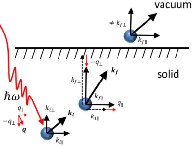
The key to understand ARPES is how the momentum of the electron in the vacuum is related to the momentum in the solid. In ARPES, the photoelectron momentum parallel to the sample surface is conserved on the emission into vacuum. As shown in Fig. 1-6, the photoelectron momentum kf is the sum of the momentum of electron in the initial state ki
and the incident photon q, in the reduce zone scheme [14], as
kf∥ = ki∥+ q∥, (1.5)
here, the photon momentum normal to the sample surface is defined as −q⊥. We can write the momentum in terms of kf and the kinetic of the energy, Ek, in vacuum
Ek =
ℏ2k2
f
2me
, (1.6)
Figure 1-6: Schematic representation of the momentum conservation at each step in the photoemission process in solids. In the figure, photon momentum normal to sample surface is defined as −q⊥ [16]. written as kf∥ ≃ 0.5˚A−1sin θ √ EV k(eV ), ∆kf∥ ≃ 0.5˚A−1cos θ √ EV k(eV )∆θ. (1.7)
The momentum resolution is obtained as
∆kf∥ = √ 2meEk 2ℏ · ∆Ek Ek sin θ + √ 2meEk ℏ cos θ· ∆θ. (1.8)
where ∆Ek denotes the energy resolution and ∆θ stands for the acceptance angle of
photo-electrons. In Eq. (1.8), the first term on the right side is negligibly smaller than the second term in general. Recently, typical ∆θ is 2◦ = 0.035 radiant or larger. If one assumes that the angular acceptance of the electron analyzer is ∆θ = 2◦ and that the detected electrons are photoexcited at the Fermi energy, one has:
∆kf∥ = 0.17˚A −1
. (1.9)
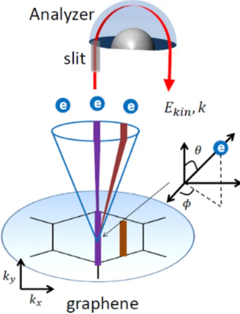
Figure 1-7: Electrons are kicked out from sample with various momentum. Only electrons exciting sample parallel to the slit (purple) will be measured. To observe a different kx, the
brown line, the sample and its corresponding emission cone are rotated until it aligns with slit [21].
a = 2.46˚A−1 is graphite lattice parameter, we can find out that the photon wave vector can be neglected. Hence, From Eq. 1.5 and Eq. 1.13
ki∥ =
√ 2mEV
k
ℏ sin θ− q∥. (1.10)
Although the momentum is not conserved along the surface normal direction, Ki⊥, it can
be obtained when photoelectrons can be treated as nearly free electrons in the solid by using the inner potential V0 and Eq. 1.5 as
ki⊥ =
√ 2mEV
k cos2θ + V0
ℏ + q⊥. (1.11)
The momentum resolution along the normal direction ∆kf⊥ is not determined from Eq. 1.11
but depends on the λmp [20, 16] as
∆kf⊥ ∼
1
(a)
(b)
(c)
(d)
Figure 1-8: (a) The photoemission intensity map of graphene is shown [3]. (b) The schematic raw data that construct the map of graphene band structure. (c) Energy density curve near the Γ point along M –Γ. (d) the momentum density from this data can be extracted.
Moreover, The two parallel components of the wave vector, shown in Fig. 1-7, can be also expressed as:
kf x= √ 2meEkV ℏ sin θ cos ϕ, kf y= √ 2meEkV ℏ sin θ sin ϕ, (1.13)
θ and ϕ are the angle describing the trajectory of the electron .
To understand how the ARPES measurement maps the electron dispersion of solid, we discuss each step of the measurement separately. Figure 1-8(a) shows the ARPES intensity as a function of the binding energy in graphene along high symmetry point. The electrons escaped from the sample it is detected in an analyzer through a slit parallel to ϕ = 0. This measurement limits the observation of the electrons with ky = 0 [21]. However, there
are possibilities that electrons with various θ, the kx spectrum, enter the analyzer. Thus,
collecting ARPES spectra from different wave vectors map the ARPES spectra which are aligns to the analyzer. For example, data collected from ARPES measurement at a given
ky maybe seen as ”slices”. The raw data for a slice is shown schematically in Fig. 1-8(b)
schematically. For a constant energy and momentum, it is referred to as energy dispersion curves (EDC) Fig. 1-8(c) or momentum dispersion curves (MDC) Fig. 1-8(d). Peaks either of these curves correspond to high photoelectron density, indicating the center of electron band. By combining a series of slices, it is possible to construct a matrix of intensity data spanning the entire Brillouin zone, which varies as a function of momentum kx and ky, and
Figure 1-9: (a) Geometry of the photoemission process [13]. The incident photon with energy ℏω are shown by an arrow going to the graphene plane. We can define a mirror plane which contains the directions of the incident light (z′ axis), the electrons ejected from the surface, and an axis (z-axis) normal to the graphene surface. The angle between incident light, the ejected electron, and the z-axis is denoted by ψ, θ. (b) Viewing the set-up from the z′ axis, the light polarization angle, ϕ, is in the x′y′-plane and measured with respect to the y′ axis. Here, ϕ = 0◦ and ϕ = 90◦ correspond to the p- and s-polarization, respectively.
binding energy Eb [21]. One common way to represent this data is as a band map. Here, an
EDC or combination of several EDC is taken for each ky. By plotting these in series, it is
possible to observe the peak shift in each on. Connecting these peak points , we are able to track the bands across key cut such as Γ− K or Γ − M in the Brillouin zone.
1.4
Photon and polarization dependence of the ARPES
in graphene
The electron energy band structure of graphene can be observed by applying different light polarizations. When the incident light polarization is parallel or perpendicular to a plane that includes the incident light and ejected photoexcited electron, they are named as p-polarized or s-p-polarized light, respectively [22] (see Fig. 1-9 (a)). Some previous studies showed that, in the ARPES spectra of graphene, π and π∗ bands near Dirac point along the
Γ –K direction are brightened by the p- and s-polarized light, respectively [7, 8, 9, 10](see
Figure 1-10: Band structure measured along Γ–K for an epitaxial graphene monolayer on SiC(0001) for two different photon energies ((a), (b): ℏω = 35 eV; (c), (d): ℏω = 35 eV ) for (a) p-polarized light (b) s-polarized light. The gray scale is linear with black (white) corresponding to high (low) photoemission intensities [10].
brightened by the s- and p-polarized light, respectively, (see Fig. 1-10 (b)). The energy band brightened by the p-polarized light is referred to as the p-branch, while that brightened by the s-polarized light is called the s-branch. Such polarization dependence is known as the electronic chirality or chiral phenomenon of graphene in ARPES spectra. Fig. 1-11 shows the corresponding Fermi surface around the K point for ℏω = 35 eV and ℏω = 52 eV with both
p- and s- polarized light. For p-polarized radiation Fig. 1-11 (a), there is no photoemission
intensity as spot 1. This situation changes drastically when using s-polarized light Fig. 1-11 (b)[10].
Some researchers in the previous studies explained the chiral phenomenon in graphene by considering the interference of electron wave functions for A and B atoms in the initial states [7, 8, 9]. They calculated the electron-photon matrix elements in the presence of p- or
s-polarized light for the ARPES intensity and they considered the wave functions of the final
Figure 1-11: Fermi surface of expitaxial graphene on SiC(0001) measured with p-polarized light ((a)-(c)) and s-polarized light ((b),(d)) for different photon energies ((a),(b): ℏω = 35 eV and (c),(d): ℏω = 52 eV) [10].
light and ejected electron. Since the dependence of the electron-photon matrix elements on the final state wave functions was not considered to explain the chiral phenomenon, they refer to the phenomenon only as the initial state effects on the electron-photon matrix elements. However, Gruneis et al. showed much earlier that, in the calculation of π − π∗ optical transition, the direction of the electron-photon dipole vectors critically depend on the final states [23]. In particular, the direction of the dipole vectors will change for different final states which are independent of light polarization. Thus, studying the final state effects on the electron-photon matrix elements is essential for ARPES spectra.
To consider the final state effects experimentally, we can apply a variation in the photon energy. Gierz et al. showed that, by applying different photon energies in ARPES measure-ment of graphene, the s-polarized light with energy of around 52 eV can illuminate both bands in the direction of Γ –K and K–M due to the change of the final states [25, 10]; their experimental measurement is shown in Fig. 1-5 (c) and (d). Therefore, the whole Fermi surface is illuminate by the s-polarized light (see Fig. 1.6 (d)).
Figure 1-12: Measured (a) and calculated (b) Fermi surface for right circular polarization light (b) left circular polarization light for different photon energies [24]. There is a discrep-ancy between experimental measurement and calculation for ℏω = 45 eV
Furthermore, they used circularly polarized light to observe polarization dependence of ARPES spectra for different photon energy [24]. Their experimental results show that the ARPES intensity for left and right circular polarization becomes almost the same near 46 eV photon energy. However, their theoretical approach did not reproduce the experimental results [24].
Motivated by the above mentioned issues, in this thesis, as the first investigation sub-ject, we combine experimental and theoretical approaches to clarify the photon energy and polarization dependence of ARPES spectra in graphene.
Figure 1-13: (a) ARPES data taken along K–M direction (solid line in the inset). (b) Dispersion (black curve) extracted by fitting the raw data. The dashed line is the fit using two straight line with different slopes. Within 20 meV below Ef, the dispersion is effect by
the resolution, and therefore, they fit the dispersion only in the range between −250 and 20 meV. The gray dotted line is a guide for the deviation of the low-energy dispersion from the extrapolation of high-energy dispersion[26].
1.5
An investigation of electron-phonon coupling via
phonon dispersion
ARPES is one of the well-established methods to probe the electron-phonon coupling (EPC) in solids [6]. The renormalization of the electronic energy and state due to the EPC have been vastly explored by the observation of the electron dispersion relation near the Dirac point (the K or K′ point) in graphene [27, 28, 29]. The EPC renormalization causes appearance of a kink structure in the electron dispersion relation. The ARPES intensity is expressed in terms of the complex self-energy where its real and imaginary parts determine the kink structure and width in the electron dispersion relation respectively [30, 31]. Fig. 1-8 shows the observation of the kink in the electron dispersion relation of graphene when ARPES data taken along K–M direction [26]. The electron dispersion of graphene as function wave vector changes linearly if the EPC is not considered; however, the EPC is renormalized electron dispersion and it causes the observation of the kink in electron dispersion.
It is known that the ARPES spectra around the Γ point and near the Fermi level (with binding energy around Eb ≈ 0–3 eV) do not exist for the direct optical transition because
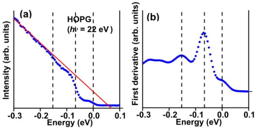
HOPG (hν = 22 eV ) -0.3 -0.2 -0.1 0.0 0.1 Intensit y (arb. units) Energy (eV) -0.3 -0.2 -0.1 0.0 0.1 First deriv ativ e (arb. units ) Energy (eV) (a) (b)
Figure 1-14: Normal-emission spectrum from HOPG showing a step-like function near 67 meV and 154 meV. (a) Integrated normal-emission spectra (b) Absolute value of the first derivative.
measurement of the ARPES intensity around the Γ point and near the Fermi level could also provide valuable information on the electron-phonon interaction [11, 12]. For example, Liu et al. have observed the ARPES spectra at the Γ point and near the Fermi level for graphene-based materials [11]. They pointed out that the observation of ARPES spectra originates from the indirect transition of electrons, which is mediated by phonons. In their experiment, the observed ARPES spectra with binding energy around 154 meV and 67 meV have been ascribed to the energy and momentum of the phonon at the K (or K′) point. They suggest that the electron is scattered from the K to the Γ point by emitting a phonon through the indirect transition. However, the phonon dispersion from their experiment could not be determined because they used photon energies of more than 20 eV.
Tanaka et al. have reported ARPES spectra of highly-oriented pyrolytic graphite (HOPG) around the Γ point and near the Fermi level for various photon energies less than 15 eV [12]. This experiment probes the energies and momenta of the electrons and phonons involved in the indirect transition, for different photon energies, so that the phonon dispersion of HOPG can be obtained (see Fig. 1-15). They found that, when the incident p-polarized photons are given to the sample surface, the ARPES intensity increases like a step-function at the binding energy around 154 meV and 67 meV for ℏω = 11.1 eV and for ℏω = 6.3 eV, respectively, and that the ARPES spectra cannot be observed for the ℏω = 13 − 15 eV in their experiment (see Fig. 1-15(b)). Then, differential of the photoelectron intensity with respect to the binding energy is calculated (see Fig. 1-15(c)). Finally, Fig. 1-15(c) and (d)
Figure 1-15: (a) Surface-normal photoelectron spectra of HOPG at 50 K taken at 6 eV ≤ ℏω ≤ 16 eV. (b) Typical spectra of HOPG taken at several photon energies along with that of the Au film at 40 K. (c) Differential of the photoelectron intensity with respect to the binding energy. (d,e) Differentials of the photoelectrons as a function of the parallel momentum of the electron.
Differentials of the photoelectrons as a function of the parallel momentum of the electron is plotted that it is express the phonon dispersion relation of the HOPG. However, not all the possible phonon dispersion relations of graphite could be well-resolved since HOPG is not a single crystal of graphite. Thus, the phonon modes involved in the indirect transition were not assigned properly from previous experimental measurements.
Therefore, the second subject of this thesis is studying the indirect transition of ARPES spectra near the Γ point and closed to the Fermi level. We will assign that which phonon modes can be involved in the indirect transition. Then, we will studying the photon and polarization dependent of the indirect transition ARPES spectra.
Chapter 2
Basics of graphene and graphite
Basic physical properties of graphene and graphite are reviewed in this section. The discus-sion includes a description of the geometrical structure, electronic properties and vibrational properties of graphene and graphite. The electronic and vibrational structures are calculated by Quantum Espresso package [32].
2.1
Geometrical structure
The electronic configuration of a free carbon atom is 1s22s22p2. When a solid is formed from carbon atoms, the electrons in the 2s and 2p orbitals form so-called hybrid orbitals that point along the chemical bonds. Depending on the crystal that we have, a different number of hybrid orbitals is required to point from two to four nearest neighbor atoms. Thus, carbon forms spn hybrid orbitals with n = 2 for graphene and graphite which are crystallized in a planar hexagonal lattice. We can define graphene as a single layer of carbon atom and it is shown in Fig. 2-1(a). Several layers of graphene sheet stacked together will form three dimensional graphite, shown in Fig. 2-1(b) and (c). The distance between planes is 0.3 nm. Bonding between layers is via weak van der Waals bonds, which allows layers of graphite to be easily separated, or to slide past each other. spn hybrid orbitals include two 2s electrons
and one 2p electron (2px or 2py in graphene plane) form three sp2 hybrid orbitals and one 2pz electron which is oriented perpendicular to the graphene plane. The 2pz electron makes a valence π band. The π band is calculated by Wannier90 package [33] and it is shown in
(a) graphene
(b) graphite
(c) graphite
(top view)
Figure 2-1: (a) Graphene is the single layer of carbon atoms hexagonal lattice. (b) Graphite has a layered, planar structure. In each layer, the carbon atoms are arranged in a hexagonal lattice. (c) Graphite (top view).
Fig. 2-2(a). The blue and red regions indicate positive and negative values of the real part of the wave function amplitudes, respectively. The in-plane sp2 make strong σ-bonds, shown in Fig. 2-2(b) .
Figure 2-3(a) and (b) shows the unit cell and Brillouin zone of graphene, respectively. The graphene sheet is generated from the dotted rhombus unit cell shown by the lattice vector a1 and a2, which are define in (x,y) coordinate as
a1 = a( √ 3 2 , 1 2, 0), a2 = a( √ 3 2 ,− 1 2, 0), a3 = c(0, 0, 1), (2.1) where the in-plane lattice parameter is a = √3aCC is the lattice constant for the graphene
sheet and aCC = 1.42 ˚A is the nearest-neighbor inter-atomic distance. The out-of-plane
lattice parameter for graphite is c = 2c0, where c0 = 3.35 ˚A, the distance between carbon
atoms on the adjacent layer planes. Thus a direct lattice vector is:
Rn = n1a1+ n2a2+ n3a3 = a (√3 2 (n1+ n2), 1 2(−n1+ n2), cn3 ) , (2.2)
where n1, n2 and n3 are integers. The unit cell consists two distinct carbon atoms from the
(a)
(b)
Figure 2-2: Surface plots for the maximally localized (a) π-band and (b) σ-bond orbital Wannier function. The blue and red regions indicate positive and negative values of the real part of the wave function amplitudes, respectively.
to the real lattice vectors a1, a2 and a3 according to the definition
ai· bj = 2πδij, (2.3)
where δij is the Kronecker delta, so that b1 and b2 are given by
b1 = 2π a ( 1 √ 3, 1, 0 ) , b2 = 2π a ( 1 √ 3,−1, 0 ) , b3 = 2π c ( 0, 0, 1 ) . (2.4)
A reciprocal lattice vector is defined
Gm = m1b1+ m2b2+ m3b3 = ( 2π √ 3a(m1+ m2), 2π a (m1− m2), 2π c m3 ) (2.5)
The first Brillouin zone of graphene is shown as a shaded hexagon in Fig. 2-3, where Γ (center), K, K′ (hexagonal corners), and M (center of edges) denote the high symmetry points.
(a)
(b)
Figure 2-3: (a) The unit cell of graphene is shown as the dotted rhombus. a1 and a2 are the
unit vectors of graphene. The graphene unit cell in real space contains two carbon atoms A and B. (b) Brillouin zone (BZ) of graphene is displayed as the shaded hexagon . The BZ is given by reciprocal lattice vectors b1 and b2 with |b1| = |b2| = √4π3a. The dots labeled
Γ, K, K′ and M in the BZ indicate the high-symmetry points.
2.2
Electronic properties
The electron dispersion relations of graphene and graphite are calculated along Γ–K–M –Γ by the quantum Espresso (QE) package [32] and it is shown in Fig. 2-4(a) and (b). Graphene has three σ bands, formed by, s, px and py orbitals, and a π band, formed by pz orbital. While, graphite has six σ bands, and two π and two π∗, bands because its unit cell has four atoms. Although the interlayer interaction is weak, this interaction has an effect on the π and
π∗ bands near the edges zone of graphite and it results in a band overlap that is responsible for the semi-metallic properties of graphite, in contrast to graphene which is a zero gap semiconductor [34]. The Brillouin zone of graphite is shown in Fig. 2-5(a). The dots labeled Γ, K, M , A, L, H in the Brillouin zone of graphite indicate the high symmetry points. Γ–A is the direction corresponding to the lattice vector normal to the surface of graphite. Fig. 2-5(b) shows the electron dispersion relation of the graphite along high symmetry points. For both graphene and graphite, we adopt the norm-conserving pseudo-potential with Perdew-Zunger (LDA) exchange-correlation scalar relativistic functional to calculate the electronic dispersion relations. The kinetic energy cut-off is taken as 60 Ry. For each atom and the kinetic energy cut-off for density potential is set 600 Ry. In order to verify the convergence of all wave functions. The k-point mesh grid for self-consistent calculation is 42× 42 × 1
(b) graphite
(a) graphene
Figure 2-4: Electron energy dispersion relation in (a) graphene, (b) graphite, calculated by QE package [32] are shown along high-symmetry points Γ–K–M –Γ.
in the graphene and 20× 20 × 4 in the graphite Brillouin zones. The lattice parameter of graphene is considered 2.4˚A and the lattice constant for unit cell normal to graphene planes
is taken as c/a = 20.0 and c/a = 2.7 for graphene and graphite, respectively.
2.3
Vibrational properties
Phonon energy dispersion relations are a fundamental physical properties of solid for deter-mining the mechanical, thermal and other condensed matter phenomena. The phonon disper-sion of graphene and graphite have been explored experimentally by inelastic neutron [35, 36], electron energy loss spectroscopy (EELS) [37, 38] and x-ray scattering [39] techniques. While, Theoretically, a number of techniques including elastic continuum model [40], force constant models [41, 42, 43], bond charge models [44] and ab-initio calculations[45, 46, 47] have been used to calculate phonon energy dispersion relations of graphene and graphite. Here, we cal-culate the phonon dispersion relations through QE package [32], which calcal-culate the phonon dispersion via Density Functional Perturbation Theory (DFPT). Thus, first, we have to find the ground state atomic and electronic configuration; then, the phonon dispersion relations are calculated by DFPT (see Appendix D). To calculate the phonon energy and eigenvec-tors of graphene and graphite, we adopted the Perdew-Burke-Ernzerhof (PBE) generalized
A L
(a)
(b)
Figure 2-5: (a) Graphite Brillouin zone showing for several high symmetry points. The dots labeled Γ, K, M , A, L, H in Brillouin zone indicate the high symmetry points. (b) The electron energy dispersion relations of graphite along the high symmetry point is calculated by QE package [32].
gradient approximation (GGA) for the exchange-correlation function. The kinetic energy cut-off is taken 100 Ry for each atom and kinetic energy cut-off for density potential is set 1200 Ry. The dynamical matrix is calculated on a 6× 6 × 1 and 6 × 6 × 3 q-points mesh in graphene [48].
The calculated phonon dispersion is shown in Fig. 2-6 for (a) graphene (b) graphite. Since there are four atoms in the unit cell of graphite, there will be twelve phonon modes. Most of the phonon modes are nearly doubly degenerate and similar to graphene [49, 50]. An exception is near the Γ point, where the acoustic modes of the single layer split in graphite into an acoustic mode (ZA) and an optical mode (ZO′), as shown in Fig. 2-6(a). In graphene, there are six phonon branches, four in-plane and two out-of-plane. At the Γ point, there are three acoustic (A) branches: (1) the transverse and (2) longitudinal in-plane acoustic phonon modes, which are labeled in Fig. 3 as TA and LA respectively, and (3) the out-of-plane acoustic phonon mode which is labeled ZA. Furthermore, there are three optical phonon modes: (1) the transverse and (2) longitudinal in-plane optical modes, which are labeled by TO and TA, respectively, and (3) the out-of-plane optical phonon mode, which is labeled by ZO. The phonon eigenvectors of graphene at the Γ point are also shown in Fig. 2-7 and each phonon mode is labeled. In graphite, the are twelve phonon modes because there
(a) graphene
(b) graphite
Figure 2-6: (a) Graphene phonon dispersion, (b) graphite phonon dispersion are calculated by QE along high-symmetry points Γ–K–M –Γ.
LA
LO
TA
TO
ZA
ZO
Figure 2-7: The vibration eigenvectors of graphene at the Γ point are shown and each phonon mode is labeled[51].
Chapter 3
Direct and indirect transition of
ARPES spectra
In this chapter, firstly, we will explain the experimental set-up of ARPES that we consider in this thesis. Then, the direct and indirect transitions mechanisms will be discussed. The direct transition, shown in Fig. 3-1(a), is a transition an electron from a valence band is excited to a conduction band by photoabsorption while the momentum of the electron does not change during this process. The direct transition is formulated by first-order perturbation theory. On the other hand, the indirect transition, shown in Fig. 3-1(b), is a transition that the momentum of the electron is also changed due to involving a photon, phonon or impurity interaction. The indirect process is formulated by second-order perturbation theory. In this thesis, we consider the indirect transition as a transition includes electron-photon interaction and electron-phonon coupling.
3.1
Geometry of ARPES
The experimental set-up of the direct transition is shown schematically [13], in Fig. 3-2(a). The graphene surface is irradiated by photons with the incident angle ψ with respect to
z axis, normal to the surface. The emitted electrons, with emission angle θ, are analyzed
with respect to their kinetic energy and momentum [22]. We can define a mirror plane which contains the incident light (−z′ axis), the electrons ejected from the surface, and
Figure 3-1: (a) The direct transition is a transition an electron from a valence band is excited to a conduction band by photoabsorption while the momentum of the electron does not change during this process. (b) the indirect transition is a transition that the momentum of the electron is also changed due to involving a photon and phonon or impurity interaction.
the axis normal to the graphene surface (z-axis). When the incident light polarization is perpendicular (parallel) to the mirror plane, the light is named s-polarized (p-polarized) light [13, 7, 8, 9]. From the z′ axis viewpoint, as shown in Fig. 3-2(b), we see that the light polarization angle can be defined by angle ϕ in the x′y′ plane and measured by the y′ axis.
ϕ = 0◦ and ϕ = 90◦ corresponds to the p and s polarization, respectively.
3.2
Direct transition of ARPES
Here, we show how to calculate the electron-photon matrix elements. The Hamiltonian for a charge particle with mass m and charge −e in an electromagnetic field with vector potential
At(t), where t index indicates the transmitted vector potential into the solid, and a periodic
crystal potential V (r) is given by
H = 1
m(−iℏ∇ + eA
Figure 3-2: (a) Geometry of the photoemission process [13]. The incident photon with energy ℏω are shown by an arrow going to the graphene plane. We can define a mirror plane which contains the directions of the incident light (z′ axis), the electrons ejected from the surface, and an axis (z-axis) normal to the graphene surface. The angle between incident light, the ejected electron, and the z-axis is denoted by ψ, θ. (b) Viewing the set-up from the z′ axis, the light polarization angle, ϕ, is in the x′y′-plane and measured with respect to the y′ axis. Here, ϕ = 0◦ and ϕ = 90◦ correspond to the p- and s-polarization, respectively.
If we neglect quadratic terms in At(t) as well as use the Coulomb gauge ∇ · At(t) = 0, the
electron-photon perturbation Hamiltonian Hopt is given
Hopt =
ieℏ
2mA
t(t)· ∇. (3.2)
The vector potential in the vacuum, Ai(t) , can be obtained from the Maxwell equation
which is given as
∇ × B = ϵ0µ0
∂E
∂t. (3.3)
The electric and magnetic fields of the incident light are
E(t) = E0exp(i(k· r + iωt)),
B(t) = B0exp(i(k· r + iωt)).
(3.4)
Hence, B =∇ × A = ik × A and B = ik × B. We can write,
∇ × B = k2A = 1
c2
∂E
Since E is a plane wave we get ∂E
∂t =−iωE then using, ω = kc, we can write Ai in vacuum
as, Ai = −iEω. Thus, the electrical field and vector potential direction are the same. The
energy density I0, of the electromagnetic wave is given by,
I0 = EB µ0 = E 2 µ0c . (3.6)
The unit of I0 is J/m2sec. Thus, the vector potential in vacuum can be written in terms of
the incident light intensity, I0 and the polarization of the electric field component P as,
Ai(t) =− i ω √ I0 cϵ0 exp(iωt)P (3.7)
where ω is the angular frequency of a photon, ε0 is the dielectric constant of the vacuum
and c is the velocity of the light.
In ARPES, we change the angle of the incident light, ψ, with respect to normal to the sample to observe different k points, (see Fig. 3-2(a)). The relationship between the angle of incident light and the transmitted light in the sample is given by Fresnel equation [52, 53, 54]. The Fresnel equation is obtained in the Appendix B. In Fresnel equation, for a given vector potential of incident light Ai in the vacuum, the vector potential of transmitted light At in
the graphene with a dielectric function ε(ω) = ε1(ω) + iε2(ω) is given as follows [52, 53, 54]:
Atx = 2 cos ψ sin ϕ
cos ψ +√ε(ω)− sin2ψ|Ai|, Aty = 2
√
ε− sin2ψ cos ψ cos ϕ
ε(ω) cos ψ +√ε(ω)− sin2ψ|Ai|, Atz = 2 cos ψ sin ψ cos ϕ
ε(ω) cos ψ +√ε(ω)− sin2ψ|Ai|,
(3.8)
where At
x,y,z are x, y, and z component of At, ϕ is the light polarization angle measured
from the y′ axis as shown in Fig. 3-2(b). In particular, ϕ = 0◦ and ϕ = 90◦ correspond to the p-polarization and s-polarization, respectively.
The electron-photon matrix element is defined by
where Ψi(k
i, r) and Ψf(kf, r) are the wave functions of an initial and a final state,
respec-tively, and k is the wave vector. When we assume that vector potential is slowly changing function of r compared with Ψi or Ψf, the electron-photon matrix element can be written
as [23]:
Mopt(ki, kf) = At(t)· D(ki, kf), (3.10)
where the dipole vector D(ki, kf) is defined as
D(ki, kf) = ⟨Ψf(kf, r)|∇|Ψi(ki, r)⟩. (3.11)
To consider the final state effects on the matrix elements, we expand the wave functions of the initial states and final states in terms of plane waves,
Ψi(ki, r) = ∑ G CGi (ki) exp ( i(ki+ G ) · r), Ψf(kf, r) = ∑ G CGf(kf) exp ( i(kf + G ) · r), (3.12)
where G are the reciprocal lattice vectors of graphene and CGi,f(k) are plane wave coefficients. We set the upper limit of photon energy as 60 eV. In this case, the optical transition occurs vertically in the k space, that is, ki ≈ kf = k. It should be noted that this assumption is
no longer valid in the XPS measurement [55]. Inserting Eq. (A.2) to Eq. (A.1), we obtain
D(k) = i∑
G
CGf∗(k)CGi (k)(k + G). (3.13)
ARPES intensity I as a function of wave vectors k and photon energyℏω can be calculated by using the Fermi’s golden role as follows [14]:
I(k,ℏω) ∝∑ i ∑ f Mopt(k) 2 δ(Ef − Ei− ℏω ) , (3.14)
where Ei and Ef are the energies of the initial and final states of the electron, respectively,
and the delta function implies an energy conservation. The absolute value is taken after the summation of the final states to assure that all interference phenomena for a given
initial state are included [56]. In our calculations, the Dirac delta function is replaced by a Lorentzian, having a finite half-width of energy 0.6 eV which is obtained by fitting to experimental spectra. The excited electrons can escape from the surface if Ef is larger than
the work function of graphene ϕwf = 4.5 eV [57].
3.3
Indirect transition AEPES
The observation of the ARPES spectra near Fermi level around Γ point can be explained by the indirect transition. Let us define the Hamiltonian Hefor electrons, Hph phonon, Hopt for
the electron-photon interaction and Hepc for the electron-phonon coupling. Then, the total
Hamiltonian is written as
H = He+ Hph+ Hopt+ Hepc, (3.15)
The unperturbed Hamiltonian of electrons and phonons is considered as H0 = He + Hph.
We adopt the adiabatic approximation which implies the total wave function can be written as a product of an electron eigenstates and phonon eigenstates[31]. Thus, the eigenstates of the unperturbed Hamiltonian are expressed as
|j⟩ = |jk⟩, (3.16) where j = i, m, f refers to an initial, an intermediate and a final state of the electron, respectively. k is an electron wave vector. The unperturbed electron and phonon dispersion relation and their eigenstates along the high symmetry points are calculated by Quantum Espresso package [32]. The calculated electron dispersions of graphene and graphite are shown in Figs. 2.4(a) and (b) and Figs. 2.5(a) and (b) , respectively.
The perturbation Hamiltonian is considered as
H′ = Hopt+ Hepc (3.17)
given by the second-order perturbation theory [58, 59]. W (kf, ki) = 2π ℏ S(kf, ki) 2δ(εi− εf). (3.18)
where εi and εf represent energy of an initial state and a final state, respectively, and S(kf, ki) is S(kf, ki) = ∑ m ⟨f|H′|m⟩⟨m, |H′|i⟩ εi − εm . (3.19)
Two processes can contribute to the indirect transition. These processes are depicted in Fig. 3-3(a). The first process is: (1) a photon excites an electron from the initial state|Aki⟩ to a state|Bkm⟩, A → B. Then, the photoexcited electron from the state |Bkm⟩ is scattered to the final state |Dkf⟩ by a phonon emission, B → D. Since the sample temperature is considered at 60 K the absorption of phonon is negligible. (2) A phonon scatters an electron from the initial state |Aki⟩ to a state |Ckm⟩, A → C. Then, a photon excites a scattered electron from the state|Ckm⟩ to the final state |Dkf⟩, C → D. These processes are expressed by the following equation:
S(kf, ki) =
⟨Dkf,|Hepc|Bkm⟩⟨Bkm|Hopt|Aki⟩
εi− εB
+ ⟨Dkf|Hopt|Ckm⟩⟨Ckm|Hepc|Aki⟩
εi− εC
,
(3.20)
The energy and momentum of the processes mentioned in Eq. (3.20) are given by
kf = ki+ q
εi− εf = Ei(ki) +ℏω − ℏωαq − Ef(kf) εi− εB = Ei(ki) +ℏω − EB(ki) εi− εC = Ei(ki)− ℏωqα− EC(kf).
(3.21)
with the wave vector q. We note since the applied photon energy is less than ℏω = 15 eV in this study, the optical transition occurs vertically [55].
In order to relate the measured energy distribution curve (EDC), namely I(E,ℏω) to the theoretical photoemission, one has to integrate over all initial states and final states. The summation on initial states and final states can perform independently when the experimen-tal conditions are chosen [14]; hence, we have
I(E,ℏω) ∝ ∑ i,f ∫ dkidkfM (kf, ki)× δ(εi− εf)δ(E− εf + ϕwf)(Nqα+ 1)f occ F , (3.22)
where ϕwf = 4.5 eV is the graphene work function [57], fFocc denotes Fermi-Dirac distribution
function of an occupied state and Nα
q is the phonon quantum number of mode α with wave
vector q. The second delta function ensures that the photoelectrons have a higher energy than the graphene work function. Therefore, in order to determine the indirect ARPES intensity, we need to calculate the electron-phonon coupling and electron-photon interaction matrix elements.
3.3.1
Electron-phonon coupling
Let us define the equilibrium position of an atom σ = A, B in the nth unit cell by Rn σ
Rnσ = Rn+ dσ (3.23)
and displacement vector of the atom by Sα
n,σ(t) and α = 1, . . . , 6 denotes the phonon modes.
The changes of the potential energy due to the lattice displacement is given by
Hepc= ∑ n,σ [Vn(r− Rnσ + S α n,σ(t))− Vn(r− R n σ)] =∑ n,σ Sn,σα (t)· ∇Rn σVn(r− R n σ). (3.24)
Figure 3-3: The electronic energy dispersion relation of graphene (b) are calculated by first-principles calculation is plotted along the high symmetry points Γ –K–M –Γ up to 15 eV. (1)A→ B → D, a photon excites an electron from the initial state |Aki⟩ to a virtual state
|Bki⟩, A → B. Then, a phonon scatters the electron from the virtual state |Bki⟩ to the final
state |Dkf⟩, B → D. (2) A → C → D, a phonon scatters an electron from the initial state
|Aki⟩ to a virtual state |Ckf⟩, A → C. Then, a photon excites an electron from the virtual
state |Ckm⟩ to the final state |Dkf⟩, C → D. The lattice displacement vector Sα
n,σ(t) is given by
Sn,σα (t) = Aαρ(q)eσα(q)eiq.Rne±iωα(q)t (3.25) where Aαρ is atomic vibration amplitude. The ± and ρ indices refer to whether a phonon is emitted (”− ” and ρ = E) or absorbed (” + ” and ρ = A). eα(q) is the unit vector of the
lattice displacement vector. ω(q) is the angular frequency of phonon with a wave vector q. The amplitude of the vibration, Aα
ρ, is given by Aαρ(q) = √ 2ℏNα ρ(q) mωα(q)N (3.26)
the number of phonons in the vibrational mode with index α given by Nα
ρ and the number
of atoms N that contribute to the phonon. m = 1.9927× 10⁻²⁶ Kg is the mass of a carbon atom.
NAα(q) = 1
exp(ℏωkα(q)
BT )− 1
We follow the rigid-ion approximation where the potential V follows rigidly the motion of the ions [31, 60]. Thus, the EPC Hamiltonian can be expressed by
Hepc =− N−1 ∑ n=0 ∑ σ=A,B 6 ∑ α=1 Aαρ(q)Sn,σα (t)· ∇rVn(r− Rn,ασ ). (3.28)
Using the perturbation theory, the non-zero matrix elements for this potential is given by
Mepcv,v′(kf, ki) =⟨kf|Hepc|ki⟩, (3.29)
where v and v′ indicate different electron bands energies. To calculate the electron-phonon matrix elements for different bands, we expand the wave function of the initial states and final states in terms of plane waves,
|kv i⟩ = 1 √ V ∑ G CGi,v(ki) exp ( i(ki+ G ) · r), |kv′ f ⟩ = 1 √ V ∑ G′ CGf,v′′(kf) exp ( i(kf + G′ ) · r), (3.30)
where V is the volume of the sample, G represents the reciprocal lattice of graphene and
CGi,f,v,v′ is the plane-wave coefficients. Thus, the electron-phonon matrix elements is given by Mepcv,v′(kf, ki) = 1 V N∑−1 n=0 6 ∑ α=1 ∑ σ=A,B ∑ G,G′ CG∗f,v′ ′(kf)CGi,v(ki) × Aα ρ(q)e iq·Rn eασ(q)· mD(kf, ki), (3.31) where mD is expressed by mD(kf, ki) = ∫ ei(kf−ki+G′−G)·r∇ rV (r− Rnσ)dr. (3.32)
We multiply the Eq. (3.31) by
thus, the electron-phonon matrix elements by changing variables r′ = r− Rn σ and dr′ = dr is given by Mepcv,v′(kf, ki) = 1 V N∑−1 n=0 6 ∑ α=1 ∑ σ=A,B ∑ G,G′ CG∗f,v′ ′(kf)CGi,v(ki) ×Aα ρ(q)e−i(kf−ki +G′−G)·Rn σeiq·Rneα σ(q)· mD(kf, ki), (3.34)
and the mD(kf, ki) is expressed by
mD(kf, ki) =
∫
ei(kf−ki+G′−G)·r′∇
r′V (r′)dr′. (3.35)
Now, the momentum conservation rule can be obtained by replacing Eq. (3.23) into Eq. (3.34) and sum over the lattice vector Rn, and using lattice point and reciprocal lattice properties that eiG·Rn = 1 N∑−1 n=0 e−i(kf−ki−q+G′−G)·Rn = δ kf,ki+q. (3.36)
Thus, the electron-phonon matrix elements become
Mepcv,v′(kf, ki) = 1 V 6 ∑ α=1 ∑ σ=A,B ∑ G,G′ CG∗f,v′ ′(kf)CGi,v(ki) ×Aα ρ(q)e−i(kf−ki +G′−G)·dσδ kf,ki+qe α σ(q)· mD(kf, ki). (3.37)
In order to proceed the calculation, we expand the ion potential of a free carbon atom, obtained by ab-initio method [61, 62, 63], into a Gaussian basis function. In the expansion of the ion potential V (r), screening from the two 1s core electrons is considered and then the fitted potential has the spherical symmetry. Since V (r) goes to minus infinity for r → 0, it is not possible to fit the potential directly. Instead we fit rV (r) and divide later by r. The potential is given by V (r) =−1 r 4 ∑ p=1 vpexp ( −r2 2τ2 p ). (3.38)
Table 3.1: The coefficient for the potential is given by substituting vp and τp into
Eq. (3.38)[61, 62, 63]. The unit of vp is [Hartree × at.u.] and τp is given [at.u.] (1 Hartree
is 27.211 eV, 1 a.u. is 0.529177) Angstrom.
p 1 2 3 4
vp -2.13 -1.00 -2.00 -0.74
τp 0.25 0.04 1.00 2.80
The fitting parameters for the potential in Eq. (3.38) is listed in table I.
Thus, by putting Eq. (3.38) into the Eq. (C.3), and considering momentum conservation
mD(kf, ki) becomes mD(kf, ki) =− i2π √ 2π Q |Q| × 4 ∑ p=1 vpτpErfi((|Q|)τp√ 2 )× exp (−((|Q|)τp√ 2 ) 2) (3.39)
where Q = q + G′− G and Erfi(z) is the imaginary error function.
Furthermore, the summation on the atomic position σ = A, B for the LO and TO branches zone center phonon q = 0 can be done analytically. Thus, when ki = kf = k
along the chosen energy counter the absolute value of the electron phonon coupling matrix elements |M(k)| are proportional to | sin θ| and | cos θ| for LO and TO modes, respectively, where tan θ = ky/kx [61].
In order to approximate the mD in two limits for long and show wave vector, we expand
exp (−z2), and Erfi(z) as follow
exp (−z2) = 1− z2+ 1 2z 4− 1 6z 6 + 1 24z 8+ .... (3.40)
It has series z → 0 given by
Erfi(z) = π−1/2(2z + 2 3z 3+1 5z + 1 21z z+ ...). (3.41)
2
4
6
8
q
0.1
0.2
0.3
0.4
0.5
0.6
ã
-q 2erfiHqL
Figure 3-4: To approximate the EPC coupling for the short and long wave phonons, we expand Erfi(q)× exp (−q2).
when z → ∞ we have Erfi(z) =−i + e z2 √ π(z −1+1 2z −3+3 4z −5+15 8 z −7+ ...). (3.42)
We plot the following function, Erfi(q)× exp (−q2), in Fig. 3-4, to approximate when the
EPC for the short and long wave phonon, q → 0 and q → ∞ respectively. Then, we can approximate the EPC for the q → 0 and q → ∞. In the case of short wave, if we assume
ωLA(q) = CLAq for LA phonon mode and expand m′D(kf, ki) for the q → 0, the expanded
EPC can be approximated by q1/2 [62]. In the case of short wave and optical phonon modes,
we can assume that the phonon frequency is almost constant ω(q) ≈ const; the expanded EPC is proportional to q−1 and finally becomes constant [64].
Chapter 4
Symmetry selection rules of ARPES
In this Chapter, we will study the selection rules in the ARPES for the direct and indirect transitions. We will introduce C2v symmetry briefly because the the experimental
measure-ments and theoretical calculation presented in this thesis is along Γ–K-M which have C2v
symmetry. Then, the selection rules for the direct and indirect transition will be obtained. Studying the selection rules in the APRES is enable us to understand when transitions is allowed and there is non-negligible ARPES spectra.
4.1
Graphene and graphite symmetry
The classification of objects according to symmetry elements corresponding to operations that leave at least one common point unchanged give rise to the point group. In graphene and graphite, the three high-symmetry points Γ, K(or K′), and M correspond to the D6h, D3h
and D2h point group symmetries, respectively. The electronic states and vibrational modes
along the K′–Γ–K and K′–M –K lines, shown in Fig. 4-1(a) with red dots line, belong to the
C2v point group, while any other general k points belong to the C1hpoint group [65, 66, 67].
The C2v point group has three kinds of symmetry operations. (1) The identity E, consists of
doing nothing: the corresponding symmetry element is an entire object. In general, object undergo this symmetry operation. (2) The 2-fold rotation about an 2-fold axis of symmetry,
C2 is a rotation through the angle 180◦. (3) The reflection in a mirror plane, σv where v

![Figure 1-3: (a) Kinetic energy dependence of the photoelectron inelastic mean free path λ mp as a function of electron energy [18]](https://thumb-ap.123doks.com/thumbv2/123deta/9881852.989864/12.918.129.800.109.433/figure-kinetic-energy-dependence-photoelectron-inelastic-function-electron.webp)
![Figure 1-5: The ARPES intensity shows the electron dispersion of graphene along high symmetry point of graphene for ℏ ω = 100 eV [3].](https://thumb-ap.123doks.com/thumbv2/123deta/9881852.989864/14.918.268.677.119.475/figure-arpes-intensity-electron-dispersion-graphene-symmetry-graphene.webp)
![Figure 1-8: (a) The photoemission intensity map of graphene is shown [3]. (b) The schematic raw data that construct the map of graphene band structure](https://thumb-ap.123doks.com/thumbv2/123deta/9881852.989864/17.918.135.817.103.294/figure-photoemission-intensity-graphene-schematic-construct-graphene-structure.webp)
![Figure 1-9: (a) Geometry of the photoemission process [13]. The incident photon with energy ℏ ω are shown by an arrow going to the graphene plane](https://thumb-ap.123doks.com/thumbv2/123deta/9881852.989864/18.918.263.684.101.373/figure-geometry-photoemission-process-incident-photon-energy-graphene.webp)

![Figure 1-12: Measured (a) and calculated (b) Fermi surface for right circular polarization light (b) left circular polarization light for different photon energies [24]](https://thumb-ap.123doks.com/thumbv2/123deta/9881852.989864/21.918.272.689.101.588/measured-calculated-circular-polarization-circular-polarization-different-energies.webp)