Design for Strong Testability of RTL Data Paths to Provide Complete Fault
Efficiency
Hiroki Wada Toshimitsu Masuzawa Kewal K. Saluja Hideo Fujiwara
Graduate School of Information Science, Nara Institute of Science and Technology
8916-5 Takayama, Ikoma, Nara 630-0101 Japan
hiroki-w masuzawa fujiwara @is.aist-nara.ac.jp
Department of Electrical & Computer Engneering, University of Wisconsin-Madison
1415 Engneering Drive, Madison, WI 53706-1691, USA
Abstract
In this paper, we propose a DFT method for RTL data paths to achieve 100% fault efficiency. The DFT method is based on hierarchical test and usage of a combinational ATPG tool. The DFT method requires lower hardware over- head and shorter test generation time than the full scan method, and also improves test application time drastically compared with the full scan method.
1. Introduction
To ensure the reliability of VLSI circuits, it is desirable to test the circuits using test patterns with high fault effi- ciency(FE)1for the entire single stack-at faults. But it is too complex to generate test patterns with high FE for a sequen- tial circuit. Thus many design-for-testability (DFT) meth- ods are proposed. A commonly used DFT method is the
”full scan”. In this approach, all latches in a gate level cir- cuit are modified into scan latches and are concatenated to a chain. Because test patterns for a scan-designed circuit can be generated by an automatic test pattern generator (ATPG) for combinational circuits, test patterns with 100% FE can be obtained. However this approach has two disadvantages: heavy hardware overhead and long test application time.
To solve these disadvantages, some DFT methods target- ing higher designs than gate level circuits are proposed. The higher design consists of two partial circuits: a controller and a data path[1]. A data path consists of three kinds of components: operational modules, registers and an inter- connecting network. Such a data path is called a register- transfer-level (RTL) data path. Because the hardware size of a data path is much larger than that of the controller, most DFT methods for higher designs target data paths.
Norwood and McCluskey[3, 4] have proposed a DFT
1Fault efficiency is the ratio of the number of faults identified as either detectable or redundant to the total number of faults.
method, the orthogonal scan, that utilizes data path flow for the scan type operation and avoids forming an explicit scan path. This method potentially reduces the hardware over- head compared with the full scan design. Test generation for a circuit designed with this approach can be carried out in the same way as the full scan : it treats the combinational logic in the complete data path as a single block. As a re- sult this method requires a substantial test generation effort. Further, this approach does not benefit from the available RTL description of the circuit and its design hierarchy.
The approaches proposed in Genesis[5, 6, 7] and H- SCAN[8] also make use of the data path flow. These ap- proaches are based on hierarchical test generation[2]. the hierarchical test generation method makes test patterns hav- ing high FE with short time as follows.
1st Step:Test patterns for every hardware element 2are generated by using the gate level circuit of .
2nd Step:A test plan for is generated by using RTL data path circuit. The test plan for is the sequence of control signals that activate the propagation of a test pattern to from a primary input of the data path and the propagation of the response to a primary output.
In those approaches test multiplexors are added in or- der to guarantee the existence of a test plan for every mod- ule. But the expected area overhead caused by the wire con- cerned with the test multiplexors can still be high. Further, the test plan generation algorithm of Genesis causes back- tracks and results in high complexity. Thus Genesis seems inefficient for large data paths. H-SCAN, like the orthogo- nal scan, relies on test generation for the complete data path as a single combinational block. Thus, H-SCAN requires substantial test generation effort and can not to make use of the design hierarchy. The DFT approach proposed by Ghosh et. al.[6, 7] incorporates RTL knowledge into test generation, but the resulting circuit often does not meet the
2Hardware element is a sub-circuit that is treated as an atomic compo- nent in RTL circuit.
13th International Conf. on VLSI Design, pp. 300-305, Jan. 2000.
100% FE goal.
We propose a DFT method for modifying a data path so that a test plan for every module can be generated with lower complexity than Genesis. The advantages of the pro- posed method are summarized as follows:
1:100% FE for the single stack-at fault set 2:Low DFT overhead
3:Short test application time
4:Use of combinational test generation 5:Hierarchical testing
2. Data Paths
The architecture of data paths treated in this paper is based on a multiplexed data path architecture[1]. This architecture has the following characters:
Every operational module can be constructed as a com- binational circuit.
Interconnecting network is made of multiplexors. We can regard such a data path as a concatenation of hard- ware elements and wires. Hardware elements consist of op- erational modules, registers, multiplexors, primary inputs and primary outputs. Values enter into a hardware element through its input ports, and exit through its output port. Each wire connects between one input port of a hardware element and one output port of another.
The following restrictions are introduced into our data path architecture in order to simplify the problems dis- cussed in section 4.
(A1) For any input port, there exists a path from a primary input. And for any output port, there exists a path to a primary output.
(A2) An operational module has only one or two input ports and only one output port.
(A3) All wires have the same bit width.
The following remedies for some substructure that vio- lates the above restrictions enable us to handle practical de- signs. The concatenation of a constant-register and an oper- ational module violates the restriction (A1). The constant- register provides a constant value to the operational module. There is no path from a primary input to the input port of the operational module connected directly to the constant- register. This substructure is regarded as an operational module having a single input port. The operational mod- ule that has more than 3 input ports violates the restriction (A2). Such a module may be regarded as a concatenation of 2 input modules.
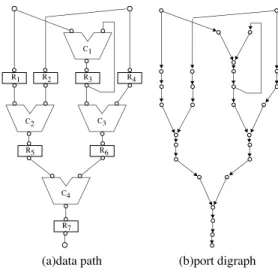
We use a port digraph to represent direct dependencies between ports: a node represents a port of the data path, and an arc implies that either a line connects to , or and are input and output ports, respectively, of the same element. Fig. 1 is the example that demonstrates the correspondence between a data path and its port digraph.
C1
C2 C3
C4
R7 R6 R5
R4 R3 R2 R1
(a)data path (b)port digraph
Figure 1. Data Path & Port Digraph
A path in a port diagraph is denoted by a sequence of ports such that there is an arc
for each . We also call and are its
start nodeand terminal node, respectively. There is natural correspondence between a path in the port digraph and a data path flow in the data path. The sequential depth of a path is the number of the registers that appear in the path.
Further, a hardware element may have a control port to feed control signals in and/or a status port to report results to the controller. In this paper, we assume that every control port is completely controllable and that every status port is completely observable.
3. Strong Testability
Hierarchical test is a promising way for testing very large sequential circuits. In the hierarchical test, testing for each hardware element proceeds as follows.
1.Test patterns are generated for (a combinational cir- cuit) using a combinational ATPG tool.
2.The test patterns are applied to : the values are fed through primary inputs at appropriate times, so that the de- sired test patterns can be applied to .
3.The responses of to the test patterns are propagated to primary outputs for observation.
A test plan specifies the control signals so that the test patterns and the responses can be propagated.
During test of a hardware element , we have to apply several test patterns to . Generally, test plan generation can be very complex due to feedback effects in a large se- quential circuit. Use of DFT can alleviate the difficulty of this problem to a certain degree. However, in this paper we study the use of DFT at RTL level in conjunction with hierarchical testing, as a result we will find the concept of strong testabilityof a data path, defined below, particularly useful.
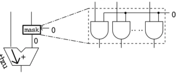
mask
+ 0 0 thru
0
Figure 2. Thru Function with Mask
Definition 1 A data path is strongly testable iff there exists a test plan for each hardware element that makes it pos- sible to apply any pattern to and to observe any response of .
A strongly testable data path has the following advan- tages.
Fast test pattern generation: Test pattern generation time is short since a combinational ATPG tool can be used. Moreover, it is shorter than that of the full scan design, be- cause the ATPG tool is applied to each hardware element separately and not to the whole circuit at once.
Fast test plan generation: Test plan generation time is short since test plans are generated at RTL (not at gate level).
100% fault efficiency: 100% fault efficiency is achieved for the whole circuit, since each hardware element is a small combinational circuit and is completely controlled and observed.
4. DFT for strong testability 4.1. Overview
In our DFT method, we add no special path for propa- gating test patterns and responses. Instead, test patterns and responses will be propagated along existing paths. Below we provide an informal and heuristic explanation for the development of the algorithm.
Consider testing of an embedded hardware element with two input ports, and , in the data path. To test , a value specified by a test pattern should be fed into input ports and . We propagate the value along a path from a primary input to . If an operational module appears in , the output value of will depend on the function of and its input value(s).
In order to guarantee that the output of is completely controllable by the input port on , thru function is added to . Most of the popular operational modules (e.g. adder) can realize the thru function by using a mask element. It generates a constant what is required to realize the thru function. Figure 2 illustrate the mask element. In our DFT process, others are so modified as to realize the thru func- tion (See Fig. 3 for example).
However, we cannot achieve the strong testability by adding only the thru functions. The thru functions guaran- tee controllability of a single path. Presence of reconvergent
th ru Op.
MUXOp.
(a)desired function (b)realization Figure 3. Thru Function without Mask paths in a data path can prevent application of a desired in- put to a two-input module. In particular, this can happen if the paths for propagating the values start from the same primary input and have the same sequential depth. Such re- convergence of paths will cause a timing conflict, i.e. two different values at a primary input at the same time. To re- solve such conflicts, in our DFT method, certain registers are augmented with hold function.
The goal of the DFT is to make a given data path strongly testable with the minimum hardware overhead. Practical implementation of the algorithms also dictates that the com- putation time for the DFT insertion and test plan genera- tion algorithms be manageable. Computation times of these algorithms we propose are and respectively, where is the number of hardware elements in a given data path3. In this section we describe the heuristic algorithm for the DFT insertion. The heuristic algorithm for the DFT insertion proceeds in three stages consisting of generation of necessary graph models (stages 1 and 2) and addition of DFT functions (stage 3).
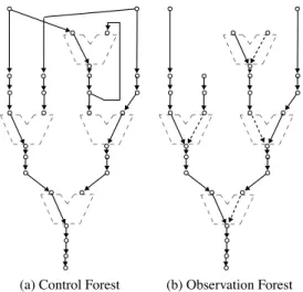
(Stage 1) Construct a control forest: To determine paths to propagate test patterns, we construct a control forest. The control forest is a spanning out-forest4of the port digraph where primary inputs are roots, and its paths are used to propagate test patterns.
(Stage 2) Construct an observation forest: To determine paths to propagate responses, we construct an observation forest. The observation forest is a spanning in-forest5of the port digraph where primary outputs are roots, and its paths are used to propagate responses.
(Stage 3) Add DFT functions: To make the data path strongly testable, we add DFT functions (thru function and hold function) to the data path at strategic locations. 4.2. Details
Control Forest(stage 1): The path used for propagating any test patterns, from a primary input to the input port of a hardware element, is called a control path to the port. On reducing the hardware overhead, the control path should be carefully chosen among all the paths from primary inputs
3The limitation of space prevents us describing the details of the test plan generation algorithm. See [9].
4A directed forest in which each port is reachable from some primary input.
5A directed forest in which there is path from each port to some primary output.
(a) Control Forest (b) Observation Forest
Figure 4. Control & Observation Forests to the port. In our method, to keep the number of added mask elements as small as possible, we choose the control paths for each port such that collection of all the chosen paths form an out-forest of the port digraph. This choice guarantees that a mask element is added to only one of the input ports of each two-input operational module. We call the resulting out-forest a control forest. Because the smaller sequential depth intuitively contributes to reduce the test ap- plication time and to relax the complication of the test plan generation, we also pay attention to the the sequential depth of the path while choosing a path. Thus, the control forest construction algorithm constructs a shortest6spanning out- forest of the port digraph. In Fig. 4 (a), we show a control forest of the data path of Fig. 1.
In the control forest obtained by the above method, for each hardware element with two input ports, one of the ports has an outgoing arc, while the other port must be a leaf (with no outgoing arc). We call the input port with an outgoing arc the first input port of , and the other port is called the second input port of .
Observation Forest(stage 2): The path used for propagat- ing the responses of a hardware element from its output port to a primary output is called an observation path of the out- put port. Since control paths, described above, have the ca- pabilities of propagating signal values, we choose an obser- vation path that is made up of minimum number of control paths. If there are several such paths, each consisting of a minimum number of control paths, then we choose a path such that the collection of all chosen paths, one for each port, forms an in-forest of the port digraph. We call the in- forest an observation forest, and the arcs that appear on the observation forest, but not in the control forest, are called junction arcs. In Fig. 4 (b), we show an observation forest
6Any path from a primary input to a port in the forest is shortest in terms of the sequential depth among all the paths from primary inputs to the port.
M y x
R PI
M v u
PI
w M'
x y
Rx Ry
M v u
PI
w R z
x y
(a) (b) (c)
Figure 5. Addition of Hold Function of the data path in Fig. 1 and the dashed lines in the figure represent the junction arcs.
As in the case of control forest, we construct the observa- tion forest by constructing a shortest7spanning in-forest of the port digraph concerned with the number of the second input ports.
DFT Functions(stage 3): The DFT functions are added as follows so that any value can be propagated along the con- trol paths and the observation paths.
Thru function: For each operational module , the thru functions are added between its input port and its output port. In the case the thru function between the second input port of and its output port is realized by using mask el- ement on its first input port, the mask element is removed because the desired constant can be provided through the control path th the first input.
Hold function: Registers are augmented with hold function to resolve timing conflicts that may arise. Below we explain how such conflicts arise and provide solution by dividing them to three cases, H1, H2 and H3.
Timing conflict can arise, while propagating test pat- terns, at the two input ports of a hardware element with control paths forming reconvergent paths and with identical sequential depth of the two ports. This situation is handled in case H1.
The timing conflicts can also arise while propagating re- sponses as follows. The propagation path consists of parts of control paths connected by junction arcs. The responses can be easily propagated along the control path parts us- ing the mask elements. However, it is more complicated to propagate the responses along a junction arc corresponding to an operational module. Let be the junction arc at an operational module , and and be the correspond- ing input and output ports. To propagate the responses along , we use the thru function between and . However,
7A path from a port to a primary output in the forest is shortest if the number of the second input ports on the path is smallest among all paths from the port to primary outputs.
Figure 6. DFT Result for Data Path in Fig. 1 since is a junction arc, is the second input port and the other input port has no mask element that feeds a con- stant o realize the thru function. Thus, such a constant is propagated from a primary input to using the control path of . This may cause a timing conflict between the control path of and a control path used for propagating either the test patterns to the module under test or a similar constant to a preceding operational module on the observation path. Since the control paths are the paths with the minimum sequential depths, such a timing conflict is caused only if . In this situation we consider a forest , obtained from the observation forest , by removing all
junction arcs such that . The
hold function addition in such a case is described in cases H2 and H3.
H1: For a port of a hardware element , let
denote the sequential depth of and denote the start node (a primary input) of the control path of . If and are the first and the second input ports of a two input
hardware element such that and
, then augment register with a hold function, where is the nearest register to in the control path of (Fig. 5 (a)).
H2: Let be any multiplexor, and and be its input ports. If satisfies the following two conditions, then reg- isters and are augmented with hold function, where (resp. ) is the nearest register to (resp. ) in the control path of (resp. ) (Fig. 5 (b)).
1. Port is reachable from in by a path of sequential depth 0, and
2. .
H3: If register satisfies the following conditions, then augment with hold function (Fig. 5 (c)). Note that (resp. ) denotes the input port (resp. the output port) of .
1. Port is reachable from in by a path of sequential depth 0, and
2. there is a port reachable to in such that
Table 1. Circuit characteristics GCD 4th IIR Paulin
#PIs 2 1 2
#POs 1 1 2
#registers 3 12 7
#MUXs 3 3 8
#op.s 5 5 7
Table 2. Test generation time (sec.)
bit- GCD 4th IIR Paulin
width ours F.S. ours F.S. ours F.S.
8 1.1 0.5 0.8 0.7 1.2 1.4
16 1.6 1.7 1.3 2.2 2.8 4.5
32 5.8 7.5 11.5 33.7 11.3 18.2
.
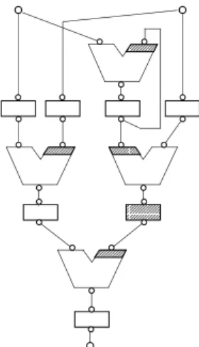
Fig. 6 shows a DFT result for the data path in Fig. 1.
5. Experimental results
We applied our method to three benchmark data paths – GCD (a greatest common divisor), 4th IIR (a 4th order IIR cascade filter), and Paulin (a popularly used example) – and more practical and larger circuit – RISC (a data path of a 32bit RISC processor ). Table 1 shows the character- istics of these data paths. In this table #PIs, #POs, #reg- isters, #MUXs and #op.s denote the numbers of primary inputs ,primary outputs, registers, multiplexors and opera- tional modules respectively.
Tables 2, 3 and 4 summarize the experimental results. To evaluate the effectiveness of our method we compare it with (traditional) full scan designs. In the experiments, gate-level implementations of each of the three data paths are gener- ated by using a logic synthesis tool AutoLogicII (Mentor Graphics Co.), and test patterns are generated by using a ATPG tool TestGen (Sunrise Test System Inc.) on a SUN SPARC Station-20 (SuperSPARC 75MHz).
We achieved 100% fault efficiency for every circuit, us- ing our method as well as the full scan method. Table 2 shows the test generation time. In this table column bitwidth denotes the width of the data paths considered in our exper- iment. Columns ours and F.S. show test generation time for designs using our method and full scan method respec- tively. The test generation time for our method includes CPU time of our DFT algorithm (in Section 4) and the test plan generation algorithm[9] in addition to the total test gen- eration time for all hardware elements. The DFT and the test plan generation time was 0.2 seconds for each of three data paths. Advantage of hierarchical testing can be fur- ther argued as follows. While ATPG in full scan designs is executed for the complete data path at once, ATPG in our method is executed for each hardware element separately. Thus, our method offers greater advantage as the size of a data path becomes larger.
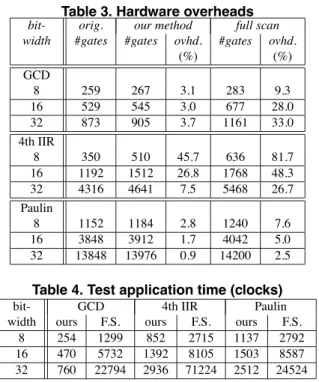
Table 3. Hardware overheads bit- orig. our method full scan width #gates #gates ovhd. #gates ovhd.
(%) (%)
GCD
8 259 267 3.1 283 9.3
16 529 545 3.0 677 28.0
32 873 905 3.7 1161 33.0
4th IIR
8 350 510 45.7 636 81.7
16 1192 1512 26.8 1768 48.3
32 4316 4641 7.5 5468 26.7
Paulin
8 1152 1184 2.8 1240 7.6
16 3848 3912 1.7 4042 5.0
32 13848 13976 0.9 14200 2.5
Table 4. Test application time (clocks)
bit- GCD 4th IIR Paulin
width ours F.S. ours F.S. ours F.S.
8 254 1299 852 2715 1137 2792
16 470 5732 1392 8105 1503 8587
32 760 22794 2936 71224 2512 24524 Table 3 shows hardware overhead of the DFT methods. Column orig.,our method and F.S. lists the number of gates in the data paths before DFT, after DFT in proposed method and after DFT in full scan method, respectively. In all exam- ples, our DFT method has lower hardware overhead (ovhd.) than the full scan method. However, the results in the case of 4th IIR are not as impressive as in other cases, because the data path includes three operational modules, each of which has a single input port and executes multiplication with a constant. Since these operational modules are mod- ified so that the modules realize the thru functions.8 This result suggests that the hardware overhead caused by a re- alization of thru function without mask is not so high.
Table 4 shows test application time for three small data paths. We determine the time by the number of clocks re- quired to apply all the generated test patterns and to observe the responses.
Table 5 shows the characteristics and result of a data path of a RISC processor. This circuit has 59773 gates before
8We made modification independently of the constant values. We can attain less hardware overhead if we consider the constant values.
Table 5. Characteristics & results of RISC (a)Characteristics
#PIs #POs #registers #MUXs #op.s
1 2 40 83 24
(b)Results
TGT(sec.) HW(%) TAT(clk.)
ours 58.55 10.9 8390
FS 219.5 14.8 701987
DFT. In this table, TGT, HW, and TAT denote the test gen- eration time, hardware overhead and test application time ,respectively. Even for the large and practical circuit, the proposed method is superior to full scan in all items.
6. Conclusions
In this paper, we proposed a new DFT method for RTL data paths to achieve 100% fault efficiency. The DFT method is based on hierarchical test and usage of a com- binational ATPG tool. Experimental results show that our DFT method achieves 100% fault efficiency with low hard- ware overhead, has shorter test generation time (especially for the large circuits) than the traditional full scan method, and improves test application time drastically compared with the full scan method.
Acknowledgments: This work was supported in part by Semiconductor Technology Academic Research Center (STARC) under the Research Project and in part by the Min- istry of Education, Science, Sports and Culture, Japan under Grant-in-Aid for Scientific Research B(2)(No.09480054). Authors would like to thank Tomoo Inoue of Hiroshima City University and Michiko Inoue of Nara Institute of Sci- ence and Technology for their helpful discussion.
References
[1] Petra Michel, Ulrich Lauther and Peter Duzy: The synthesis approach to digital system design, Kluwer academic publish- ers groupe, Dordrecht, 1992
[2] B.T.Murray and J.H.Hayes: “Hierarchical test generation us- ing pre computed tests for modules,” IEEE Trans. on CAD, vol. 9,No. 6, pp.594-603,June, 1990.
[3] R.B.Norwood and E.J.McCluskey: “Orthogonal scan: Low overhead scan for data paths”, Proc. 1996 Int. Test Conf., pp.659-668, 1996
[4] R.B.Norwood and E.J.McCluskey: “High-level synthesis for orthogonal scan,” Proc. 15th VLSI Test Symp, pp370-375 ,1997
[5] S.Bhatia and N.K.Jha: “Genesis: A behavioral synthesis sys- tem for hierarchical testability,” Proc. European Design and Test Conference, pp272-276 , 1994
[6] I.Ghosh,A.Raghunath and N.K.Jha: “Design for hierarchical testability of RTL circuits obtained by behavioral synthesis,” Proc. 1995 IEEE Int. Conf. on Computer Design,pp.173-179 , 1995
[7] I.Ghosh,A.Raghunath and N.K.Jha: “A design for testability techinique for RTL circuits using control/dataflow extraction” Proc. 1996 IEEE/ACM Int.Conf.on CAD,pp.329-336,1996 [8] S. Bhattacharya and S. Dey: “A High-Level Alternative to
Full-Scan Testing with Reduced Area and Test Application Time,” Proc. the IEEE VLSI Test Sympo.,pp.74-80,1996 [9] T. Masuzawa, H. Wada, K. K. Saluja and H. Fujiwara: “
A non-scan DFT method for RTL data paths to archieve complete fault efficiency,” Information Science Technical Re- port:TR98009, Nara Institute of Science and Technology, 1998