Strongly Secure Scan Design Using Extended Shift
Registers
Hiroshi Yamazaki
1, Toshinori Hosokawa
1and Hideo Fujiwara
21College of Industrial Technology Nihon University
Chiba, 275-8575, JAPAN
{yamazaki.hiroshi, toshinori.hosokawa}@nihon-u.ac.jp
2Faculty of Informatics Osaka Gakuin University Osaka, 564-8511, JAPAN
Abstract—Full scan designs have been proposed as the most popular design-for-testability technique. However, the contents of flip-flops can be easily controlled and observed in full scan designs, hence a high risk of information disclosure by scan-based side- channel attacks has been pointed out. To solve this problem, strongly secure designs for generalized shift registers have been proposed. In this paper, we consider extended shift registers instead of generalized shift registers, and propose how to design strongly secure circuits for extended shift registers that are shift register equivalent (SR- equivalent, for short).
Keywords—scan design; extended shift register; strongly secure; shift register equivalents; scan-based side-channel attack; security.
1. INTRODUCTION
It is important to design circuits that satisfy both security and testability for VLSI including cryptographic circuits. Full scan designs [1] that provide high controllability and observability have been proposed as the most popular design- for-testability (DFT) techniques. Therefore, full scan designs and scan testing ensure high testability and high fault coverage. However, the contents of flip-flops (FFs) can be easily controlled and observed in full scan designs, hence a high risk of information disclosure by scan-based side-channel attacks [2] has been pointed out.
To deter scan-based side-channel attacks, several secure scan design methods [3-15] have been proposed. A secure and testable scan design approach by using extended shift registers called “SR-equivalents” that are functionally equivalent but not structurally equivalent to a shift register (SR, for short) was proposed in [10]. Although the output sequence becomes the same as the input sequence for an SR-equivalent extended SR, the internal state (state of FFs) differs from that of a shift register (SR). Hence, it is difficult for the attacker to identify the structure of the extended SR [10].
However, a state assignment of extended SRs might equal that of SRs. When such a state assignment exists, it might happen that the attacker succeeds in initializing the states of extended SRs and/or observing the states of extended SRs [14,15]. To avoid such leakage, a new secure concept called strongly secure was proposed in [14]. All state assignments of strongly secure circuits are different from those of SRs, hence
strongly secure circuits are more secure than SR-equivalent circuits. The method of [10] includes non-strongly secure circuits because of considering only SR-equivalent circuits. Thus, strongly secure designs can further improve the security of SR-equivalent extended SRs. On the other hand, the papers of [14,15] proposed how to design strongly secure circuits for SR-equivalent generalized shift registers. The paper of [14] proposed the method to generate SR-equivalent and strongly secure circuits for SR-equivalent generalized feed-forward shift registers (GF2SR). The paper of [15] proposed the method to generate SR-equivalent and strongly secure circuits for SR- equivalent generalized feedback shift registers (GFSR).
In this paper, we consider extended shift registers instead of generalized shift registers and propose how to design strongly secure circuits for extended shift registers that are SR- equivalent. When a given SR-equivalent extended SR becomes non-SR-equivalent after making it strongly secure, it can be recovered to be SR-equivalent. Our proposed method ensures to design SR-equivalent and strongly secure extended SRs.
2. EXTENDED SHIFT REGISTRERS AND SR-EQUIVALENT CIRCUITS
A. Extended Shift Registers
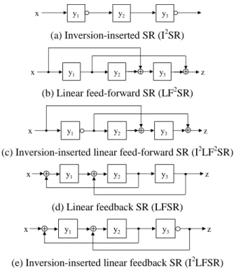
An extended shift register is a linear structured shift register with/without feedback, feed-forward and/or inverters. We consider five types of extended shift registers as shown in Fig.1. They are inversion-inserted SRs (I2SR), linear feed-forward SRs (LF2SR), inversion-inserted linear feed-forward SRs (I2LF2SR), linear feedback SRs (LFSR), and inversion-inserted linear feedback SRs (I2LFSR).
B. SR-Equivalent Circuits
Consider a circuit C with a single input x, a single output z, and k flip-flops. C is called functionally equivalent to a k-stage shift register (or SR-equivalent) if the input value applied to x at any time t appears at z after k clock cycles, i.e., z(t+k)=x(t) for any time t.
Figure 2 shows an example of an SR-equivalent circuit (LF2SR, R1) and a result of symbolic simulation for R1.
17th IEEE Workshop on RTL and High Level Testing (WRTLT'16), Nov. 2016.
(a) Inversion-inserted SR (I2SR)
(b) Linear feed-forward SR (LF2SR)
(c) Inversion-inserted linear feed-forward SR (I2LF2SR)
(d) Linear feedback SR (LFSR)
(e) Inversion-inserted linear feedback SR (I2LFSR) Figure 1. Extended shift registers
Consider the R1, given in Figure 2(a). By using symbolic simulation, we can obtain an output sequence (z(t)=y1(t) ⊕ y3(t), z(t+1)=y2(t), z(t+2)=y1(t), z(t+3)=x(t)) as shown in Figure 2(b). From Figure 2(b), the input value x(t) of time t appears at output z(t+ 3)= x(t) after 3 clock cycles. Therefore, R1 is SR- equivalent.
3. STRONGLY SECURE CIRCUITS
In this paper, we assume that attackers do not know gate- level designs in detail, and that attackers knows the presence of test pins (scan in/out, scan, and reset) and modified scan chains. However, they do not know the structure of extended scan chains.
Even if an extended SR is SR-equivalent, some state assignments of the extended SR might be equal to those of a shift register. In this case, it might happen that the attacker succeeds in initializing the states of the extended SR and/or observing the states of the extended SR [14, 15].
Consider again the 3-stage LF2SR, R1, in Fig. 2(a) and the result of symbolic simulation shown in Fig. 2 (b). When y1(t+3) = 0, it holds that (y3(t+3), y2(t+3), y1(t+3)) = (x(t), x(t+1), x(t+2)), i.e., by any input sequence (x(t), x(t+1), x(t+2)), the final state ((y3(t+3), y2(t+3), y1(t+3)) is transferred to (x(t), x(t+1), x(t+2)) when y1(t+3) = 0. For example, when by input sequence (x(t)=0, x(t+1)=0, x(t+2)=0), the final state of R1 is transferred to (y3(t+3)=0, y2(t+3)=0, y1(t+3)=0)) after 3-clock cycles, i.e., the final state (y3(t+3), y2(t+3), y1(t+3)) equals to (x(t), x(t+1), x(t+2)) when (x(t)=0, x(t+1)=0, x(t+2)=0). This means R1 behaves in the same way as a shift register during scan-in operation when y1(t+3) = 0. Thus, it is not secure when attackers regard R1 as a shift register and try to initialize it. Similarly, when y1(t) = 0, it holds that (y1(t), y2(t), y3(t)) = (z(t+2), z(t+1), z(t)), i.e., the output sequence (z(t), z(t+1),
z(t+2)) equals to (y3(t), y2(t), y1(t)) when y1(t) = 0. This means R1 behaves in the same way as a shift register during scan-out operation when y1(t) = 0. Thus, it is not secure when attackers regard R1 as a shift register and try to observe a state of R1. In this way, it might happen that attackers succeed in initializing the states of R1 and/or observing the states of R1. To avoid such information leakage, [14] proposed a new secure concept called strongly secure.
Consider a circuit C with a single input x, a single output z, and k-flip-flops. C is called to be scan-in secure if for any internal states of C a transfer sequence (of length k) to the state (final state) is always different from that of a k-stage shift register [14]. C is called to be scan-out secure if for any present
(a) LF2SR, R1
(b) Symbolic simulation
Figure 2. Example of non-strongly secure SR-equivalent circuit
(a) I2LF2SR, R2
(b) Symbolic simulation
Figure 3. Example of strongly secure circuit
y1 y2 y3
x
y1 y2 y3
x z
y1 y2 y3
x z
x y1 y2 y3 z
x y1 y2 y3 z
y1 y2 y3
x z
x y1 y2 y3 z
x(t) y1(t) y2(t) y3(t) z(t) = y1(t)⊕y3(t) x(t+1) x(t) y1(t) x(t)⊕y2(t) z(t+1) = y2(t) x(t+2) x(t+1) x(t) x(t+1) ⊕y1(t) z(t+2) = y1(t) x(t+3) x(t+2)
= y1(t+3)
x(t+1)
= y2(t+3)
x(t+2) ⊕x(t)
= y3(t+3)
z(t+3) = x(t)
x(t) = y3(t+3)⊕x(t+2)
= y3(t+3)⊕y1(t+3) x(t+1) = y2(t+3) x(t+2) = y1(t+3)
y1(t) = z(t+2) y2(t) = z(t+1) y3(t) = z(t)⊕y1(t)
= z(t)⊕z(t+2)
y1 y2 y3
x z
x y1 y2 y3 z
x(t) y1(t) y2(t) y3(t) z(t) = y1(t)⊕y3(t) ⊕1 x(t+1) x(t) y1(t)⊕1 x(t)⊕y2(t) z(t+1) = y2(t)⊕1 x(t+2) x(t+1) x(t)⊕1 x(t+1) ⊕y1(t) ⊕1 z(t+2) = y1(t) x(t+3) x(t+2)
= y1(t+3)
x(t+1)⊕1
= y2(t+3)
x(t+2) ⊕x(t) ⊕1
= y3(t+3)
z(t+3) = x(t)
x(t) = y3(t+3)⊕x(t+2)⊕1 x(t+1) = y2(t+3)⊕1 x(t+2) = y1(t+3)
y1(t) = z(t+2) y2(t) = z(t+1)⊕1 y3(t) = z(t)⊕y1(t)⊕1
Figure 4. Design for strongly secure (I2)LF2SRs states of C the output sequence of length k is always different from that of a k-stage shift register [14]. C is called to be strongly secure if C is scan-in secure and scan-out secure [14].
Consider again the LF2SR, R1 and the result of symbolic simulation shown in Fig.2. As illustrated in Fig.2 (b), the final state equals to the input sequence when y1(t+3) = 0. Thus, R1 is not scan-in secure. Similarly, the initial state equals to the output sequence when y1(t) = 0. Thus, R1 is not scan-out secure. Therefore, R1 is not strongly secure. Figure 3 shows an example of a strongly secure circuit (LF2SR, R2) and a result of symbolic simulation for R2. By using symbolic simulation, we can obtain an output sequence (z(t+2)=y1(t),z(t+1)=y2(t) ⊕ 1, z(t)=y1(t) ⊕ y3(t) ⊕ 1) and final state of R2 transfers (y1(t+3)=x(t+2),y2(t+3)=x(t+1)⊕1,y3(t+3)=x(t+2)⊕x(t)⊕1). From the result of symbolic simulation shown in Fig. 3(b), we can see y2(t+3) never equals x(t+1). Thus, R2 is scan-in secure. Similarly, we can see z(t+1) never equals y2(t), which implies R2 is scan-out secure. Therefore, R2 is strongly secure. For any SR-equivalent circuit, the following Theorem 1 holds.
Theorem 1: For any SR-equivalent circuit C, if C is scan-in secure, C is scan-out secure, and vice versa.
(Proof) Consider a circuit C with a single input x, a single output z, and k flip-flops y1, y2, …, yk. Let x(t) and z(t) be the input value and the output value at time t, and let (y1(t), y2(t),
…, yk(t)) be the state of FFs at time t. Suppose an input sequence x(t), x(t+1), …, x(t+k-1) is applied to C. After this input sequence is applied, the state becomes (y1(t+k), y2(t+k),
…, yk(t+k)). The output sequence of length k after time t+k becomes z(t+k), z(t+k+1), …, z(t+2k-1). Here, since C is SR- equivalent, z(t+k)=x(t), z(t+k+1)=z(t+1), …, z(t+2k-1)=x(t+k- 1).
(Necessary condition) If we assume that C is not scan-out secure, there exist an output sequence (z(t+k)=yk(t+k), …, (t+2k-1)=y1(t+k)) and a state (y1(t+k), y2(t+k), …, yk(t+k)). However, since C is SR-equivalent, the output sequence is (z(t+k)=x(t), z(t+k+1)=x(t+1), … , z(t+2k-1)=x(t+k-1)). Therefore, C is not scan-in secure because there exists a state such that (y1(t+k), y2(t+k), …, yk(t+k)) = (x(t+k-1), x(t+k-2),
…, x(t)).
(Sufficient condition) If we assume that C is not scan-in secure, there exist an input sequence (x(t)=yk(t+k), …, x(t+k- 1)=y1(t+k)) and a state (y1(t+k), y2(t+k), …, yk(t+k)). However, since C is SR-equivalent, the output sequence is (z(t+k)=x(t), z(t+k+1)=x(t+1), …, z(t+2k-1)=x(t+k-1)). Therefore, C is not scan-out secure because there exist a state such that (y1(t+k), y2(t+k), …, yk(t+k)) = (z(t+2k-1), z(t+2k-2), …, z(t+k)). (Q.E.D)
(a) I2LF2SR, R3
(b) Symbolic simulation
Figure 5. Losing SR-Equivalence by inserting NOT gate
(a) I2LF2SR, R4
(b) Symbolic simulation
Figure 6. Strongly secure design by inserting NOT gate 4. HOW TO DESIGN STRONGLY SECURE LF2SRS AND
I2LF2SRS
In this section, we propose how to design strongly secure LF2SR and I2LF2SR. From Theorem 1, we can see that in order to design a strongly secure circuit, we only need to modify a given circuit so that it becomes either scan-in secure or scan- out-secure.
Consider an (I2)LF2SR C with a single input x, a single output y, and k flip-flops y1, y2, …, yk, such that the most left XOR gate is located between yp and yp+1 as shown in Fig.4. As illustrated in Fig.4, if there is at least one NOT gate between primary input x and flip-flop yp, the final state (y1, y2,
…, yk) of C is always different from that of SR. Hence, we can see C is scan-in secure. However, if the change of logic value by inserting NOT gate propagates to primary output z, C loses b e i n g S R - e q ui v a l e n t . I n t h i s c a s e , a N O T g a t e i s
Insert at least one NOT gate
in this interval The most left XOR
y1 yp yp+1
x
… … ykz
y
1y
2y
3x z
The influence of a NOT gate insertion propagates
x y1 y2 y3 z
x(t) y1(t) y2(t) y3(t) z(t) = y1(t)⊕y3(t) x(t+1) x(t) y1(t)⊕1 x(t)⊕y2(t) z(t+1) = y2(t) x(t+2) x(t+1) x(t)⊕1 x(t+1) ⊕y1(t) ⊕1 z(t+2) = y1(t)⊕1 x(t+3) x(t+2)
=y1(t+3)
x(t+1)⊕1
=y2(t+3)
x(t+2) ⊕x(t) ⊕1
=y3(t+3)
z(t+3) = x(t)⊕1
y
1y
2y
3x z
The influence of a NOT gate insertion counteracts
x y1 y2 y3 z
x(t) y1(t) y2(t) y3(t) z(t) = y1(t)⊕y3(t) ⊕1 x(t+1) x(t) y1(t)⊕1 x(t)⊕y2(t) z(t+1) = y2(t)⊕1 x(t+2) x(t+1) x(t)⊕1 x(t+1) ⊕y1(t) ⊕1 z(t+2) = y1(t) x(t+3) x(t+2)
=y1(t+3)
x(t+1)⊕1
=y2(t+3)
x(t+2) ⊕x(t) ⊕1
=y3(t+3)
z(t+3) = x(t)
Figure 7. Design for strongly secure (I2)LFSRs
additionally inserted between flip-flop yp+ 1 and primary output z so that C becomes SR-equivalent.
Figure 5 illustrates I2LF2SR, R3 that lost SR-equivalence by inserting NOT gate and the result of symbolic simulation for R3. Figure 5(a) is an I2LF2SR for which one NOT gate is inserted at input side of flip-flop y2 of R1. From the symbolic simulation of Fig. 5(b), we can see y2(t+3) never equals x(t+1). Thus, R3 is scan-in secure. Furthermore, from Theorem 1, we can see R3 is strongly secure. However, we can see R3 is not SR-equivalent because of z(t+3)=x(t) ⊕ 1. That means the influence of inserting NOT gate for the input side of y2 propagates primary output z. For this reason, we need to additionally insert a NOT gate between flip-flop y2 and primary output z to counteract the influence of NOT gate.
The R4 shown in Fig. 6(a) is a result by inserting two NOT gates. Fig. 6(b) shows the result of symbolic simulation for R4. The change of parity by inserting a NOT gate into the input side of flip-flop y2 is counteracted by inserting a NOT gate into the output side of flip-flop y3. From the symbolic simulation in Fig. 6(b), we can see input value x(t) equals output value z(x+3), which implies R4 is SR-equivalent. We can see y2(t+3) never equals x(t+1). Thus, R4 is scan-in secure. Therefore, R4 is strongly secure.
For a given SR-equivalent LF2SR or I2LF2SR, we present how to make it strongly secure as follows.
Method for making SR-equivalent LF2SRs/I2LF2SRs strongly secure:
Step(1) : If there is no NOT gate between primary input x and flip-flop yp (see Fig.4), at least one NOT gate is inserted between them so that C becomes scan-in secure.
Step(2) : If C is not SR-equivalent due to the NOT gate insertion in Step(1), the path of parity change by the NOT gate insertion is analyzed. From the result of analysis, a NOT gate is additionally inserted between flip-flop yp and primary output z to counteract the change of parity so that C becomes SR-equivalent.
5. HOW TO DESIGN STRONGLY SECURE LFSRS AND I2LFSRS
In this section, we propose how to design strongly secure LFSR and I2LFSR. From Theorem 1, we can see that in order to design a strongly secure circuit, we only need to modify a
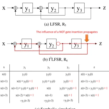
(a) LFSR, R5
(b) I2LFSR, R6
(c) Symbolic simulation
Figure 8. Losing SR-Equivalence by inserting NOT gate
given circuit so that it becomes either scan-in secure or scan- out-secure.
Consider an (I2)LFSR C with a single input x, a single output y, and k flip-flops y1, y2, …, yk, such that the most right XOR gate is located at the input of yq as shown in Fig.7. As illustrated in Fig.7, if there is at least one NOT gate between flip-flop yq and primary output z, the final state (y1, y2, …, yk) of C is always different from that of SR. Hence, we can see C is scan-out secure. However, if the change of logic value by inserting NOT gate propagates to primary output z, C loses being SR-equivalent. In this case, a NOT gate is additionally inserted between primary input x and flip-flop yq, so that C becomes SR-equivalent.
Fig. 8(a) shows an example of an SR-equivalent LFSR, R5
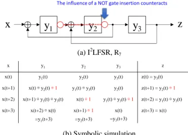
that is not strongly secure. Fig. 8(b) shows an example of I2LFSR, R6 that is obtained by inserting a NOT gate to the output of y2 of R5. Fig. 8(c) shows a result of symbolic simulation for R6. From the symbolic simulation in Fig. 8(c), we can see y3(t+3) never equals x(t). Thus, R6 is scan-in secure. Similarly, we can see z(t+1) never equals y2(t). Hence, R6 is scan-out secure. Therefore, R6 is strongly secure. However, we can see R6 is not SR-equivalent because of z(t+3)=x(t) ⊕ 1. That means the influence of the NOT gate insertion for the output side of y2 propagates primary output z. For this reason, we need to additionally insert a NOT gate between primary input x and flip-flop y2 to counteract the influence of NOT gate. The circuit R7 shown in Fig. 9(a) is the result by inserting two NOT gates. Fig. 9(b) shows the result of symbolic simulation for R7. The change of parity by inserting a NOT gate into the output of the flip-flop y2 is counteracted by inserting a NOT gate into the output of the flip-flop y1. From
y
q-1y
q …y
kz
Insert at least one NOT gate in this interval
…
The most right XOR
y
1x
x y z
1
y
2y
3x y
1y
2y
3z
The influence of a NOT gate insertion propagates
x y1 y2 y3 z
x(t) y1(t) y2(t) y3(t) z(t) = y3(t)
x(t+1) x(t)⊕y2(t) ⊕1 y1(t)⊕y3(t) y2(t) ⊕1 z(t+1) = y2(t)⊕1 x(t+2) x(t+1) ⊕y1(t)⊕y3(t) ⊕1 x(t) y1(t)⊕y3(t) ⊕1 z(t+2) = y1(t)⊕y3(t) ⊕1 x(t+3) x(t+2)⊕x(t) ⊕1
=y1(t+3)
x(t+1)
=y2(t+3)
x(t) ⊕1
=y3(t+3)
z(t+3) = x(t)⊕1
(a) I2LFSR, R7
(b) Symbolic simulation
Figure 9. Making strongly secure by inserting NOT gate
the symbolic simulation in Fig. 9(b), we can see the input value x(t) equals the output value z(x+3), which implies R7 is SR- equivalent. We can further see z(t+1) never equals y2(t). Thus, R7 is scan-out secure. Therefore, R7 is strongly secure.
For a given SR-equivalent LFSR or I2LFSR, we present how to make it strongly secure as follows
Method for making SR-equivalent LFSRs/I2LFSRs strongly secure:
Step(1) : If there is no NOT gate between flip-flop yq and primary output z (see Fig.7), at least one NOT gate is inserted between them so that C becomes scan-out secure.
Step(2) : If C is not SR-equivalent due to the NOT gate insertion in Step(1), the path of parity change by the NOT gate insertion is analyzed. From the result of analysis, a NOT gate is additionally inserted between primary output z and flip-flop yq to counteract the change of parity so that C becomes SR-equivalent.
6. CONCLUSION
In this paper, we proposed how to design strongly secure circuits for four classes of extended shift registers that are SR- equivalent; LF2SR, LFSR, I2LF2SR, and I2LFSR. When a given SR-equivalent extended SR becomes non-SR-equivalent after making it strongly secure, it can be recovered to be SR- equivalent. Our proposed method ensures to design SR- equivalent and strongly secure extended SRs. Furthermore,
from Theorem 1, we proved that if an SR-equivalent circuit is scan-in secure, it is scan-out secure, and vice versa. Thanks to this theorem, we presented efficient methods for designing strongly secure and SR-equivalent extended SRs.
Future work includes analyzing the cardinality of several classes for strongly secure and SR-equivalent extended SRs, and clarifying those security levels.
REFERENCES
[1] H.Fujiwara, Logic Testing and Design for Testability, The MIT Press, 1985.
[2] B.Yang, K.Wu, and R.Karri, "Scan based side channel attack on dedicated hardware implementations of data encryption standard," International Test Conference 2004, pp.339-344, 2004.
[3] D.Hély, F.Bancel, M.-L.Flottes, and B.Rouzeyre, "Securing scan control in crypto chips," Journal of Electronic Testing, vol.23, no.5, pp.457-464, Oct. 2007.
[4] B.Yang, K.Wu, and R.Karri, "Secure Scan: A Design-for-Test Architecture for Crypto Chips," IEEE Trans. Comput.-Aided Des. Integr. Circuits Syst., vol.25, no.10, pp.2287-2293, 2006.
[5] J.Lee, M.Tehranippr, C.Patel, and J.Plusquellic, "Securing Designs against Scan-Based Side-Channel Attacks," IEEE Trans. Dependable and Secure Computing, vol.4, no.4, pp.352-336, 2007.
[6] S.Paul, R.S.Chakraborty, and S.Bhunia, "VIm-Scan: A Low Overhead Scan Design Approach for Protection of Secret Key in Scan-Based Secure Chips," Proc. 25th IEEE VLSI Test Symposium, pp.455-460, 2007.
[7] G.Sengar, D.Mukhopadhyay, and D.R.Chowdhury, "Secured Flipped Scan-Chain Model for Crypto-Architecture," IEEE Trans. Comput.- Aided Des. Integr. Circuits Syst., vol.26, no.11, pp.2080-2084, 2007. [8] U.Chandran, and D.Zhao, "SS-KTC: A High-Testability Low-Overhead
Scan Architecture with Multi-level Security Integration," Proc. 27th IEEE VLSI Test Symposium, pp.321-326, May. 2009.
[9] M.A.Razzaq, V.Singh, and A.Singh, "SSTKR: Secure and Testable Scan Design through Test Key Randomization," Proc. 20th IEEE Asian Test Symposium, pp.60-65, Nov. 2011.
[10] H.Fujiwara and M.E.J.Obien, "Secure and testable scan design using extended de Bruijn graphs," Proc. 15th Asia and South Pacific Design Automation Conference, pp.413-418, 2010
[11] K.Fujiwra and H.Fujiwara, and H.Tamamoto, "Secure and testable scan design utilizing shift register quasi-equivalents," IPSJ Trans. System LSI Design Methodology, vol.6, pp.27-33. 2013.
[12] K.Fujiwra and H.Fujiwara, "WAGSR: Web application for generalized feed forward shift registers," Proc. 13th IEEE Workshop on RTL and High Level Testing, pp.1.2.1-1.2.7, 2012.
[13] K.Fujiwara and H.Fujiwara, "Generalized feed-forward shift registers and their application to secure scan design," IEICE Trans. Inf. & Syst., vol.E96-D, no.5, pp.1125-1133, 2013.
[14] H.Fujiwara and K.Fujiwara, "Strongly secure scan design using generalized feed forward shift registers," IEICE Trans. Inf. & Syst., vol.E98-D, no.10, pp.1852-1855, Oct. 2015.
[15] H.Fujiwara and K.Fujiwara, "Properties of Generalized Feedback Shift Registers for Secure Scan Design," IEICE Trans. Inf. & Syst., vol.E99-D, no.4, pp.1255-1258, Apr. 2016.
x y
1y
2y
3z
The influence of a NOT gate insertion counteracts
x y1 y2 y3 z
x(t) y1(t) y2(t) y3(t) z(t) = y3(t)
x(t+1) x(t)⊕y2(t) ⊕1 y1(t)⊕y3(t) y2(t) z(t+1) = y2(t)⊕1 x(t+2) x(t+1) ⊕y1(t)⊕y3(t) x(t)⊕1 y1(t)⊕y3(t) ⊕1 z(t+2) = y1(t)⊕y3(t)
x(t+3) x(t+2)⊕x(t)
=y1(t+3)
x(t+1)⊕1
=y2(t+3)
x(t)
=y3(t+3)
z(t+3) = x(t)
![Figure 4. Design for strongly secure (I 2 )LF 2 SRs states of C the output sequence of length k is always different from that of a k-stage shift register [14]](https://thumb-ap.123doks.com/thumbv2/123deta/5751925.26950/3.893.468.826.89.370/figure-design-strongly-output-sequence-length-different-register.webp)