Regular Paper
A Non-scan DFT Method at Register-Transfer Level
to Achieve 100% Fault Efficiency
Satoshi Ohtake,† Hiroki Wada,†† Toshimitsu Masuzawa††† and Hideo Fujiwara†
This paper presents a non-scan design-for-testability (DFT) method for VLSIs designed at register-transfer level (RTL) to achieve complete fault efficiency. In RTL design, a VLSI generally consists of a controller and a data path. The proposed method mainly consists of the following two steps. First, DFT methods are applied to the controller and the data path, separately. Then, a test plan generator is appended to support at-speed testing. The test plan generator generates a sequence of test control vectors for the modified data path. Our experimental results show that the proposed method can significantly reduce both the test generation time and the test application time in comparison with full-scan design, though the hardware overhead of our method is slightly larger than that of full-scan design.
1. Introduction
With advances in semiconductor technology, the complexity of VLSI designs is growing and the cost of testing is increasing. Therefore, it is necessary to reduce the test generation time and test application time. To reduce the com- plexity of test generation, design-for-testability (DFT) techniques have been proposed. The most commonly used DFT techniques for se- quential circuits are scan-based approaches5). These techniques modify sequential circuits so that automatic test pattern generation (ATPG) tools can achieve high fault efficiency☆in a rea- sonable time. However, the techniques sacrifice the possibility of at-speed testing10) for fault efficiency enhancement. To avoid this disad- vantage of scan techniques, several non-scan approaches have been investigated. Moreover, since techniques of test generation and DFT at gate level face problems arising from the huge number of elements and the high complexities of the circuits at gate level, several techniques for test generation and DFT at register-transfer level (RTL) have recently been proposed.
In RTL design, a VLSI circuit generally con- sists of two separate parts: a controller part and a data path part. The former is represented by a state transition graph (STG) and the lat- ter by hardware elements (e.g., registers, mul-
† Graduate School of Information Science, Nara Insti- tute of Science and Technology
†† Central Research Laboratory, Hitachi Ltd.
††† Department of Computer Science, Graduate School of Information Science and Technology, Osaka Uni- versity
tiplexers, and operational modules) and lines. A controller and a data path are connected by internal signals: control signals and status sig- nals. Most DFT methods for RTL circuits are concerned with only data paths or controllers, under the assumption that the control signals and the status signals are directly controllable and observable from outside the VLSI.
For controllers, Chakradhar, et al.3) pro- posed a non-scan DFT method at RTL. This method can achieve high fault efficiency but cannot always guarantee complete (100%) fault efficiency. Furthermore, it is applicable only to PLA-based sequential circuits. References 14) and 4) proposed non-scan DFT methods which achieve 100% fault efficiency, respectively. In these methods, given an STG, a sequential cir- cuit is first synthesized from it. Then, for the combinational part of the synthesized sequen- tial circuit, test patterns are generated by us- ing a combinational ATPG tool. Most of the generated test patterns can be applied to the sequential circuit by using state transitions of the STG. However, there may exist test pat- terns which cannot be applied using state tran- sitions of the STG. In this case, an extra logic is appended, which provides the extra transitions required for testing. The above mentioned test patterns are applied by using the extra logic.
For data paths, several non-scan DFT meth- ods at RTL have been reported, e.g., orthogo- nal scan12),13) and H-SCAN1), which use nor-
☆ Fault efficiency is the ratio of the number of faults detected or proved redundant to the total number of faults.
1266
mal data path flow as a scan path instead of the traditional scan path flow. These methods can reduce the hardware overhead and test ap- plication time in comparison with full-scan de- sign☆. However, the test generation time can- not be reduced, because the test generation ap- proach is the same as in full-scan design. To re- duce the test generation time, a hierarchical test generation approach was proposed by Murray and Hayes11). The hierarchical test generation of a data path consists of the following two steps: for individual combinational hardware elements, generate test patterns at gate level and generate test plans at RTL, where a test plan is a control sequence to propagate test pat- terns from the primary inputs to the inputs of the respective hardware elements and to prop- agate responses from the output of the respec- tive hardware elements to the primary outputs. Genesis2),6)∼8)is an approach based on such hi- erarchical test generation for data paths. How- ever, it cannot always guarantee 100% fault ef- ficiency, even if 100% fault efficiency is achieved for combinational test generation of each indi- vidual combinational hardware element, due to the backtracking in the test plan generation for large data paths. Reference 15) presented a DFT method based on such hierarchical test generation and strong testability. Strong testa- bility is a property of data paths which guaran- tees that test plans will be generated for all the combinational hardware elements of the data path. According to the method of Ref. 15), test plans can be derived with complexity O(n2), where n is the number of hardware elements in an RTL data path.
This paper presents a DFT method for an RTL circuit consisting of a controller part and a data path part. Given an RTL controller- data path circuit, we apply the DFT method of Ref. 14) to the controller part and apply that of Ref. 15) to the data path part. The exper- imental results obtained by using the bench- mark circuits listed in Refs. 14) and 15) show that their hardware overheads were 3.5% and 4.0% on average, respectively. Their test appli- cation times were reduced on average to 25.4% and 17.6% of the times for the full-scan design, respectively. Furthermore, both of these DFT
☆ In this paper, the hardware overhead and test appli- cation time of a full-scan circuit are calculated under the assumption that the scan flip-flop consists of a multiplexer and a standard flip-flop and that all the scan flip-flops are connected to one scan chain.
methods can achieve 100% fault efficiency and allow at-speed testing. Notice that, in this pa- per, we say “100% fault efficiency is achieved” if test patterns for each combinational sub-circuit in a given circuit are generated by using a com- binational test generation algorithm and if it is guaranteed that the sub-circuits can be tested by applying all the generated patterns. Thus, all the redundant faults are only in combina- tional sub-circuits and they can be proved by a combinational test generation algorithm.
In the above-mentioned DFT methods, we as- sumed that both control signals and status sig- nals between a controller and a data path are directly controllable and observable from out- side circuits. However, if we consider a DFT method for a whole circuit consisting of both a controller and a data path, we have to remove this assumption by adding some extra logic to provide both controllability and observability of those control and status signals. In this paper, we resolve this problem by (1) adding multi- plexers on those control and status signals to connect directly from primary inputs and to primary outputs and (2) embedding an extra circuit in the controller side, called a test plan generator, which can generate test plans for the data path of an RTL circuit.
The proposed DFT method for controller- data path circuits has the following advantages:
• 100% fault efficiency can be achieved.
• At-speed testing can be performed. Furthermore, according to our experimental re- sults,
• The test application time can be reduced significantly in comparison with that of full-scan design.
• The test generation time can be reduced significantly in comparison with that of full-scan design.
• The hardware overhead is slightly large in comparison with that of full-scan design, but the difference between them is small. This paper is organized as follows: Sec- tion 2 gives a definition of controller-data path circuits. In Section 3, we introduce the DFT methods in Ref. 14) for controllers and in Ref. 15) for data paths, and propose a new DFT method for whole circuits consisting of both controllers and data paths. Section 4 re- ports experimental results obtained using the proposed method.
Controller Data Path Control Signals
(CSs)
Status Signals (SSs)
Primary Inputs (PIs)
Primary Outputs (POs) Primary Inputs (PIs)
Primary Outputs (POs)
COs CIs
SIs SOs
CIs: Control Inputs SOs: Status Outputs COs: Control Outputs
SIs: Status Inputs
Fig. 1 An RTL controller-data path circuit.
2. Preliminaries
In RTL description, a VLSI circuit gener- ally consists of a controller and a data path, as shown in Fig. 1. The former is represented by an STG and the latter is represented by hard- ware elements (e.g., registers, multiplexers, and operational modules) and lines. Both the con- troller and the data path have primary inputs from the outside of the VLSI and primary out- puts to the outside of the VLSI. The controller also has status inputs from the data path and control outputs to the data path. Similarly, the data path has control inputs from the controller and status outputs to the controller. The sig- nals from the control outputs to the control in- puts are called control signals, and the signals from the status outputs to the status inputs are called status signals.
Data Path
A data path consists of hardware elements and lines. A hardware element is a primary in- put, a primary output, a control input, a status output, a register, a multiplexor, or an opera- tional module, and a line connects two hard- ware elements with some bit width. Inputs of a hardware element of a data path can be clas- sified into data inputs and control inputs. Each data input of a hardware element is connected directly or indirectly from a primary input of the data path. Control inputs of a hardware element are connected directly from control in- puts of the data path. Examples of the control inputs are load enable signals of registers, selec- tion signals of multiplexers, and function selec- tion signals of operational modules. Similarly, outputs of a hardware element of a data path can be classified into data outputs and status outputs. Each data output of a hardware ele- ment is connected directly or indirectly to a pri- mary output of the data path. Status outputs of a hardware element are connected directly to
PIs
POs
PIs
POs TMR
TPR Test Controller
Controller
ISG MUX
Data Path
Hold Mask
T P G
ACSs CSs
SSs
t0 t1
t2 t3t4
Mask
REG Hold REG HoldREG
MUX1 MUX2
MUX3 t out
Reset t1
COs
SIs
CIs
SOs ACIs
T PG: Test Plan Generator ACSs: Additional Control Signals TPR: Test Pattern Register
TMR: Target Module Register ACIs: Additional Control Inputs
ti: Test Pin
Fig. 2 Test architecture of a controller-data path circuit.
status outputs of the data path. An example of hardware elements that have status outputs is a comparator.
3. A DFT Method for RTL Controller- Data Path Circuits
3.1 Overview
In our DFT method, given a controller-data path circuit described at RTL, we first apply the DFT method of Ref. 14) to the controller and that of Ref. 15) to the data path of the cir- cuit. These DFT methods were designed by as- suming that the control signals and the status signals are directly controllable and observable from outside the circuit. However, these are internal signals between the controller and the data path in the controller-data path circuit. Thus, for testing of the controller, we have to enhance the controllability of the status inputs and the observability of the control outputs. Similarly, for testing of the data path, we have to enhance the controllability of the control in- puts and the observability of the status outputs. In the DFT method proposed in this paper, we embed mechanisms to enhance controllability and observability of the control signals and the status signals so that the testing methods of Refs. 14) and 15) can be applied. The test ar- chitecture of the controller-data path circuit of our method is shown in Fig. 2.
Before explaining the details of the test archi- tecture, we briefly introduce the DFT methods for controllers and data paths that from the ba- sis of the test architecture.
3.2 DFT for Controllers14)
In this section, we give an overview of the DFT method14) for a controller synthesized
CC
PIs POs
SR
t out t3
t4
R
ISG MUX
1
0 0
1
t3: mode switching signal t out: state output signals t4: load/hold signal
ISG: invalid test state genarator CC: combinational logic block SR: state register
SIs COs
R: reset
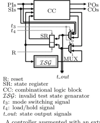
Fig. 3 A controller augmented with an extra logic ISG.
from an STG. The method achieves 100% fault efficiency with a short test generation time, and allows at-speed testing. In order to generate a test sequence that achieves 100% fault effi- ciency with a short test generation time, test patterns for the combinational part of the se- quential circuit are generated by using a combi- national ATPG tool. Each test pattern consists of the values corresponding to primary inputs (PIs), status inputs (SIs), and a state register (SR) of the sequential circuit. In order to apply a test pattern to the combinational part, it is necessary to set the corresponding value to the SR. If the value corresponds to a state reachable from the reset state of the STG, the value can be set to the SR using the original state transi- tions of the STG. Otherwise, the value cannot be set to the SR using the state transitions of the STG. In order to set such a value to the SR, we append an extra logic called an invalid test state generator (ISG) to the controller, as shown in Fig. 3. The ISG generates all the values (called invalid test states) that appear in the test patterns but that cannot be set to the SR by using state transitions of the STG. In Fig. 3, t3 is used to select the inputs of the SR (the outputs of the original combinational logic block or those of the ISG), and t4 is a load/hold signal that is utilized to reduce the test application time.
The complete fault efficiency is preserved be- cause the combinational logic block remains un- changed. The experimental results obtained us- ing benchmark circuits showed that the average hardware overhead of the ISG is only 3.5% and that the average test application time of the
method is 25.4% of that of the full-scan design given in Ref. 14).
3.3 DFT for Data Paths15) Strong Testability
Hierarchical test generation is an efficient technique for generating test patterns of very large data paths. In hierarchical test gener- ation, test generation for each combinational hardware element M proceeds as follows: Step 1: Extract M from the data path and
generate test patterns of M at logic level, using a combinational ATPG tool . Step 2: Generate a test plan that is a se-
quence of control vectors of control inputs of the data path for propagating the test patterns obtained at the first step from pri- mary inputs to the data inputs of M and for propagating responses of M from the data outputs of M to primary outputs. The test patterns and the responses are propagated by using the original data path flows of the data path.
Strong testability is proposed as a character- istic of data paths that guarantees the applica- bility of hierarchical test generation.
Definition 1 (Strong Testability15)) A data path is strongly testable iff there ex- ists a test plan for each combinational hardware element M that makes it possible to apply any pattern to M and to observe any response of M.
A strongly testable data path has the follow- ing advantages:
• Fast test pattern generation:
The test pattern generation time is short, since a combinational ATPG tool can be applied to each combinational hardware el- ement separately.
• Fast test plan generation:
The test plan generation time is short, since test plans are generated at RTL (not at gate level).
• 100% fault efficiency:
100% fault efficiency can be achieved for the whole data path, since each hardware element M is a combinational circuit of small size, and strong testability guaran- tees the complete controllability and com- plete observability of M .
The DFT Method
In the DFT method, we add no special path for propagating test patterns and responses. In- stead, test patterns and responses are propa- gated along existing data path flows. To prop-
thru
Thru
(a) using a mask element (b) using a multiplexer thru
Thru
ADDER
X1 X2
Unknown Operation
X1 X2
MUX 1 0
Fig. 4 Examples of the realization of the thru function.
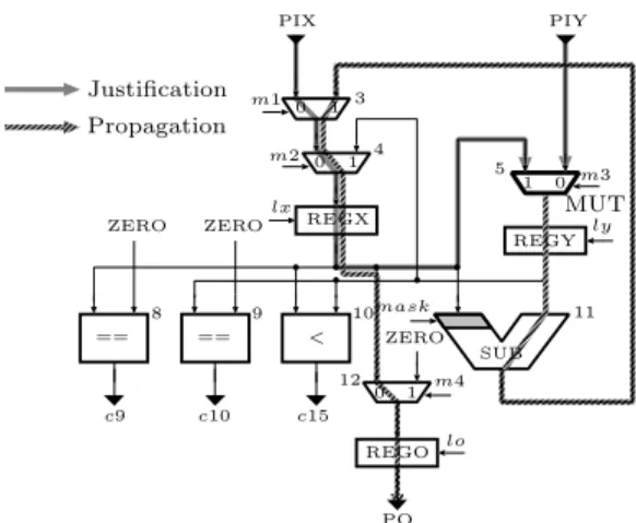
agate test patterns and responses along exist- ing data path flows, the DFT method appends thru functions to operational modules and hold functions to registers. Below we provide a brief explanation of the DFT method.
Consider the testing of a combinational hard- ware element M with two data inputs, x and y, in the data path. To test M , a value specified by a test pattern should be fed into x. We prop- agate the value along a path p from a primary input to x. If an operational module C appears on p, the output value of C will depend on the function and the input value(s) of C.
In order to propagate the value of the test pattern along p, a thru function is added to C. Most of the popular operational modules (e.g., an adder) can realize the thru function by using a mask element. The mask element generates a constant that is required to realize the thru function. Figure 4 (a) illustrates an example of such a mask element. If we cannot realize the thru function by using the mask element, we can realize it by using a multiplexer as in Fig. 4 (b).
However, we cannot achieve strong testabil- ity by adding only the thru functions. The thru functions guarantee the controllability of a sin- gle path. In the case of a hardware element which has two data inputs, a test pattern must be applied to both the inputs simultaneously. The presence of reconvergent paths in a data path can prevent such application of a test pat- tern to a hardware element which has two data inputs. In particular, this can happen if the propagation paths to the two data inputs of a hardware element start from the same primary input and have the same sequential depth. Such reconvergent paths will cause a timing conflict; that is, two different values will be required on a primary input at the same time. To resolve such conflicts, in the DFT method, some regis- ters are augmented with the hold function.
In this DFT, to control the thru functions and
REGY ly lx REGX
0 1 m2
SUB 0
1 m3
0 1 m4
REGO lo 0 1
m1
PIY
PO PIX
ZERO ZERO
== == < ZERO
c15 c10 c9
mask 3
4
5
8 9 10
12
11
MUT Justification
Propagation
Fig. 5 Example of a strongly testable data path.
the hold functions, additional control inputs are appended, as shown in Fig. 2.
An example of the application of the DFT method is shown in Fig. 5. In this example, a mask element is added to an data input of the subtracter “SUB”, and an additional con- trol input is “mask”. The time complexities of the DFT algorithm and the test plan generation algorithms are O(n) and O(n2), respectively9), where n is the number of hardware elements in the data path. These algorithms were designed for a data path such that all the wires in the data path have the same bit width. Experi- ments using benchmark circuits show that the average hardware overhead is only 4.0% and the average test application time is 17.6% of that of the full-scan design given in Ref. 15).
Test Plans
For every combinational hardware element of a data path, a test plan can be generated by the algorithm of Ref. 15). Consider a combinational hardware element M that has data inputs, con- trol inputs, data outputs, and status outputs in the data path. Each test pattern of M consists of a value corresponding to the data inputs and a value corresponding to the control inputs. We call the former a data input value and the latter a control input value. Notice that, for testing such a hardware element, we must apply test patterns to both the data inputs and the con- trol inputs. The test plan propagates the data input value to the data inputs of M from the primary inputs. It also applies a control input value to the control inputs when the data input value is justified to the data inputs. The test plan also propagates the responses that appear in the data outputs of M from the data outputs to the primary outputs. The response appear-
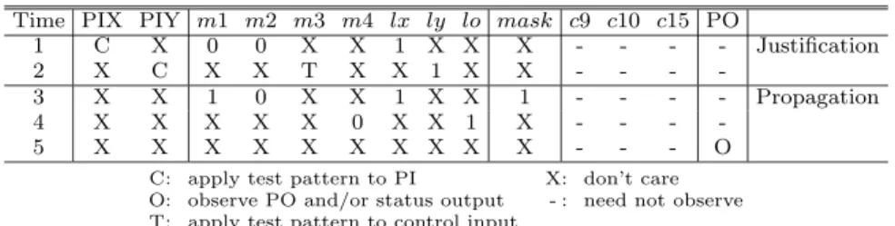
Table 1 Example of a test plan.
Time PIX PIY m1 m2 m3 m4 lx ly lo mask c9 c10 c15 PO
1 C X 0 0 X X 1 X X X - - - - Justification
2 X C X X T X X 1 X X - - - -
3 X X 1 0 X X 1 X X 1 - - - - Propagation
4 X X X X X 0 X X 1 X - - - -
5 X X X X X X X X X X - - - O
C: apply test pattern to PI X: don’t care O: observe PO and/or status output - : need not observe T: apply test pattern to control input
ing in the status outputs of M is observable from status outputs of the data path. For ex- ample, a test plan of the multiplexer marked MUT in Fig. 5 is shown in Table 1.
The computation time of the test plan gen- eration algorithm is O(n2)9), where n is the number of hardware elements in the data path. Experimental results showed that the average test application time of the method is 17.6% of that of the full-scan design in Ref. 15).
3.4 Test Architecture
3.4.1 Mechanisms for Testing of Con- trollers
The DFT method for a controller14)was de- signed by assuming that the status inputs and the control outputs of the controller are directly controllable and observable from outside the circuit, respectively. However, these are inter- nal signals in the controller-data path circuit. Thus, in the DFT proposed in this paper, the controller-data path circuit is modified so that the status signals and the control signals can be directly controlled and observed from out- side the circuit. A straightforward solution is to introduce additional test pins and to con- nect them directly to the status inputs and the control outputs. However, this solution intro- duces an unacceptable pin overhead for practi- cal design. Instead, in the proposed DFT, the pin overhead is avoided as follows: the status inputs of the controller are directly controlled from the primary inputs of the data path by adding a multiplexer “MUX1” as Fig. 2, and the control outputs of the controller are directly ob- served from primary outputs of the data path by adding a multiplexer “MUX3”. This ap- proach is acceptable because it is generally con- ceivable that the status inputs (resp. the con- trol outputs) of the controller have smaller bit- width than the primary inputs (resp. the pri- mary outputs) of the data path, and we need not use the function of the data path to test the controller. In testing of the controller, the mul- tiplexers “MUX1” and “MUX3” are configured
Table 2 Configurations of test architecture. Test Pins
t0 t1 t2 t3 t4 Operation
0 0 0 0 0 Normal operation 1 0 1 ∗ ∗ Testing controller 0 1 ∗ ∗ ∗ Testing data path
∗: Depend on test patterns or test plans
as shown in Table 2.
3.4.2 Mechanisms for Testing of Data Paths
Test plans and control input values of hard- ware elements in a data path must be applied to the control inputs (including control inputs appended by the DFT) of the data path. Sim- ilarly, the responses to the status outputs of the data path must be observed from the status outputs. If we use additional test pins to make these control inputs and status outputs directly controllable and observable, respectively, from outside controller-data path circuits, the pin overhead is unacceptable for practical designs. The problem of the pin overhead can be avoided in the following way. Here, we first consider the observability of the status outputs. In general, since the bit-width of the primary outputs of the controller is smaller than that of the sta- tus outputs, we cannot use the primary output for observing the status outputs. However, the bit-width of the primary outputs of the data path is larger than that of the status outputs. Since observation of a response of a test pat- tern only from either the status outputs or the primary inputs is sufficient, the status outputs and the primary outputs do not need to be ob- served simultaneously in testing the data path. Therefore, we can observe the status outputs by using the primary outputs of the data path. In our test architecture, this is achieved by a multiplexer “MUX3” (see Fig. 2).
We next consider the controllability of the control inputs. In general, since the number of primary inputs of the controller is smaller than that of control inputs of the data path, we cannot use the primary inputs for applying test
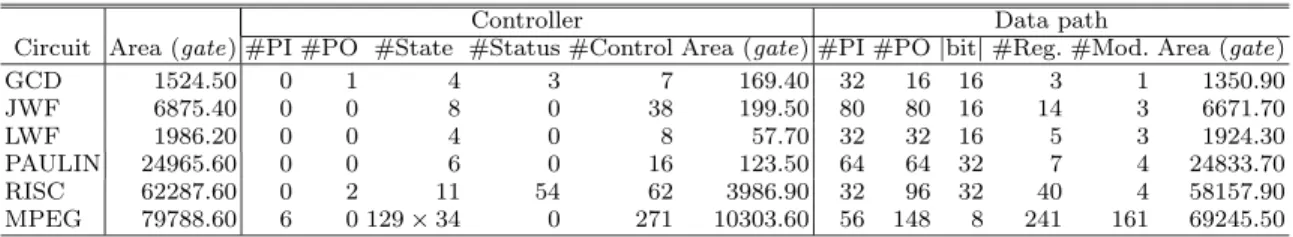
Table 3 Circuit characteristics.
Controller Data path
Circuit Area (gate) #PI #PO #State #Status #Control Area (gate) #PI #PO |bit| #Reg. #Mod. Area (gate)
GCD 1524.50 0 1 4 3 7 169.40 32 16 16 3 1 1350.90
JWF 6875.40 0 0 8 0 38 199.50 80 80 16 14 3 6671.70
LWF 1986.20 0 0 4 0 8 57.70 32 32 16 5 3 1924.30
PAULIN 24965.60 0 0 6 0 16 123.50 64 64 32 7 4 24833.70
RISC 62287.60 0 2 11 54 62 3986.90 32 96 32 40 4 58157.90
MPEG 79788.60 6 0 129 × 34 0 271 10303.60 56 148 8 241 161 69245.50
plans and control input values of hardware ele- ments to the control inputs. Moreover, in test- ing of the data path, since the primary inputs of the data path are used to apply the data in- put values of hardware elements, we cannot use them to apply the test plans and the control input values to the control inputs of the data path simultaneously. Therefore, we append an extra circuit called a test controller to generate control input values, as shown in Fig. 2.
Test Controller
Test plans are generated for the all combina- tional hardware elements in the data path of a controller-data path circuit. In our test ar- chitecture, all the test plans of the data path are generated by a test controller (Fig. 2). The test controller consists of a test plan generator (T PG), a test pattern register (TPR), and a tar- get module register (TMR) as shown in Fig. 2. Consider the testing of a combinational hard- ware element M , which has data inputs and control inputs, in the data path. The TMR is used to store the index of M . The bit width of the TMR is log m where m is the number of combinational hardware elements in the data path. The T PG generates the test plan of M from the index stored in the TMR. In other words, if the index of M is stored in the TMR, the T PG generates control vectors of the test plan of M sequentially and supplies the data path with them. When the data input value of a test pattern of M is justified to the data inputs, if some primary inputs of the data path are not used, the control input value is applied from such primary inputs by way of T PG. Oth- erwise, the control input value is pre-stored in the TPR and is applied to the control inputs by way of T PG. The load enable signal for TPR and TMR is directly connected from the reset signal of the controller. That is, if re- set is applied, TPR and TMR load values from some primary inputs of the data path; other- wise, they hold their values. The mode switch- ing signal t1is used to disable DFT elements of the data path in normal operation mode.
In testing of the data path, the advantage of using the T PG is that the test patterns of each combinational hardware element of the data path can be applied to the combinational hard- ware element at the operational speed of the circuit, because we can run the T PG using the system clock of the circuit. Notice that, since the combinational part of the T PG can be de- signed as a two-level circuit and the output of the T PG does not depend on the status of the data path, the delay of the T PG can be smaller than that of the original controller. Thus, it is conceivable that the largest delay of paths in the T PG is much less than that of the critical path in the data path.
We estimate the hardware overhead of a T PG of a controller-data path circuit. According to our experiments, the area of the T PG is almost the same as the area of the original controller of the circuit. For controller-data path circuits dominated by data flow, it is conceivable that the hardware overhead of the T PG is low.
We also consider the testing of a T PG. Since the T PG is not used in normal operation, we test the T PG only to confirm that the test plans are generated correctly. This is done by ob- serving the primary outputs of a data path (see Fig. 2).
4. Experimental Results
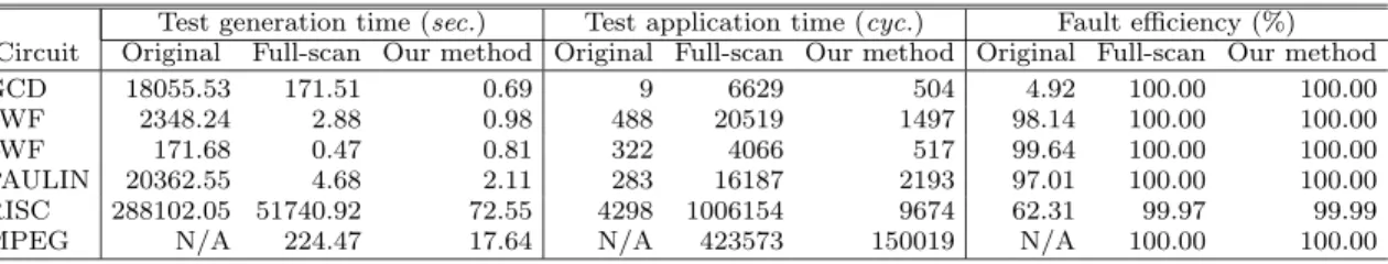
In this section, we evaluate the effective- ness of our method experimentally. The cir- cuit characteristics of the RTL benchmark cir- cuits used in the experiments are shown in Ta- ble 3. GCD, JWF, LWF, and PAULIN are widely used circuits. RISC and MPEG are more practical, larger circuits designed by a semiconductor company. In our experiments, we used the logic synthesis tool AutoLogicII (MentorGraphics) with its sample libraries to synthesize these benchmark circuits. In this table, the “Area” column lists the total areas after synthesis. Here, areas are estimated by using the number of gates equivalent to the li- brary cell area. The “Controller” and “Data
Table 4 Test generation results.
Test generation time (sec.) Test application time (cyc.) Fault efficiency (%) Circuit Original Full-scan Our method Original Full-scan Our method Original Full-scan Our method
GCD 18055.53 171.51 0.69 9 6629 504 4.92 100.00 100.00
JWF 2348.24 2.88 0.98 488 20519 1497 98.14 100.00 100.00
LWF 171.68 0.47 0.81 322 4066 517 99.64 100.00 100.00
PAULIN 20362.55 4.68 2.11 283 16187 2193 97.01 100.00 100.00
RISC 288102.05 51740.92 72.55 4298 1006154 9674 62.31 99.97 99.99
MPEG N/A 224.47 17.64 N/A 423573 150019 N/A 100.00 100.00
path” columns list the characteristics of the controller parts and data path parts, respec- tively; the “#PI”, “#PO”, and “Area” columns list the numbers of primary inputs and pri- mary outputs and the circuit area of respective parts. The “#State”, “#Status”, and “#Con- trol” columns in the “Controller” part of Ta- ble 3 list the numbers of states, status inputs, and control outputs. The “|bit|”, “#Reg.”, and
“#Mod”. columns in the “Data path” part of the table list the bit widths of data paths and the numbers of registers and operational mod- ules they contain. In the row labeled “RISC”, the number of status signals is larger than that of the primary inputs of the data path. In our DFT, twenty-two primary output pins are changed into primary input and output pins by appending tri-state buffers. However, the hard- ware overhead of this modification is negligible. The test generation results are shown in Table 4. The sequential and combinational ATPG tool TestGen (Synopsys) was used in this experiment on an Ultra60 model 2360 (Sun- Microsystems). The “Test generation time”,
“Test application time”, and “Fault efficiency” columns list the test generation time in second, test application time in clock cycles, and the fault efficiency. In each of these columns, the subcolumns labeled “Original”, “Full-scan”, and “Our method” list the results for the orig- inal circuits (without DFT), for the circuits modified by full-scan design, and for the circuits modified by our method. The time required to make a data path strongly testable and gener- ate test plans for combinational hardware ele- ments is included in the test generation time of our method. For the original MPEG circuit, TestGen did not finish within a week. The test generation time of our method is shorter than that of full-scan design except in the case of LWF. In particular, for the RISC circuit, our method can reduce the time to 1/700 of that for full-scan design, and can achieve higher fault ef- ficiency. For this circuit, the fault efficiency is 99.99%, because the combinational ATPG tool
Table 5 Hardware overheads.
Area overhead (%) Pin overhead (#) Circuit Full-scan Our method Full-scan Our method
GCD 26.6 39.7 3 4
JWF 26.7 28.4 3 3
LWF 33.4 42.3 3 3
PAULIN 7.4 6.3 3 4
RISC 16.7 21.4 3 6
MPEG 19.7 24.9 3 7
cannot generate a test pattern for a fault in a multiplier of the circuit. The test application time of our method is drastically lower than that of full-scan design.
The area and pin overheads of full-scan de- sign and our method are shown in Table 5. In these results, for all circuits except PAULIN, the area overhead of our method is larger than that of full-scan design, but the difference be- tween the hardware overhead of our method and that of full-scan design is not large. The pin overhead of our method is larger than or equal to that of the full-scan design. In the re- sults for our method with the RISC and MPEG circuits, the pin overheads are larger than the standard number 5 (t0 to t4 in Fig. 2) because more than two select signals of concatenation of several multiplexers are needed on the primary outputs of the data paths to observe the control signals and the status signals from the primary outputs. In a trade-off for this disadvantage, our method allows at-speed testing.
In our method, hardware for thru and hold functions and for multiplexers is appended to a controller-data path circuit. First let us con- sider the performance degradation of the circuit caused by these appended multiplexers. Multi- plexers are appended in front of the state regis- ter of the controller in the circuit, on control sig- nals between the controller and the data path in the circuit, and in front of the primary outputs of the data path. The multiplexer in front of the state register is the same as in the full-scan design. The multiplexer on the control signals does not affect the performance of the circuit because the control signals are not generally in-
cluded in the critical path of the circuit6). The multiplexer in front of the primary outputs of the data path also does not affect the perfor- mance of the circuit because, in general, there exist registers in front of the primary outputs of the data path and delays caused by multi- plexers are less than in operational modules.
For the data path, the performance might be degraded by the hardware appended for thru and hold functions. In the full-scan design, multiplexers are added to all registers to make each register scannable. On the other hand, in our method, thru and hold functions are added to some (not all) operational modules and registers, respectively. Furthermore, delays caused by the hardware for thru and hold func- tions are less than those caused by multiplexers. Therefore, the performance degradation of our method is smaller than that of full-scan design.
5. Conclusion
This paper has presented a novel non-scan DFT method for controller-data path circuits designed at RTL. The proposed method can achieve 100% fault efficiency and allows at- speed testing. The hardware overhead of the proposed method is slightly larger than that of the full-scan design, but the difference between the overheads is small. To compensate for the small increase in the hardware overhead, the test generation time of the proposed method is shorter than that of the full-scan design, since the hierarchical test generation can be applied to the data path part of the circuits. Further- more, since the proposed method uses no tra- ditional scan path, the test application time is very short. Our future work is to reduce the hardware overhead of the test controllers.
Acknowledgments This work was sup- ported in part by the Semiconductor Technol- ogy Academic Research Center (STARC) under the Research Project. The authors would like to thank Tomoo Inoue of Hiroshima City Uni- versity for valuable discussions, Michiko Inoue of Nara Institute of Science and Technology for her commnents, and Shintaro Nagai of Nara In- stitute of Science and Technology for his assis- tance with experiments.
References
1) Battacharya, S. and Day, S.: H-SCAN: A high- level alternative to full-scan testing with re- duced area and test application time, VLSI Test Symp., pp.74–80 (1996).
2) Bhatia, S. and Jha, N.K.: Genesis: A behav- ioral synthesis system for hierarchical testabil- ity, European Design and Test Conf., pp.272– 276 (1994).
3) Chakradhar, S.T., Kanjilal, S. and Agrawal, V.D.: Finite state machine synthesis with fault tolerant test function, Journal of Elec- tronic Testing: Theory and Applications, Vol.4, pp.57–69 (1993).
4) Das, D.K., Ohtake, S. and Fujiwara, H.: New DFT techniques of non-scan sequential cir- cuits with complete fault efficiency, Asian Test Symp., pp.263–268 (1999).
5) Fujiwara, H.: Logic Testing and Design for Testability, The MIT Press (1985).
6) Ghosh, I., Raghunath, A. and Jha, N.K.: De- sign for hierarchical testability of RTL circuits obtained by behavioral synthesis, Int. Conf. on Computer Design, pp.173–179 (1995).
7) Ghosh, I., Raghunath, A. and Jha, N.K.: A design for testability technique for RTL circuits using control/data flow extraction, Int.Conf.on CAD, pp.329–336 (1996).
8) Ghosh, I., Raghunath, A. and Jha, N.K.: Hierarchical test generation and design for testability methods for ASPP’s and ASIP’s, IEEE Trans. on CAD, Vol.18, No.3, pp.357– 370 (1999).
9) Masuzawa, T., Wada, H., Saluja, K.K. and Fujiwara, H.: A non-scan DFT method for RTL data paths to achieve complete fault efficiency, Technical Report, Information Science Techni- cal Report: TR98009, Nara Institute of Science and Technology (1998).
10) Maxwell, P.C., Aitken, R.C., Johansen, V. and Chiang, I.: The effect of different test sets on quality level prediction: when is 80% bet- ter than 90%?, International Test Conference, pp.358–364 (1991).
11) Murray, B.T. and Hayes, J.H.: Hierarchical test generation using pre-computed tests for modules, IEEE Trans. on CAD, Vol.9, No.6, pp.594–603 (1990).
12) Norwood, R.B. and McCluskey, E.J.: Orthog- onal scan: Low overhead scan for data paths, Int. Test Conf., pp.659–668 (1996).
13) Norwood, R.B. and McCluskey, E.J.: High- level synthesis for orthogonal scan, VLSI Test Symp., pp.370–375 (1997).
14) Ohtake, S., Masuzawa, T. and Fujiwara, H.: A non-scan approach to DFT for Controllers Achieving 100% Fault Efficiency, Journal of Electronic Testing: Theory and Applications, Vol.16, No.5, pp.553–566 (2000).
15) Wada, H., Masuzawa, T., Saluja, K.K. and Fujiwara, H.: Design for strong testability of RTL data paths to provide complete fault effi-
ciency, Int. Conf. on VLSI Design, pp.300–305 (2000).
(Received October 11, 2002) (Accepted March 4, 2003) Satoshi Ohtake received the B.E. degree in computer science from the University of Electro- Communications, Tokyo, Japan, in 1995, and M.E. and Ph.D. degrees in information science from Nara Institute of Science and Technology, Nara, Japan, in 1997 and 1999, respectively. He was a Research Fellow of the Japan Society for the Promotion of Science from 1998 to 1999. Presently he is an Assistant Professor of Graduate School of Information Science, Nara Institute of Science and Technol- ogy. His research interests are VLSI CAD, de- sign for testability, and test pattern generation. He is a member of IEEE Computer Society and IEICE.
Hiroki Wada received the B.E. degree in computer science from Osaka University, Osaka, Japan in 1992 and M.E. and Ph.D. degrees in information science from Nara Institute of Science and Technology, Nara, Japan in 1998 and 2001, respectively. Presently he is working on VLSI testing at System LSI Research Department, Central Research Labo- ratory, Hitachi Ltd.
Toshimitsu Masuzawa re- ceived the B.E., M.E. and D.E. degrees in computer sci- ence from Osaka University in 1982, 1984 and 1987. He had worked at Osaka University dur- ing 1987–1994, and was an as- sociate professor of Graduate School of Infor- mation Science, Nara Institute of Science and Technology (NAIST) during 1994–2000. He is now a professor of Graduate School of Infor- mation Science and Technology, Osaka Univer- sity. He was also a visiting associate professor of Department of Computer Science, Cornell Uni- versity between 1993–1994. His research inter- ests include distributed algorithms, parallel al- gorithms and graph theory. He is a member of ACM, IEEE, EATCS and IEICE.
Hideo Fujiwara received the B.E., M.E., and Ph.D. degrees in electronic engineering from Osaka University, Osaka, Japan, in 1969, 1971, and 1974, respec- tively. He was with Osaka Uni- versity from 1974 to 1985 and Meiji University from 1985 to 1993, and joined Nara Institute of Science and Technology in 1993. In 1981 he was a Visiting Research As- sistant Professor at the University of Waterloo, and in 1984 he was a Visiting Associate Profes- sor at McGill University, Canada. Presently he is a Professor at the Graduate School of Information Science, Nara Institute of Science and Technology, Nara, Japan. His research in- terests are logic design, digital systems design and test, VLSI CAD and fault tolerant com- puting, including high-level/logic synthesis for testability, test synthesis, design for testability, built-in self-test, test pattern generation, par- allel processing, and computational complexity. He is the author of Logic Testing and Design for Testability (MIT Press, 1985). He received the IECE Young Engineer Award in 1977, IEEE Computer Society Certificate of Appreciation Award in 1991, 2000 and 2001, Okawa Prize for Publication in 1994, IEEE Computer So- ciety Meritorious Service Award in 1996, and IEEE Computer Society Outstanding Contri- bution Award in 2001. He is an advisory mem- ber of IEICE Trans. on Information and Sys- tems and an editor of IEEE Trans. on Comput- ers, J. Electronic Testing, J. Circuits, Systems and Computers, J. VLSI Design and others. Dr. Fujiwara is a fellow of the IEEE, a Golden Core member of the IEEE Computer Society, a fellow of the IEICE.