AMPP Catalog
June 1998
®
Altera Corporation iii
About this Catalog
June 1998
AMPP Catalog Contents
This catalog provides information on Altera Megafunction Partners Program (AMPPSM) partners and provides descriptions of megafunctions from each AMPP partner. The information in this catalog is current as of the printing date, but megafunction specifications and availability are subject to change. For the most current information, refer to the Altera® world-wide web site at http://www.altera.com.
Each megafunction description includes a list of key features, a functional description with information on applicable standards compliance, and a table with fitting and performance specifications. Megafunctions are grouped into the following functional areas:
■ Bus and Interface
■ Processor and Peripheral
■ Telecommunication and Data Communication (Telecom and Datacom)
■ Digital Signal Processing (DSP)
For additional details on megafunctions, including availability, pricing, and delivery terms, designers should contact the AMPP partner directly.
Each AMPP partner profile contains contact, background, and historical information on the partner company. The partner profile may also include a list of available megafunctions and a description of additional services.
About this Catalog
How to Contact Altera
For additional information about Altera products, consult the sources shown in Table 1. For information on how to contact an Altera sales office, see “Altera Sales Offices” in this catalog.
Table 1. Contact Information
Information Type Access U.S. & Canada All Other Locations
Literature Altera Express (800) 5-ALTERA (408) 544-7850
Altera Literature Services (888) 3-ALTERA [email protected]
(888) 3-ALTERA [email protected] Non-Technical Customer Service Telephone Hotline (800) SOS-EPLD (408) 544-7000
Fax (408) 544-8186 (408) 544-7606
Technical Support Telephone Hotline (6:00 a.m. to 6:00 p.m.
Pacific Time)
(800) 800-EPLD (408) 544-7000
Fax (408) 544-6401 (408) 544-6401
Electronic Mail [email protected] [email protected]
FTP Site ftp.altera.com ftp.altera.com
General Product Information Telephone (408) 544-7104 (408) 544-7104 World-Wide Web http://www.altera.com http://www.altera.com
®
Altera Corporation v
Contents
June 1998
About this Catalog ... iii
Section 1: Introduction
...1Section 2: Bus & Interface
...9Parallel Bus 32-Bit PCI Target ...10, 12 32-Bit PCI Master/Target ...14, 16 64-Bit PCI Target ...18, 20 64-Bit PCI Master/Target ...22, 24 IEEE 1284 Parallel Slave Interface ...27
PCI Host Bridge...29
PowerPC Bus Master ...31
PowerPC Bus Slave...33
Serial Bus CAN Bus...35
IEEE 1394 Link Layer Controller ...37, 38 IIC Master...40
IIC Slave...41
USB Function Controller...42, 44 USB Host Controller ...46, 48 USB Hub Controller...50
VUSB Embedded Host Controller...52
Section 3: Processor & Peripheral
...55Microcontroller C49410 Microprogram Controller ...57
C8051 Microcontroller Unit ...59
RAW8051/8052 ...61
Microprocessor C2910A Microprogram Controller ...63
BareCore 8052-A...65
FLEXCore ...67
RISC Processor...69
V6502 Microprocessor ...70
Contents
V8-µRISC ... 72
VZ80 Microprocessor... 74
Peripheral C8254 Programmable Interval Timer/Counter... 76
C8255A Programmable Peripheral Interface ... 78
C8259A Programmable Interrupt Controller... 80
C29116A 16-Bit Microprocessor... 82
DMA Controller ... 84, 86 PowerPC Bus Arbiter ... 88
UART C6850 ACIA ... 90
C8251 Programmable Communications Interface ... 92
C16450 UART ... 94
C16550 UART ... 96
C_UART ... 98
eXtended MIDI (XMidi) ... 100
Section 4: Telecom & Datacom
... 101HDLC Controller... 102, 104 Multi-Standard ADPCM ... 106
Speedbridge ... 108
Telephony Tone Generation (ToneGen) ... 110
UTOPIA Level 1: ATM Cell-Based Interface... 112
UTOPIA Level 2: Master Receiver... 114
UTOPIA Level 2: Master Transmitter ... 116
UTOPIA Level 2: Slave Receiver... 118
UTOPIA Level 2: Slave Transmitter ... 120
Section 5: DSP
... 123Imaging Discrete Cosine Transform ... 125
Laplacian Edge Detector ... 127
Error Correction Convolutional Encoder ... 129
Convolutional Interleaver... 131 Reed-Solomon Decoder... 133, 135 Reed-Solomon Encoder ... 137, 139 Viterbi Decoder ... 141, 143
Altera Corporation vii Contents
Cascadable Adaptive FIR Filter ...146
Decimating Filter...148
IIR Filter Library...150
LMS & Zero-Forcing Equalizers ...152
QPSK Equalizer ...155
Rank Order Filter ...157
Arithmetic Complex Multiplier/Mixer ...159
Cordpol Cordic Function ...161
Floating-Point Operator Library...163
Linear Feedback Shift Register...165
Framer Binary Pattern Correlator...167
DES-Core ...169, 171 IDR Framer/Deframer ...173
Standard Blocks Digital Modulator ...175
Early/Late-Gate Symbol Synchronizer ...177
FFT/IFFT...179
Numerically Controlled Oscillator ...181
Section 6: Prototype Boards
...183Section 7: AMPP Partner Profiles
...185CAST, Inc...186
CoreEl MicroSystems Inc. ...188
Digital Design & Development...189
Eureka Technology, Inc...190
FASTMAN, Inc. ...191
Hammer Cores ...192
Integrated Silicon Systems, Ltd...193
KTech Telecommunications, Inc...195
NComm, Inc...196
Nova Engineering, Inc...197
Phoenix Technologies. Ltd...198
PLD Applications...199
Richard Watts Associates, Ltd. ...200
SAND Microelectronics, Inc. ...201
Sapien Design ...202
SICAN Microelectronics Corp. ...203
Sierra Research and Technology, Inc. ...204
Silicon Engineering, Inc...205
Simple Silicon, Inc...206
Contents
SIS Microelectronics, Inc. ... 207
Synova, Inc. ... 208
VAutomation ... 209
Section 8: Altera Sales Offices
...211Section 9: Abbreviations
... 213®
Altera Corporation 1
Introduction
June 1998
Overview
As programmable logic device (PLD) density continues to increase, Altera recognizes that designers require design tools that will improve their productivity and allow them to keep pace with the increasing capacity of PLDs. A design methodology that uses pre-built megafunctions offers this productivity increase. The successful development of megafunctions requires close cooperation between the intellectual property (IP) developers and PLD vendors. The Altera Megafunction Partners Program (AMPPSM) program, established in August 1995, was created to bring the advantages of megafunctions to users of Altera® PLDs.The AMPP program identifies megafunction developers, trains them on Altera device architectures and tools, and promotes the partners’
megafunctions through Altera’s broad marketing and sales channel.
Altera does not develop nor participate in the licensing or delivery of AMPP megafunctions; the actual delivery and licensing of megafunctions is coordinated between the designer and the AMPP partner.
Altera carefully selects each AMPP partner and works with each partner to promote megafunctions. By recruiting a diverse group of participants, Altera provides the widest range of megafunctions while minimizing product overlapping. An AMPP partner must meet at least two criteria:
■ Have the ability to respond to Altera’s world-wide business
■ Have a roadmap of future megafunctions with a specific application focus
AMPP partners attend training sessions provided by Altera, and are encouraged to continue training. Partners are updated on the software tools used to optimize their megafunctions for specific Altera device families. Partners also receive encryption software, which protects the ownership of their megafunctions during the customer evaluation phase.
AMPP partners and the Altera sales staff work closely together to establish relationships with customers and to provide timely resources during megafunction evaluation and implementation.
About AMPP Megafunctions
AMPP megafunctions are optimized for specific Altera device architectures. The optimization process usually involves setting
compilation and synthesis options to maximize density and performance.
AMPP megafunctions are then refined until they are as fast and small as possible.
Introduction
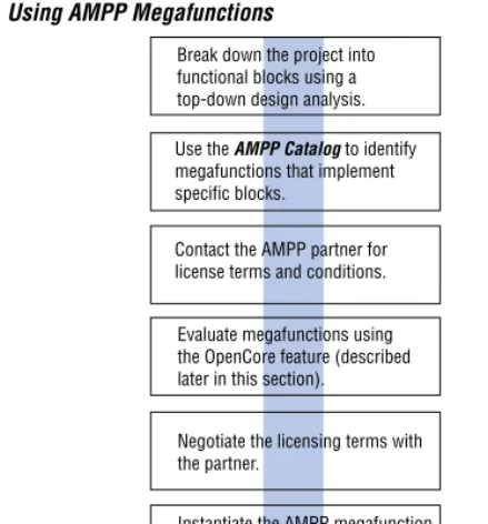
Figure 1 illustrates the typical process for evaluating, licensing, and using AMPP megafunctions.
Figure 1. Using AMPP Megafunctions
AMPP megafunctions can also be programmed and/or customized.
Programmable megafunctions can be configured “on-the-fly,” which changes behavior or specific function settings (e.g., a shift register with a dynamically adjustable maximum depth). Customizable megafunctions are modified by AMPP partners to create new versions. Megafunctions that are customized may be included in the quoted license fee, but are typically subject to additional modification or consulting fees.
Use the AMPP Catalog to identify megafunctions that implement specific blocks.
Contact the AMPP partner for license terms and conditions.
Instantiate the AMPP megafunction in the project hierarchy and compile the design.
Break down the project into functional blocks using a top-down design analysis.
Evaluate megafunctions using the OpenCore feature (described later in this section).
Negotiate the licensing terms with the partner.
Simulate the design.
Generate the programming files and perform hardware verification.
Altera Corporation 3 Introduction
Bus
2
Interfaces
Parameterized Megafunctions via MegaWizard Plug-Ins
Altera is the first PLD vendor to offer customers the capability to alter key megafunction parameters without restricting the end user’s design flow.
MegaWizard™ Plug-Ins allow users to customize megafunctions to meet specific design objectives, greatly reducing the time spent specifying a custom function. Because MegaWizard Plug-Ins are a recent innovation, AMPP partners are still in the process of creating plug-ins for many of their megafunctions; check with the AMPP partner directly for availability.
Available Formats
All AMPP megafunctions are available in post-synthesis Altera Hardware Description Language (AHDL) format, a fully minimized and optimized netlist that can be used without risk of changes during design processing.
Although VHDL and Verilog HDL files are available from most partners, a source code license is usually more expensive than a post-synthesis netlist license because the source code versions represent more intrinsic value.
Altera recommends using post-synthesis netlists to avoid synthesis variation issues during design processing. This process ensures that engineering effort is not required to reoptimize the behavioral source code.
OpenCore Feature
Altera’s MAX+PLUS® II software provides the OpenCore™ feature, which allows designers to evaluate megafunctions prior to licensing. The OpenCore feature allows designers to compile a megafunction and determine its size and speed, but it prevents the designer from generating programming or configuration files. This feature allows AMPP partners to offer OpenCore evaluations without risking their licensing interests.
To receive an OpenCore version of a specific megafunction, contact the AMPP partner directly for an authorization code; the AMPP partner will generate this code based on your MAX+PLUS II PC or UNIX workstation identification.
OpenCoreTM
Introduction
Megafunctions in the Design Flow
AMPP megafunctions are intended as “drop-in” design elements for all design flows supported by the MAX+PLUS II software. Although the megafunctions are developed as stand-alone functions, they can be integrated with other megafunctions and logic in a top-down design methodology. The ideal design flow assesses a project’s functional block requirements and assigns megafunctions to implement different portions of a system. Once the megafunction blocks are defined, designers can focus on design elements that are proprietary or cannot be implemented with megafunctions. For design flows that use only the MAX+PLUS II software, the designer can use the megafunction in a Graphic Design File (.gdf), AHDL Text Design File (.tdf), Verilog Design File (.v), or VHDL Design File (.vhd).
AMPP megafunction support extends to third-party design flows that are currently supported by Altera tools. For design flows that use standard EDA tools in addition to the MAX+PLUS II software, designers can instantiate AMPP megafunctions in a design by specifying the cell and port names in an HDL design file. During design processing, the EDA tool will pass the megafunction’s cell and port names into the EDIF netlist file. The EDA tool does not process beyond the name level during compilation; the MAX+PLUS II software replaces the cell name with the actual functional specification. Once the megafunction is part of a MAX+PLUS II project hierarchy, the designer must specify three synthesis options before the megafunction can be processed by the MAX+PLUS II software:
■ Assign the megafunction to a clique, which ensures that the placement of the megafunction is optimized for high performance.
■ Assign the WYSIWYG logic synthesis style, which instructs the MAX+PLUS II software to turn off logic synthesis when it processes the megafunction.
■ Apply any top-level timing assignments provided by the AMPP partner to the hierarchy before design processing.
f
For information on cliques, logic synthesis styles, and instantiating functions, go to MAX+PLUS II Help.During compilation, the MAX+PLUS II software recognizes the megafunction as an AMPP megafunction and verifies the megafunction license. The MAX+PLUS II software then completes design processing according to the permissions granted by the AMPP megafunction license.
Altera Corporation 5 Introduction
Bus
2
Interfaces
Performance & Density Specifications
The performance and density specifications in this catalog apply to megafunctions that are compiled as stand-alone designs. Additional logic synthesis may affect the performance or density of a megafunction, particularly when the function is combined with other megafunctions or logic. Megafunctions shipped as post-synthesis AHDL files have minimal performance or density variations, because additional design processing is not required. Megafunctions supplied as behavioral source code files may change in performance or density, depending on the design and the target device. Timing cannot be determined until synthesis and place and route of the final design is complete.
Each AMPP megafunction has a performance metric that provides performance information when the megafunction is compiled as a stand- alone project. The metric is usually a global clock speed or fMAX, but in some cases, other metrics such as a propagation delay or
samples/second is given. The global clock setup time (tSU) and global clock-to-output (tCO) delay are also useful parameters. Contact the AMPP partner to determine which additional performance metrics are available for the megafunction.
In general, a global clock frequency is not affected by the I/O delays that route the signal off-chip, whereas the tSU and tCO parameters are directly affected by on-chip and off-chip routing. If a megafunction is integrated with other logic or megafunctions on the same device, the set-up and clock-to-output delays are reduced because off-chip/on-chip delays are not required.
1 Subsequent versions of the MAX+PLUS II software,
megafunction design modifications, or the availability of faster speed-grade devices may affect density or performance characteristics. Contact the AMPP partners for the latest megafunction specifications.
Introduction
AMPP Megafunction Package Contents
An AMPP megafunction package typically contains the following items (items that accompany every package are highlighted in blue):
■ Megafunction license
■ Megafunction design file (typically a post-synthesis netlist)
■ Symbol File (.sym) for use in MAX+PLUS II GDFs
■ Include File (.inc) for use in MAX+PLUS II TDFs
■ VHDL and Verilog HDL instantiation templates
■ Megafunction documentation
■ Top-level timing assignments
■ Help file (typically in HTML)
■ Simulation stimulus file(s)
AMPP partners provide different levels of support and documentation.
Designers should contact the AMPP partner directly to ensure that appropriate support is provided. Most partners will supply sophisticated simulation information, such as pre-synthesis bus simulation models for use in third-party logic synthesis tools prior to processing in the MAX+PLUS II software.
Licensing AMPP Megafunctions
AMPP megafunctions are licensed directly from AMPP partners. The terms and conditions of each AMPP megafunction license may vary from partner to partner. Each AMPP partner typically specifies the
megafunction licensing terms based on the needs of the end user. AMPP megafunction license options may include:
■ Duration of the license (e.g., lifetime, 1 year, or 6 months)
■ Source-code access
■ OpenCore feature
AMPP megafunction licenses are generally limited to Altera PLDs. You should receive written permission before targeting an AMPP
megafunction for a non-Altera PLD (e.g., a gate array). Such use of an AMPP megafunction may require an additional license and/or payment to the AMPP partner.
The duration of an AMPP megafunction license typically defines the period of time during which the AMPP megafunction may be compiled as part of a MAX+PLUS II project. Once the programming file for an Altera PLD has been created, AMPP megafunction licenses generally convey unlimited lifetime manufacturing rights. Limitations in the use of
Altera Corporation 7 Introduction
Bus
2
Interfaces
To protect the embedded IP, AMPP megafunctions are typically shipped as encrypted files. Although the megafunction design file has a standard filename (e.g., function.tdf), the file appears corrupted when opened with a text editor. The encrypted megafunction design file is actually a binary file. Authorization and decryption are handled by the MAX+PLUS II software, using a megafunction authorization code that is generated and supplied by the AMPP partner.
AMPP megafunction licenses use the same authorization process as the MAX+PLUS II software. The MAX+PLUS II software for PCs uses an embedded license system, based on the serial number of the
MAX+PLUS II software guard (guard ID). UNIX workstation versions of the MAX+PLUS II software use the FLEXlm license manager and treat each AMPP megafunction as a new MAX+PLUS II feature. UNIX workstation licensing can either be locked or floating node, depending on the licensing partner’s policy.
AMPP megafunction licenses are supplied by individual AMPP partners, not by Altera. Altera cannot generate licenses for AMPP megafunctions.
AMPP
Megafunction Pricing
Designers should contact the appropriate AMPP partner for a quote or estimate of a megafunction license. To help determine the cost of a megafunction license and to ensure that the megafunction successfully integrates with the end application, be prepared to provide the AMPP partner the following information:
■ Relevant megafunction parameters (e.g., bus width, resolution)
■ License duration requirements (e.g., lifetime, 6 months)
■ Target device architecture (e.g., FLEX® 10K, MAX® 9000 devices)
■ Netlist-only or source-code license
■ Any requirements for modifications or feature changes
■ Any requirements for design migration (e.g., to an ASIC)
Technical Support
AMPP megafunctions are carefully developed by AMPP partners to ensure the highest possible quality. If a problem is traced to a
megafunction, the AMPP partner is responsible for resolving the problem.
If a problem arises with integrating the megafunction with other logic, Altera will provide appropriate engineering support.
Warranty
The megafunctions in this catalog, as well as other megafunctions and services available from the AMPP partners, are provided without warranty by Altera. Altera expressly disclaims all warranties, express and implied, with respect to the megafunctions supplied by the AMPP partners, including, but not limited to, implied warranties of merchantability, fitness for a particular purpose, title and non- infringement.Introduction
The AMPP partners may offer guarantees or warranties for design performance or functionality; contact individual AMPP partners for details.
®
Altera Corporation 9
Bus & Interface
June 1998
Overview
Implementing a bus interface function that meets design specifications is a challenging task that requires considerable design expertise. Altera Megafunction Partners Program (AMPPSM) partners offer pre-synthesized and pre-verified solutions for standard serial and parallel buses. Using AMPP megafunctions can shorten the development cycle dramatically, not only during the design entry phase using the OpenCore™ feature, but also during the simulation phase with hardware-proven solutions and testbenches. AMPP partners also have the expertise to provide drivers for complex bus protocols such as peripheral component interconnect (PCI), FireWire, and universal serial bus (USB).Contents
The bus and interface section contains the following functions:Parallel Bus
32-Bit PCI Target ...10, 12 32-Bit PCI Master/Target ...14, 16 64-Bit PCI Target ...18, 20 64-Bit PCI Master/Target ...22, 24
IEEE 1284 Parallel Slave Interface ...27
PCI Host Bridge...29
PowerPC Bus Master ...31
PowerPC Bus Slave...33
Serial Bus
CAN Bus...35IEEE 1394 Link Layer Controller ...37, 38 IIC Master...40
IIC Slave...41
USB Function Controller...42, 44 USB Host Controller ...46, 48 USB Hub Controller...50
VUSB Embedded Host Controller...52
Bus & Interface
32-Bit PCI Target
Vendor: Eureka Technology Target Application:
All PCI-based systems Additional Deliverables:
Simulation files, test vectors, top-level design template, training
ID Code: 2107-A112
■ Fully compliant with peripheral component interconnect Special Interest Group’s (PCI-SIG) PCI Local Bus Specification,
Revision 2.1
■ Supports zero-wait state burst mode data transfer
■ Internal write buffer to maximize data bandwidth
■ Optional first-in first-out (FIFO) interface
■ 33-MHz operating frequency
General Description
The 32-bit PCI target megafunction provides a user-friendly interface between a target device and a PCI bus. This megafunction is a very compact design that minimizes logic cell count while providing a high-bandwidth data transfer. The megafunction performs all data transfer functions requested by the PCI bus master. To maximize data bandwidth, the megafunction provides an internal write buffer and supports burst mode data transfer. All PCI configuration requests are processed locally by the megafunction.
Modifiable Parameters
The megafunction is available in Altera Hardware Description Language (AHDL), Verilog HDL, VHDL, and netlist format. Eureka Technology can customize the megafunction to meet user requirements. Contact Eureka Technology or visit their web site for more information.
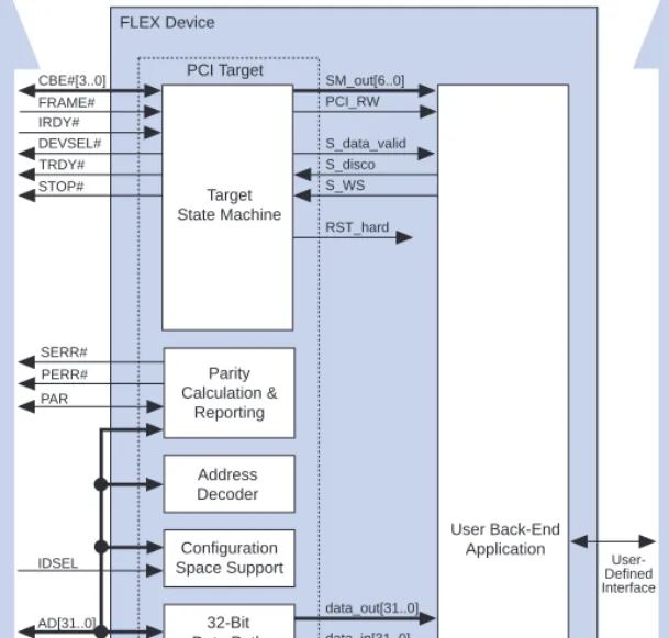
Block Diagram
Figure 1 shows the block diagram for the 32-bit PCI target megafunction.
Altera Corporation 11 Bus & Interface
Bus
2
Interfaces
Figure 1. 32-Bit PCI Target Megafunction Block Diagram
Device Utilization Examples
Device Speed
Grade
Utilization Performance Parameter Settings Logic Cells EABs
EPF10K10 -3 310 0 33 MHz Non-burst target design
EPF6016 -2 310 – 33 MHz Non-burst target design
Peripheral Device
User Bus
PCI Bus 32-Bit PCI Target
Address
Write Buffer
Configuration Registers Control Logic
Read Buffer
Bus & Interface
32-Bit PCI Target
Vendor: PLD Applications Target Application:
Digital signal processing (DSP), high-speed data transfer, bus migration, technology migration Additional Deliverables:
Simulation file, constraint file, development board, user guide, reference design ID Code: 73E2-1104
■ 32-bit, 33-MHz PCI function
■ Fully compliant with PCI-SIG PCI Local Bus Specification, Revision 2.1
■ Optimized for the Altera FLEX® 10K and FLEX 6000 device architectures
■ Fully synchronous design
■ Tested on hardware
■ Supports full-speed burst up to 132 Mbytes/second
■ Provides zero-wait state data transfers
■ Medium-speed decoder
■ Fully customizable function
■ Support for two base address registers (BARs)
■ Zero pre-placed or pre-routed logic
■ 3 to 5 minute compilation time
General Description
The 32-bit PCI target megafunction is a 32-bit, 33-MHz PCI bus interface that is used for high-speed data transfer applications.
This megafunction provides a simple and flexible interface between the PCI bus and a user-developed back-end design. The megafunction comes with a set of AHDL and VHDL back-end reference designs that designers can customize for their own project. These reference designs include interfaces that use FLEX 10K embedded array blocks (EABs) as synchronous SRAM buffers or FIFO buffers. Another back-end design provides an interface to an external SRAM buffer.
In addition to the required target features, the megafunction handles one interrupt line, supports fast back-to-back accesses, and implements a 32-bit user-configurable generic I/O port. The megafunction can still be customized to support additional user-specified features (e.g., multiple BARs and additional user I/O ports).
This 32-bit PCI target megafunction has been extensively simulated and tested on hardware using PLD Applications’ commercialized
PCI_GEN02 (FLEX 10K-based) and PCI_GEN6K (FLEX 6000-based) PCI prototyping boards.
Block Diagram
Altera Corporation 13 Bus & Interface
Bus
2
Interfaces
Figure 2. 32-Bit PCI Target Megafunction Block Diagram
Device Utilization Examples
Device Speed
Grade
Utilization Performance Parameter Setting Logic Cells EABs
EPF10K50V -2 347 0 60 MHz Contact PLD Applications
EPF10K30 -1 347 0 91 MHz Contact PLD Applications
-3 347 0 40 MHz Contact PLD Applications
EPF6016 -2 356 – 46 MHz Contact PLD Applications
PCI Target CBE#[3..0]
FRAME#
IRDY#
DEVSEL#
TRDY#
STOP#
SERR#
PERR#
PAR
IDSEL
AD[31..0]
INTA#
SM_out[6..0]
PCI_RW S_data_valid S_disco S_WS RST_hard
data_out[31..0]
data_in[31..0]
COM_in0 COM_out0 COM_out1 COM_in[m..1]
COM_out[n..2]
User- Defined Interface
PCI Bus Local Bus
FLEX Device
Target State Machine
User Back-End Application Parity
Calculation &
Reporting
Address Decoder
Configuration Space Support
32-Bit Data Path
Interrupt Support User I/O Communication
Bus & Interface
32-Bit PCI Master/Target
Vendor: Eureka Technology Target Application:
All PCI-based systems Additional Deliverables:
Simulation files, test vectors, top-level design template, training
ID Code: 2107-B040
■ Fully compliant with PCI-SIG PCI Local Bus Specification, Revision 2.1
■ Supports zero-wait state burst data transfer
■ Provides bus initiator and target capability
■ 33-MHz operating frequency
General Description
The 32-bit PCI master/target megafunction is a flexible interface between a bus master device, such as a direct memory access (DMA) controller or video coprocessor, and the PCI bus. The megafunction supports high bandwidth data transfer up to 133 Mbytes/second. All PCI configuration registers are included in the megafunction, and configuration requests are processed locally by the megafunction.
This megafunction also includes PCI target capability, which is useful for transferring data as a target and for setting up the control register of a bus mastering device.
The megafunction is available in AHDL, Verilog HDL, VHDL, and netlist format.
Modifiable Parameters
Eureka Technology can customize the design according to specific user requirements. Contact Eureka Technology or visit their web site for more information.
Block Diagram
Figure 3 shows the block diagram for the 32-bit PCI master/target megafunction.
Altera Corporation 15 Bus & Interface
Bus
2
Interfaces
Figure 3. 32-Bit PCI Master/Target Megafunction Block Diagram
Device Utilization Examples
Device Speed
Grade
Utilization Performance Parameter Setting Logic Cells EABs
EFP10K10 -3 650 0 33 MHz Contact Eureka Technology
EPF6016 -2 650 – 33 MHz Contact Eureka Technology
32-Bit PCI Master/Target
Target Controller
Write Buffer
Address Buffer
Parity Address-In Bus
Control Bus
PCI Bus Address Signals
PCI Bus Control Signals
Address-Out Bus
Write Buffer Configuration
Registers
Master Controller
Back-End Device PCI Bus
Bus & Interface
32-Bit PCI Master/Target
Vendor: PLD Applications Target Application:
DSP, high-speed data transfer, bus migration, technology migration Additional Deliverables:
Simulation file, constraint file, development board, user guide, reference design ID Code: 73E2-1204
■ 32-bit, 33-MHz PCI function
■ Fully compliant with PCI-SIG PCI Local Bus Specification, Revision 2.1
■ Optimized for the Altera FLEX 10K and FLEX 6000 device architectures
■ Fully synchronous design
■ Tested on hardware
■ Supports full-speed burst up to 132 Mbytes/second as initiator or target
■ Provides zero-wait state data transfers as a master or target
■ Automatic reiteration of interrupted transactions
■ Supports a dual-mode DMA engine accessible from the PCI side and from the local side
■ Medium-speed decoder as a target
■ Fully customizable function
General Description
The 32-bit PCI master/target megafunction is a 32-bit, 33-MHz PCI bus interface that is used for high-speed data transfers and real-time computing applications. This megafunction provides a simple and flexible interface between the PCI bus and a user-developed back-end design. The megafunction comes with a set of AHDL and VHDL back- end reference designs that designers can customize for their own project.
These reference designs include interfaces that use FLEX 10K EABs as synchronous SRAM buffers or FIFO buffers. Another back-end design provides the interface to an external SRAM buffer.
The 32-bit PCI master/target megafunction is fully parameterizable. In addition to the required master and target features, the megafunction handles one interrupt line, supports fast back-to-back accesses as a target, and implements a 32-bit user-configurable generic I/O port. It also supports all types of master and target transaction terminations, and automatically reiterates interrupted transactions when allowed. The megafunction can still be customized to support specific features (e.g., multiple BARs, additional user I/O ports, additional DMA channels, and optional master features). The megafunction has been extensively simulated and tested on hardware, using PLD Applications’
commercialized PCI_GEN02 (FLEX 10K-based) and PCI_GEN6K (FLEX 6000-based) PCI prototyping cards.
Altera Corporation 17 Bus & Interface
Bus
2
Interfaces
Figure 4. 32-Bit PCI Master/Target Megafunction Block Diagram
Device Utilization Examples
Device Speed
Grade
Utilization Performance Parameter Setting Logic Cells EABs
EPF10K50V -2 812 0 49 MHz Contact PLD Applications
EPF10K30 -1 812 0 75 MHz Contact PLD Applications
-3 812 0 35 MHz Contact PLD Applications
EPF10K20 -3 812 0 39 MHz Contact PLD Applications
EPF6016 -2 821 – 37 MHz Contact PLD Applications
PCI Master/Target CBE#[3..0]
FRAME#
IRDY#
DEVSEL#
TRDY#
STOP#
REQ#
SERR#
GNT#
PERR#
PAR
IDSEL
AD[31..0]
INTA#
SM_out[9..0]
PCI_RWn M_data_valid S_data_valid S_disco S_WS M_access M_hold M_gnt M_end M_abort T_abort
RST_pci CLD_pci
M_en
data_out[31..0]
data_in[31..0]
COM_in0 COM_out0 COM_out1 COM_in[n..1]
COM_out[n..2]
M_reg M_reg[1..0]
M_reg_cs M_reg_in[31..0]
DMA_cout[31..0]
User- Defined Interface
PCI Bus Local Bus
Master/Target State Machine
User Back-End Application Parity
Calculation &
Reporting
Address Decoder Configuration Space Support
32-Bit Data Path
Interrupt Support User I/O Communication
DMA Support
Bus & Interface
64-Bit PCI Target
Vendor: Eureka Technology Target Application:
All PCI-based systems Additional Deliverables:
Simulation files, test vectors, top-level design template, training
ID Code: 2107-C42A
■ Fully compliant with PCI-SIG PCI Local Bus Specification, Revision 2.1
■ 64-bit PCI bus
■ Zero-wait state burst data transfer with internal write buffer
■ 33-MHz operating frequency
General Description
The 64-bit PCI target megafunction is designed for interfacing user logic with a 64-bit PCI bus. This megafunction is a very compact design that minimizes logic cell count while offering double the bandwidth performance of a 64-bit bus system.
An internal write buffer is included in this design to support zero-wait state burst transfer and a very long burst length. The megafunction can transfer data up to 266 Mbytes/second. Both 64-bit and 32-bit data transfer rates are supported by this megafunction. All compliant configuration registers are included in the megafunction and all configuration accesses are processed automatically.
The megafunction is available in AHDL, Verilog HDL, VHDL, and netlist format. Megafunction sizes vary with features and customization.
Contact Eureka Technology for a logic cell count that is based on user specifications.
Modifiable Parameters
Eureka Technology can customize the design according to specific user requirements. Contact Eureka Technology or visit their web site for more information.
Block Diagram
Figure 6 shows the block diagram for the 64-bit PCI target megafunction.
Altera Corporation 19 Bus & Interface
Bus
2
Interfaces
Figure 5. 64-Bit PCI Target Megafunction Block Diagram
Device Utilization Examples
Device Speed
Grade
Utilization Performance Parameter Settings Logic Cells EABs
EPF10K30 -3 500 0 33 MHz Contact Eureka Technology
EPF6016 -2 500 – 33 MHz Contact Eureka Technology
Peripheral Device
User Bus
PCI Bus 64-Bit PCI Target
Address
Write Buffer
Configuration Registers Control Logic
Read Buffer
Bus & Interface
64-Bit PCI Target
Vendor: PLD Applications Target Application:
DSP, high-speed data transfer applications, bus migration, technology migration Additional Deliverables:
Simulation file, constraint file, development board, user guide, reference design ID Code: 73E2-1164
■ 64-bit, 33-MHz PCI function
■ Fully compliant with PCI-SIG PCI Local Bus Specification, Revision 2.1
■ Optimized for the Altera FLEX 10K and FLEX 6000 device architectures
■ Fully synchronous design
■ Tested on hardware
■ Supports full-speed burst up to 266 Mbytes/second
■ Provides zero-wait state data transfers
■ Medium-speed decoder
■ Fully customizable function
■ Zero pre-routed or pre-placed logic
■ 5-minute typical compilation time
General Description
The 64-bit PCI target megafunction extends the 32-bit PCI target megafunction data path to 64 bits. The megafunction is intended for applications with a 64-bit data path capable of supporting burst transfers up to 266 Mbytes/second.
The 64-bit PCI target megafunction maintains the functionality of the 32-bit PCI target megafunction. In addition, the back-end application can enable/disable support for 64 bits. When 64-bit support is enabled, the megafunction indicates to back-end applications the nature of the transfer (i.e., 32 or 64 bits). When 64-bit support is disabled, the megafunction behaves exactly like the 32-bit version.
Modifiable Parameters
The following megafunction parameters can be modified:
Modifiable Parameters (Part 1 of 2)
Parameter Description
VENDOR_ID Vendor identification DEVICE_ID Device identifier REVISION_ID Revision number CLASS_CODE Class code identifier
Altera Corporation 21 Bus & Interface
Bus
2
Interfaces
SPACE_SIZE Device memory space size MEM_LOCATE Device memory space location COM_IN User-configurable input port size COM_OUT User-configurable output port size Device Utilization Examples
Device Speed
Grade
Utilization Performance Parameter Settings Logic Cells EABs
EPF10K50V -1 440 0 63 MHz Contact PLD Applications
EPF10K30 -1 440 0 98 MHz Contact PLD Applications
-3 440 0 39 MHz Contact PLD Applications
EPF10K20 -3 440 0 49 MHz Contact PLD Applications
EPF6024 -2 440 – 63 MHz Contact PLD Applications
EPF6016 -2 440 – 49 MHz Contact PLD Applications
Modifiable Parameters (Part 2 of 2)
Parameter Description
Bus & Interface
64-Bit PCI Master/Target
Vendor: Eureka Technology Target Application:
All PCI-based systems Additional Deliverables:
Simulation files, test vectors, top-level design template, training
ID Code: 2107-C061
■ Fully compliant with PCI-SIG PCI Local Bus Specification, Revision 2.1
■ 64-bit PCI bus
■ Zero-wait state burst data transfer
■ Includes both bus master and bus target functions
General Description
The 64-bit PCI bus master/target megafunction interfaces bus mastering devices, such as DMA controllers or video coprocessors, to the PCI bus.
It processes all data requests from the bus mastering device and translates them into PCI bus requests.
This megafunction is designed for a 64-bit PCI bus system, which doubles the data bandwidth of a 32-bit PCI system. It supports zero-wait state burst transfers and a very long burst length. The megafunction supports up to a 266 Mbytes/second data transfer rate, and both 64-bit and 32-bit data transfers.
The 64-bit PCI master/target megafunction contains the functions of a bus master and a bus target. The device data and status can be accessed as a PCI master or target. All compliant configuration registers are included in the megafunction and all configuration accesses are processed automatically. This megafunction is available in AHDL, Verilog HDL, VHDL, and netlist format.
Modifiable Parameters
Eureka Technology can customize the design according to specific user requirements.
Block Diagram
Figure 6 shows the block diagram for the 64-bit PCI bus master/target megafunction.
Altera Corporation 23 Bus & Interface
Bus
2
Interfaces
Figure 6. 64-Bit PCI Master/Target Megafunction Block Diagram
Device Utilization Examples
Device Speed
Grade
Utilization Performance Parameter Settings Logic Cells EABs
EPF10K30 -2 1,050 0 33 MHz Contact Eureka Technology
EPF6016 -3 1,050 – 33 MHz Contact Eureka Technology
64-Bit PCI Master/Target
Target Controller
Write Buffer
Address Buffer
Parity Address-In Bus
Control Bus
PCI Bus Address Signals
PCI Bus Control Signals
Address-Out Bus
Write Buffer Configuration
Registers
Master Controller
Back-End Device PCI Bus
64-Bit PCI Master/Target
Vendor: PLD Applications Target Application:
DSP, high-speed data transfer, bus migration, technology migration Additional Deliverables:
Simulation file, constraint file, development board, user guide, reference design ID Code: 73E2-1264
■ 64-bit, 33-MHz function
■ Fully compliant with PCI-SIG PCI Local Bus Specification, Revision 2.1
■ Optimized for the FLEX 10K and FLEX 6000 device architectures
■ Fully synchronous design
■ Tested in hardware
■ Supports full-speed burst up to 266 Mbytes/second as initiator or target
■ Provides zero-wait state data transfers as an initiator or target
■ Automatic reiteration of interrupted transactions
■ Supports a dual-mode DMA engine accessible from the PCI side and from the local side
■ Medium-speed decoder as a target
■ Fully customizable megafunction
General Description
The 64-bit PCI master/target megafunction extends the 32-bit PCI master/target megafunction data path to 64 bits. The megafunction is intended for applications with a 64-bit data path capable of supporting burst transfers up to 266 Mbytes/second.
The 64-bit PCI master/target megafunction maintains the functionality of the 32-bit PCI master/target megafunction. In addition, the back-end application can enable or disable the support for 64 bits. When 64-bit support is enabled, the megafunction indicates to the back-end application whether the data transfer is 32 bits or 64 bits. When 64-bit support is disabled, the megafunction behaves exactly like the 32-bit version.
Altera Corporation 25
Bus
2
Interfaces
Modifiable Parameters
The following megafunction parameters can be modified:
Block Diagram
Figure 7 shows the block diagram for the 64-bit PCI master/target megafunction.
Modifiable Parameters
Parameter Description
VENDOR_ID Vendor identifier DEVICE_ID Device identifier REVISION_ID Revision number CLASS_CODE Class code identifier MIN_GNT Minimum grant time MAX_LATENCY Maximum latency time PREFETCH Memory attributes SERR_ENABLE SERR# control
SPACE_TYPE Device memory space type (I/O or MEM) SPACE_SIZE Device memory space size
MEM_LOCATE Device memory space location COM_IN User configurable input port size COM_OUT User configurable output port size STATISTIC_REG Optional statistic register
Figure 7. 64-Bit PCI Master/Target Megafunction Block Diagram
Device Utilization Examples
Device Speed
Grade
Utilization Performance Parameter Setting Logic Cells EABs
EPF10K50V -2 915 0 44 MHz Contact PLD Applications
EPF10K30A -1 915 0 62 MHz Contact PLD Applications
EPF10K30 -3 915 0 35 MHz Contact PLD Applications
PCI Master/Target
CBE#[7..0]
FRAME#
IRDY#
DEVSEL#
TRDY#
STOP#
REQ#
SERR#
GNT#
PERR#
PAR64
IDSEL
AD[63..0]
INTA#
SM_out[9..0]
PCI_RWn M_data_valid S_data_valid S_disco S_WS M_access M_hold M_gnt M_end M_abort T_abort
RST_pci CLK_pci
M_en
data_out[63..0]
data_in[63..0]
COM_in0 COM_out0 COM_out1
COM_in[n..2]
COM_out[n..2]
M_reg M_reg[1..0]
M_reg_cs M_reg_in[31..0]
DMA_cout[31..0]
User- Defined Interface
PCI Bus Local Bus
S_64bit
S_BAR0
64bit_en ACK64#
REQ64#
PAR
Master/Target State Machine
User Back-End Application Parity
Calculation &
Reporting
Address Decoder
Configuration Space Support
32-Bit Data Path
Interrupt Support User I/O Communication
DMA Support
Altera Corporation 27
Bus
2
Interfaces
IEEE 1284 Parallel Slave Interface
Vendor: SIS Microelectronics Target Application:
Asynchronous parallel communications Additional Deliverables:
Simulation file ID Code: 7D0E-1284
■ Bidirectional interface between host computers and peripheral devices
■ Uses standard parallel port found on many computer systems
■ Fully tested, includes a complete test suite
■ Configurable for compatible mode timing of nACK and BUSY ports
■ Asserts interrupt or DMA requests when the transmit buffer is empty or the receive buffer contains data
General Description
The IEEE 1284 parallel slave interface megafunction is an interface for fully interlocked, asynchronous bidirectional parallel communications between host computers and peripherals. The megafunction is
compatible with the 8-bit IEEE 1284 and Centronics parallel port (printer) interfaces, and it can read data from and write data to the parallel printer port interface. It supports five operational modes: forward compatibility mode, extended capabilities port (ECP) mode with forward-only run- length encoding (RLE), ECP mode (forward and reverse), reverse nibble mode, and request device ID using nibble mode (reverse mode).
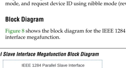
Block Diagram
Figure 8 shows the block diagram for the IEEE 1284 parallel slave interface megafunction.
Figure 8. IEEE 1284 Parallel Slave Interface Megafunction Block Diagram
Processor Interface
1284/Centronics Interface ioclk
n_Grst WrtEnb RdEnb dma_rd_wr n_iodmaack Addr[7..2]
Sdata[7..0]
n_SelectIn n_AutoFd n_Strobe n_Init Host_high CentDataI[7..0]
n_iodrq_reg n_ioirq
DataOut_1284[7..0]
n_fault Perror Select_xflag n_Ack Busy dir245 n_245_oe n_centdatadir_oe CentDataO[7..0]
IEEE 1284 Parallel Slave Interface
Device Utilization Examples
Device Speed
Grade
Utilization Performance Parameter Setting Logic Cells EABs
EPF10K30 -3 1,350 0 33 MHz Contact SIS Microelectronics
EPF6016 -2 910 – 27 MHz Contact SIS Microelectronics
Altera Corporation 29
Bus
2
Interfaces
PCI Host Bridge
Vendor: Eureka Technology Target Application:
All PCI-based systems Additional Deliverables:
Simulation files, test vectors, top-level design template, training
ID Code: 1207-D410
■ Fully compliant with PCI-SIG PCI Local Bus Specification, Revision 2.1
■ Connects the host CPU to the PCI bus to initiate PCI data transfers
■ Supports zero-wait state burst data transfer
■ Initiates PCI configuration access
General Description
The PCI host bridge megafunction provides an interface between the host CPU and the PCI bus. It allows the host CPU to access target devices residing on the PCI bus. The megafunction initiates PCI data read and write transfers upon request from the CPU.
The host bridge megafunction contains the functions necessary to initiate PCI data transfers. In addition, the megafunction is capable of initiating PCI configuration accesses. Configuration cycles are used by the host CPU to set up all PCI devices and to obtain device status. The
megafunction supports both the standard configuration mechanism and user-specific configuration mechanisms.
The PCI host bridge megafunction is designed for very high bandwidth data transfer. Zero-wait state bursting and write buffering are supported.
The megafunction handles data retry and automatically restarts PCI access upon retry. The PCI host bridge megafunction interfaces with many different types of CPUs, including big endian and small endian machines (e.g., x86 and all CPUs from the PowerPC family, including the 60x, 740/50, and 860). Through a generic internal bus, the megafunction can interface with virtually any available CPU.
This megafunction is available in AHDL, Verilog HDL, VHDL, and netlist format. Megafunction sizes vary with customization and with feature changes. Contact Eureka Technology directly for a logic cell count that is based on user specifications.
Modifiable Parameters
Eureka Technology can customize the design according to specific user requirements. Contact Eureka Technology or visit their web site for more information.
Block Diagram
Figure 9 shows the block diagram for the PCI host bridge megafunction.
Figure 9. PCI Host Bridge Megafunction Block Diagram
Device Utilization Examples
Device Speed
Grade
Utilization Performance Parameter Setting Logic Cells EABs
EFP10K10 -3 500 0 33 MHz Contact Eureka Technology
EPF6016 -2 500 – 33 MHz Contact Eureka Technology
PCI Address
Signals Double Entry Write Buffer
for Zero Wait State Support
PCI Control Signals Host CPU
Host Bridge Controller Configuration
Generation
Data Out Data In
Control
Address Buffer
Parity Generation
Read Buffer
Altera Corporation 31
Bus
2
Interfaces
PowerPC Bus Master
Vendor: Eureka Technology Target Application:
All PCI-based systems Additional Deliverables:
Simulation files, test vectors, top-level design template, training
ID Code: 1207
■ Compatible with all PowerPC bus architectures
■ Interfaces with bus mastering or bus snooping devices such as DMA controllers
■ Supports address pipelining and separate address and data tenure
General Description
The PowerPC bus master megafunction is a bus master that executes bus transactions on the PowerPC host bus. A simple and efficient user interface allows the user logic to reside directly on the PowerPC bus for high-performance data transfer. Together with the PowerPC bus slave, PowerPC bus arbiter, and PCI host bridge megafunctions, this
megafunction provides the complete system core logic function of a PowerPC-based system.
To maximize system performance, the PowerPC bus master
megafunction supports advanced features of the PowerPC bus such as address pipelining, address retry, bus parking, and separate arbitration for the address and data buses. This megafunction also supports both single beat and burst data transfers, and it allows address pipelining with two outstanding memory accesses.
The megafunction is available in AHDL, Verilog HDL, VHDL, and netlist format. Megafunction sizes vary with customization and with feature changes. Contact Eureka Technology directly for a logic cell count that is based on user specifications.
Modifiable Parameters
Eureka Technology can customize the megafunction according to specific user requirements, such as adding pipelining or using either snoop-only or regular data transfer. Contact Eureka Technology or visit their web site for more information.
Block Diagram
Figure 10 shows the block diagram for the PowerPC bus master megafunction.
Figure 10. PowerPC Bus Master Megafunction Block Diagram
Device Utilization Examples
Device Speed
Grade
Utilization Performance Parameter Setting Logic Cells EABs
EFP10K10 -3 160 0 50 MHz 160: With snoop only and pipelining
320: With regular data transfer and pipelining
EPF6016 -2 160 – 50 MHz
EPM7128 -7 80 – 66 MHz Contact Eureka Technology
User Logic
PowerPC Bus Master
Back Bus PowerPC Bus
PowerPC
Arbiter
Slave Memory Device
Other Devices
Altera Corporation 33
Bus
2
Interfaces
PowerPC Bus Slave
Vendor: Eureka Technology Target Application:
All PCI-based systems Additional Deliverables:
Simulation files, test vectors, top-level design template, training
ID Code: 1207-0108
■ Compatible with all PowerPC bus architectures
■ Interfaces with SRAM, SBRAM, FLASH, and user local buses
■ Supports data bursting with standard asynchronous SRAM
■ Supports address pipelining and separate address and data tenure
General Description
The PowerPC bus slave megafunction is a multi-function interface between the PowerPC bus and user devices such as asynchronous SRAM, synchronous burst SRAM, FLASH, and user local buses.
Together with the PowerPC bus master, PowerPC bus arbiter, and PCI host bridge megafunctions, this megafunction provides the complete system core logic function of a PowerPC-based system.
To maximize system performance, the megafunction supports advanced features of the PowerPC bus such as address pipelining, address retry, bus parking, and separate arbitration for the address and data buses. The megafunction also supports both single beat and burst data transfer, and it allows address pipelining with two outstanding memory accesses.
The megafunction is available in AHDL, Verilog HDL, VHDL, and netlist format. Megafunction sizes vary with customization and feature changes. Contact Eureka Technology for a logic cell count that is based on user specifications.
Modifiable Parameters
Eureka Technology can customize the megafunction according to specific user requirements, such as 32- or 64-bit data, pipelining, type of back-end device, adren mapping, and amount of memory mapped by the slave. Contact Eureka Technology or visit their web site for more information.
Block Diagram
Figure 11 shows the block diagram for the PowerPC bus slave megafunction.
Figure 11. PowerPC Bus Slave Megafunction Block Diagram
.
Device Utilization Examples
Device Speed
Grade
Utilization Performance Parameter Setting Logic Cells EABs
EFP10K10 -3 170 0 50 MHz 32-bit data, pipelined, back-end burst, and two memory spaces
EPF6016 -2 170 – 50 MHz
PowerPC Bus Slave
User
Registers
DRAM FLASH
Sync SBRAM
Async SRAM PowerPC Host Bus
Altera Corporation 35
Bus
2
Interfaces
CAN Bus
Vendor: SICAN Microelectronics Target Application:
Automotive electronics, home automation, simple sensor/actuator systems Additional Deliverables:
Simulation file, user guide ID Code: 18CD-47A4
■ Compatible with CAN Specification, Revision 2.0B passive/active
■ Completely synchronous flipflop design
■ Self-test mode
■ Readable error counters
■ Data transfer rate up to 1 Mbit/second
■ Cycle frequency of 12 MHz
General Description
The Controller Area Network (CAN) bus megafunction fulfills all protocol functions according to CAN Specification, Revision 2.0B, including extended functionality (CAN Specification, Revision 2.0B active). The CAN bus megafunction incorporates all the features required by CAN Specification Revision 2.0, including error handling capabilities, stuff bit generation, cyclic redundancy code (CRC), and multiple sample points.
The CAN bus megafunction has a universal interface for connection to the receive and transmit buffers, allowing the megafunction to be optimized for specific applications. The megafunction does not contain receive or transmit buffers; these buffers must be implemented externally.
Modifiable Parameters
SICAN can customize the size of the data output on the back-end device.
Block Diagram
Figure 12 shows the block diagram for the CAN bus megafunction.
Figure 12. CAN Bus Megafunction Block Diagram
Device Utilization Example
Device Speed
Grade
Utilization Performance Parameter Settings Logic Cells EABs
EPF10K20 -3 720 0 12 MHz 8-bit data output
Transmit Logic
StuffReg[5..0]
Majority Decision
Comparator
Receive[7..0] Transmit[7..0]
Bit Timing Logic
Sample[2..0]
CRC[14..0]
Comparator
Receive Error Counter
Transmit Error Counter SAM
CAN Bus
Tx
REC TEC ErrPas BusOff
TxRqst Status TxSuc MesValid MesError
SaveData Rec/Tx
Addr.
TxData[7..0]
RecData[7..0]
Rx
BusMon
Protocol FSM
Altera Corporation 37
Bus
2
Interfaces
IEEE 1394 Link Layer Controller (LLC- I )
Vendor: SIS Microelectronics Target Application:
Home local-area network (LAN), asynchronous transfer mode (ATM) bridge, real-time multimedia, digital satellite system (DSS), set-top boxes
Additional Deliverables:
Simulation file, demonstration board ID Code: 7D0E-1394
■ Conforms to IEEE 1394-1995 standard for cable environments
■ IEEE 1394a standard support on IEEE approval
■ Generic 32-bit host bus interface
■ Optional asynchronous host clock/cable clock
■ Supports IEEE 1394-Annex J physical interface
General Description
The IEEE 1394-compatible LLC-I megafunction provides IEEE 1394 asynchronous packet link layer support between a controller implementing the IEEE 1394 transaction layer and an external device implementing the IEEE 1394 physical layer.
Block Diagram
Figure 13 shows the block diagram for the IEEE 1394-compatible LLC-I megafunction.
Figure 13. IEEE 1394-Compatible LLC-I Megafunction Block Diagram
Notes:
(1) This information is preliminary.
(2) Data on the Annex J interface is clocked at 49.152 MHz.
Device Utilization Example Note (1)
Device Speed
Grade
Utilization Performance Note (2)
Parameter Setting Logic Cells EABs
EPF10K100A -1 3,352 6 50 MHz Contact SIS Microelectronics
1394 Physical Layer Device Optionally Included in
FLEX 10K Device
FLEX 10K Device
Control
32-Bit Data phyctl[1..0]
phydat[3..0]
ireq sclk
IEEE Std.
1394 Cable Ports
Generic Host Interface Annex J Interface
LLC-I Customer-Designed
Host or Application-Specific
Hardware-Based Controller
32-Bit Data
IEEE 1394 Link Layer Controller
Vendor: Simple Silicon Target Application:
Home LAN, ATM bridge, real-time multimedia, DSS, set-top boxes
Additional Deliverables:
User manual, netlist core, behavioral testbench, test cases, evaluation kit, Verilog HDL source code
ID Code: A441-BE01
■ Compliant with IEEE 1394 Specification, Draft 8.0 Version 2
■ Supports both asynchronous and isochronous data transfer modes
■ Designed for 100 Mbytes per second (Mbps), 200 Mbps, and 400 Mbps bus speeds
■ Supports PCI/industry-standard architecture (ISA) interface
■ Includes transaction layer, node controller, and bus management facility
■ Provides physical layer (PHY) interface compliant with IEEE 1394 specification
■ Supports external FIFO and ROM interfaces
■ Includes testbench and test suites covering the functionality, protocol, and error conditions
General Description
The IEEE 1394 link layer controller megafunction is the hardware implementation of the link layer and hardware portions of the
transaction layer and node controller protocols. The megafunction sends and receives data by forming it into packets, adding headers, and generating and checking the CRCs. When the megafunction wants to send data, it tells the PHY to gain access to the serial bus. When the PHY has accessed the bus, the megafunction sends parallel data to the PHY for serialization transmission through the cable. As data is received by the PHY, it delivers and sends the data to its link. The link determines whether the data is meant for it by reading the address in the header. If it is, the data is accepted and stored appropriately. If not, the data is ignored. A PCI interface is also available with the megafunction.
Modifiable Parameters
The following megafunction parameters can be modified:
Modifiable Parameters
Parameter Description
MAX_SPEED Maximum speed can be 100 Mbps, 200 Mbps, or 400 Mbps.
DATA BUS WIDTH For link PHY interface. Data bus width can be 2, 4, or 8 bits.
Altera Corporation 39
Bus
2
Interfaces
Block Diagram
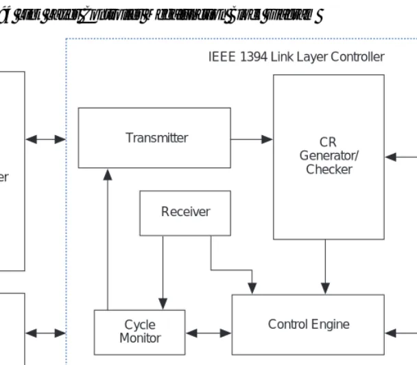
Figure 14 shows the block diagram for the IEEE 1394 link layer controller megafunction.
Figure 14. IEEE 1394 Link Layer Controller Megafunction Block Diagram
Notes:
(1) External FIFO buffers can be modeled as EABs, if needed.
(2) The megafunction is designed to support both isochronous and asynchronous modes. However, most applications require only one or the other. Choosing only one mode can result in over 30% savings in logic cell utilization.
Device Utilization Example Notes (1), (2)
Device Speed
Grade
Utilization Performance Parameter Setting Logic Cells EABs
EPF10K100 -3 4,296 0 50 MHz Contact Simple Silicon
PHY Interface TR
Handler
CSR &
Resource Manager
CR Generator/
Checker
<