MEMOIRS OF SHONAN ]NSTITUTE OF TECHNOIiOGY VoL 29.No. 1,1995
Interfaces
between
Ferroelectric
Ceramics
and
Superconducting
Oxide
SunaoSUGIHARA*
Superconducting oxide of YiBa2Cu307-.was pasted ina thickfilmon piezo electronic ceramics, Pb
(Zr,Ti)03
and theelectrical properties were evaluated from the temperatureof liq.N2 tothe roomtemperature. They showed the semiconductive property, although the resistivity was O,19・cm at 80
K without clear clitical temperature, Furthermore,Pb{Zr,Ti)03was sandwiched with YBCOs as the electrodes tomeasure piezoelectricityof thesystem.
The YiBa2Cu307..fi1rnthicknesses were determinedby scanning electron microscope
(SEM).
Anelectron probe microanalyzer(EPMA) revealed diffusionof Ba intoPb{Zr,Ti)03.The high density of
thick filmshould beachieved fornew composites with betterproperties.
1.
IntroductionInan electrode forceramics, wettability of a
metal on ceramics
is
of animportance
for
agood contact of them. A glassfritisemployed
for
joining
the metal with ceramics sincece-ramics does not generally bond with a metal.
Sugihara
et al.have
widely studied thewetta-bilityand bondability of rnetallceramics and
ceramicstceramics
for
the electronic ceramicsparticularly.i}・2)
Joining
of superconductor andsemiconduc-torwas theoreticallystudied on the
boundary
effects
by
P.
G.
De
Gennes,3)
in
whichsuper-conducting electrons migrate toward
semicon-ductor
by
the proximity effects. Theissue
isconcerned with a nanometer order, so called
mesoscopical.
There
have
been
several studiesof the proximity effect of superconductor.4)
The
Y-Ba-Cu-O
sy$tembased
multilayer foroptoelectronic
devices
wasinvestigated
on theR-plane sapphire and A1203 as IR detectors.5)
The
YBCO
films
werehundreds
of nm, andemployed
for
counterelectrode andbase.
In
the more rnacroscopical view point,Sriva-stava et at. reported YiBa2Cu307-. adhered
onto
BaTi03
andPb<Zr,Ti>03
(hereafter
PZT)
*
utsFx\ig
tztyrk
SPet 6
Hi
10n
12EftN
tocharacterize electrical properties of the
de-vices,6) Furthermore,
Moya
et al.formed
theYiBa2Cu307-x composites on
Ce-TZP,
Y-TZPand spinel substrate,T) The
interfaces
betweenYiBa2Cu307-.
{hereafter
YBCO)
and the otherceramics are very important toform the device
or the composite when one uses
YBCO
as anelectrode.
The firstpurpose isto
join
YBCO
thickfilm
with piezoelctronic ceramics, then to find
ap-propriate thickness and
better
contact of thefilm
togive good piezoelctricity andsupercon-ductivity.
The
second aimis
touse theYBCO
electrode
for
field
effect transistorat the lowtemperature, where the
film
works assemi-conductive rnaterial even
if
the temperaturefor
it's
operationis
notbelow
the transitiontemperature.
Furthermore,
an operation of anelectronic circuit at
lower
temperature willplay a role of ma・king the system rnore
accu-rate.
2. Experimental
1)
FabricationofPZT
The
PZT
powder whichthe
cornpositionis
Pb(Zro.s3,Tio,47)03has been supplied byFuji
Ti-tanium
Ind.
Co.
Ltd.
It
is
pressed at180MPa
followed
by
sinteringfor
2
hours
at 1503K.The
sintering was carried out in theShonan Institute of Technology
ShonanInstitute of Technology
vaM=*iFJit\$est
rg
29g
za
1g
sizes of sintered pelletswere 15mm
in
diame-terand
O.8-1.0mm
in
thickness.The
sintereddensity
was95-96%
tothe theoreticalone.2)
Slurry
ofYBCO
The YBCO powder supplied by
Seimi
Chem-ical
Co.,
Ltd.
was calcined at873K
was milledby Zr02 balls
(3
mm indiameter)for
24
hours
in
the
solvent.The
slurry was pasted on thePZT
fabricated
above, then sintered at1193
K
in
anoxygen atmosphere
(O.51itter/minJ
for
eachsintering tirne;5,60,420 minutes.
They
werecooled
down
to
a roomtemperature
at thespeed of about 1.5
Ktmin,
The
surface of thickfilmswere examined
by
X
raydiffraction
anal-ysis
(XRD).
3)
Interfaces
between
YBCO
and PZTThe
morphological analysis at theinterfaces
was carried out using scanning electron
micro-scope, and the element distributions through
the interfaceswere qualitatively
investigated
amapping with an eletron probe micro analyzer,
4) Electricalproperties
Electrical
resistivity was measured with afour-probe method from the temperature of
liquid N2 to a room temperature. YBCO/PZT/
YBCO
(SuperconductorllnsulatorlSupercon-ductor) was
investigated
for
frequency
depend-ence of the composite by the impedance
analy-zer
(YHP
4192A).
3.
ResultsandDiscussion
1)
Interfaces
of YBCO/PZT andYBCO
faces
Figures
1-a,
1-b
and 1-cshow theSEM
photo-graphs at the interfacesof
YBCO/PZT
systemsintered for 420, 60 and 5 minutes at
1193K,
respectively. The necking of
YBCO
grains areformed
although there seems tobe
porousin
the sintered YBCO thick
film
of 420 minutes.The
thickness of thefilm
was about17"m.
The
system maintained for 60 minutesin-dicated
very porous structure whichfilm
thickness was about
33ptm,
and the sinteredsystem of
5min
showedthe
densermorphol-ogy.
The
SEM
photographs on the surfaces ofa
b
cFig.
1. SEM photographs at the interfacesof
YBCOtPZT systems foreach sintering
time, a;420, b;60, c;5min,
the
YBCO/PZT
system are shownin
Fig.
2-a,
2-b and 2-c
for
the sintered specimens of 420,60
and 5min, respectively. As shown in Fig.2-a,
the well-developed neckings ofYBCO
gen-erated with porous microstructures on the 17 ptm-film sintered
for
420min.The
neckingsdid
not develop inthe filmwith thickness of about
33ptm
for
the sintered system of60min
asshown
in
Fig.
2-b
and seemed tobe
moreporous with thedifferentmicrostructures
from
thesintered systems of
5min
and420
min.It
is
not clear at
this
mDment why the sinteredsystem of
60min
shows thedifference
of themicrostructure. Inthe only sintered system of
5min,
thefilm
wasthinner
of 5pm and denser(Fig,
2-c),
and thinnerfilm
seems tobe
better
inteT:facesbetweenRerroelectricCeramicsand SmperconductingQxide
a
b
cFig.
2.SEM photographs on the surfaces in
YBCOiPZT systems for each sintering
time,a;420,b;60,c; 5min.
2)
Diffusion ofbarium
from YBCO to PZTY2BaCuOs and BaCu02 besides YBCO were
found
by
XRD
analysis when sintered for420minutes at
1193K,
andY2BaCuOs
of greencolour and non-superconducting materials
were
detected
withYBCO
peaksin
thesinteredfilm
of5
minutes.Figures
3-aand 3-bshow theEPMA
line
analysesindicating
the Badiffusion
distance
of35"m
and5um
into
thePZT
from
the interfaces,respectively.
The
length
ofBa
diffusionis
illustrated
inFig.4.3>
Electrical
resistivity and piezoelectricproperties
The resistivities were measured at the
tem-peratures
from
liq.
N2
to296K.
They
indicated
the serniconductive resistivities with
tempera-turedependences a$shown
in
Fig.
5.
However,
xl en=c-o a
2
1
Xlo31.2
u)avO,6bFig.
YBo
Coe'PZTO.070
mmo
O
O.070
mm3. EPMA line analysis at the interfaces
between YBCO and PZT ineach
ingtime,a;420,b;60,c; 5min.
theon-set temperature on 5"m
YBCO
filmwasnot clear although
O.1
9・cm
was shown at thetemperature of
80
K,and the resistivity at296
K
wasO.089・cm.
BaCu02 generatedin
thesintered system of
60min
wasnon-super-conductive materiaL More Ba and
Y
werede-tected on the surface of
YBCO
than in bulk,which cause was reported due to a large
amount of
C032-
ions.
Those elements and theesti-Shonan Institute of Technology ShonanInstitute of Technology
maMI*iFJi<#ept
n
29g
eg
1g
Z
503ka-40.!gts 30g-=.20
s.as
1.0 2.0 time , iog tFig.4. Change of Ba diffusion length in PZT
with sintering timeat 1193K.
iO.19qon-tsy.)D.1;-!ut
O,1yfi D.Iv.:c e.oem O.0 3A E oeVh -.-`22:m-eEt6',u-.V
Teinperature xlo2K
Fig. 5. Electricalresistivity changes with perature.
mated to reduce superconductivity.8}
The
piezoelectricity on the electrodes of 5"m thickness
YBCO
was measured.Absorp-tion
of energyby
PZT
coated withYBCO
thickfilm
was not much at thefrequency
around190
kHz according to
the
re$ultsby
impedance
ana-lysis
which meant the poor piezoelectricity.Ba
was
doped
at thedistance
of approximate16
"m
from
the surface ofPZT
so thattheeffect ofBa
could be estimated onthe
piezoelectricitieswith Ag electrodes.
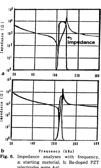
Figures
6-a
and6-b
showthe resonance and antiresonance absorptions
on t'hestandard PZT
(or
starting material) andAorvvv=qvmpt"H a le5 to4 ID3 o! oT oa
fiimpdance
leS -' lo4s: lo3s:cu loZHlol-Zl loO !abFig, 6. so ISO !31 3DOuo zEo 3sa figo
Frequency (kHz)
Impedance analyses with frequency,
a; starting material, b;Ba-doped PZT
(electrodes
were Ag),the Ba-doped PZT, respectively. At the
reso-nance
frequencies
around280kHz
for bothstandard
PZT
and Ba-doped one, the capaci-tancesincrease
indicating reversal peak sincefrequency
phase wasinverted,
and hence thereactances
(1/wC)
was nearly zero, as shownin
Fig.6-a and
6-b.
Electromechanical
couplingfactors
(Kp)
canbe
calculated by resonance and+antrresonance
frequencies. As shown inTable
1,Ba
did
not significantly seem to affect thepiezoelectricconstants such as
d3i
andg3i.
So
the film density and
Ba
diffusion
seem tocuase the poor piezoelectricityon the
YBCOt
PZTIYBCO system,
From
thesefacts,
it
is
sug-gested that the
density
ofYBCO
thick film isnot
high
enough as theelectrode ofYBCO
for
adevice
according to SEM analysis.The
causeof insuMcient
function
as the elctrodes ofinterft2cesbetween E2rroelectn'cCeramics and Smperconducting Oxide
Table 1Piezoelctric properties forstandard material and Ba-doped PZT.
kp dsi ×10-i2 gsl × 10-3 Er Frequency
(kHz)
resonance anti-reson, Standard PZT Ba-doped PZT O.57O.38 85.538,5 8.05,8 1215 752 281.6286.6 292.2304.0 le,;electro-mechanical coupling factor,d3i;piezoelectric(V・mtN), E,;relative permittivity,
constant(mtV}, g3]; piezoelectricoutput coeMcient
effect of
C032'
ions
in
the next step.
4.
Conclusions
The superconducting ceramics and
piezoel-ectric ceramics can be
joined
infilmand bulk,and
hence
theirfunctions willbe
possible forthe electrode and new
device.
1)
2)
3)
YBCO
thick films(5-33"m)
adhered ontoPZT,
The
investigation
of theinterfaces
revealed the diffusionof Ba from YBCO to
PZT,
and thelength
ofthe
diffusion
depen-ded on the sintering time at 1193K.
YBCO
thick filmof5"m
indicated rathersemiconductive properties than
supercon-ductivity
which critical temperature wasnot clear.
The thickfilmshould be denser tofunction
as the electrodes forthe composites of
sup-erconductortPZTIsuperconductor, and also
the film thickness of 5"m or
less
canbe
suggested as well as a short sintering time.
References
1}
S,
Sugihara and K. Okazaki,Proc.of
the 7thinternationatSym.
of
Appticationonics,pp. 429-431, June 6-9, 1993, Champaign, USA,
2) S.Sugihara and K. Okazaki,Proc.
of
the 7thinteTnationalSym,
of
APPIicationontn'cs,pp. 432-434,
June
6-9,1993, Champaign, USA,3) P. G. DeGenes, Rev. Mbd. Phys.,36, 225-237 (1965).
4> T. Nishino,E.Yamada and U.Kawabe, Phys.
Rev.B33,2042-2045
(1986),
5)
J,
C.Villegier,H,Moriceau, H.Boucher, L. Ciocio, A.Ghis, A.Jaeger,M. Levis,F.Pourtier, M.Schwerdtfeder,M.Vabre and C.Villard,MdtSci.,and Engi'neering,B15,92-100
(1992),
6> A, Srivatava,A.Bhallaand L.E.Cross,
electrics, 123,243-251
(1991).
7) E.Saiz,M.I,Osendi,P.Miranzo,
J.
Requena andJ.S.Moya,
f
Less-Comm. Mbtals,164 and 165,458-463
(1990).
8)