Research of High Efficiency and High Power
Density of Off-line Power Supplies
オフライン電源の高効率化及び高電力密度化
に関する研究
Dissertation for Doctor of Philosophy
in
Department of Electrical and Electronic Engineering,
University of Yamanashi
山梨大学大学院
医学工学総合教育部
博士課程学位論文
March 2017
2017 年 3 月
Jian Chen
陳
建
Abstract
In most recent electronics, such as computers, flat-panel TVs and LED lighting, off-line power supplies are used to convert AC power from the electrical grid (electric utilities) into DC power with isolation. This kind of off-line power supplies provide high conversion efficiency of energy and high power density thanks to the switching mode technologies. Generally, an off-line power supply with input power of no less than 75W consists of two-stage converters. First stage is an active boost PFC converter and the second one is a DC-DC converter with an isolation transformer.
As for the active boost PFC converters, the operation modes can be specified as: continuous conduction mode (CCM), critical conduction mode (CRM) and discontinuous conduction mode (DCM). Because the CCM boost PFC operates in average current mode with fixed switching frequency, it is easy to design the boost inductor and the EMI filter. Therefore, CCM boost PFC is a good choice in terms of power density by reducing the boost inductor and simplifying the EMI filter, especially the existence of SiC boost diodes. As for the isolated DC-DC converters, there are many kinds of topologies such as flyback, forward, resonant and phase shifted converters to meet the requirements of various applications. Compared with conventional flyback or forward off-line converters, LLC resonant converters are becoming more and more popular. It is because LLC resonant converters can achieve higher efficiency and higher power density thanks to the high voltage gain capability and the soft switching techniques such as so-called zero voltage switching (ZVS) and zero current switching (ZCS).
In this dissertation, the design challenges and solutions of the control technologies of the off-line converters with the CCM boost PFC converters and the isolated LLC resonant converters will be discussed. The objective of this dissertation is to achieve higher efficiency at light load conditions of the LLC resonant converters by realizing automatic burst control, and high density by simplifying the EMI filters, bulk capacitors and thermal design.
Many control technologies for the off-line power supplies with CCM boost PFC converters and LLC resonant converters are studied to meet the stricter requirements for
more efficient power delivery with smaller space. For example, spread spectrum techniques are studied to simplify the conducted EMI filters for CCM boost PFC converters, control techniques of anti-capacitive mode are researched to simplify the bulk capacitors and burst mode control techniques are provided to improve the conversion efficiency at light load conditions for LLC resonant converter.
However, many issues still remain for the mentioned control technologies.
As for the CCM boost PFC converters with conventional spread spectrum techniques, there is a trade-off relation between reduction in the volume of the EMI filters and high efficiency. A novel spread spectrum technique is presented to optimize both conducted EMI noise and conversion efficiency. A new analysis method is proposed with the 3rd
harmonic components of the boost inductor current ripple by Fourier Transform. The proposed method induces a saddle-type frequency modulation with maximum and minimum frequency limits. By the saddle-type frequency modulation, the improved conducted EMI performance is obtained without the sacrifice of the efficiency, resulting in a simplified conducted EMI filter experimentally. The analysis method can also be applied for the 2nd harmonic components of the boost inductor current ripple to meet
higher frequency applications of CCM boost PFC converters thanks to the existence of SiC boost diodes.
Regarding the LLC resonant off-line converters, the first issue is how to prevent capacitive mode without the peak gain impact, resulting smaller bulk capacitors and more robust LLC resonant off-line converters. A novel anti-capacitive mode technique is provided to improve the trade-off relation between the wide input voltage range and the protection of the half bridge switches like the power MOSFETs. A reliable detection method to avoid the capacitive mode is proposed by detecting the resonant current of the resonant capacitor and the resonant voltage of the primary side of the transformer. The input voltage range is optimized so that the bulk capacitor can be smaller to get higher power density for the LLC resonant off-line converters.
The second issue of the LLC resonant off-line converter is how to detect the load condition at the primary side accurately at the normal mode and burst mode.
than other PWM topologies at nominal load conditions, the efficiencies cannot be satisfied at light load conditions due to the magnetizing current. Therefore, burst mode control has been studied for the LLC resonant converters. On the other hand, in order to realize automatic burst mode control which is switching operation between normal mode and burst mode automatically, the control systems need to obtain load conditions accurately at both normal mode and burst mode. However, it is difficult for the LLC resonant off-line converters to detect the load conditions accurately without power loss at the primary side of the converters.
In this work, we propose and implement a lossless load detection technique for normal and burst mode by a novel average input current sensing method at the primary side of LLC resonant off-line converters. Detailed theoretical analysis at normal and burst mode is presented and a load detection circuit is proposed with the consideration of integrated circuits. To verify the analysis, an LLC resonant off-line converter with 400V input and 16V/10A output is simulated using PSIM and a prototype board is built. The experimental results show that the proposed load detection technique is valid and practical. As a result, an automatic burst mode control for LLC resonant converters at light load conditions is realized with the proposed average input current sensing method. At the same time, a precise overload protection is realized too to improve the thermal design, resulting higher power density.
Table of Contents
Chapter 1 Introduction
7
1.1 Background 7
1.2 Opportunities and challenges of CCM boost PFC converters 9 1.3 Opportunities and challenges of isolated LLC resonant
converters 11
1.4 Objectives and outline 15
References 17
Chapter 2 Spread spectrum method for CCM boost PFC
20
converters
2.1 Introduction of boost PFC converters 20
2.2 Analysis of 3rdharmonic component of inductor current 23
2.3 Analysis of spread spectrum method for simplifying 27 the EMI filter
2.4 Spread spectrum design of PFC control IC 30
2.5 Experimental results 32
2.6 Conclusion 36
References 37
Chapter 3 Control mothed for anti-capacitive mode of LLC
38
resonant converters
3.1 Introduction of LLC resonant topologies 38
3.2 Anti-capacitive mode technique 43
3.3 Optimization of the bulk capacitor 49
3.4 Conclusion 50
Chapter 4 Load detection technique of LLC resonant
52
converters
4.1 Improved LLC resonant converters 52
4.2 Analysis and design of load detection techniques 54
4.3 Simulation results 73
4.4 Experimental results of load detection 78
4.5 Application of automatic burst mode 81
4.6 Application of precise overload protection 83
4.7 Conclusion 88
References 89
Chapter 5 Conclusion and Future work
91
5.1 Conclusion 91
5.2 Future work 94
Papers on this research
95
Chapter 1
Introduction
This chapter presents the background, objectives and outlines of this dissertation. The challenges for off-line power supplies are described in terms of CCM boost PFC converters and LLC resonant converters respectively.
1.1 Background
Energy efficiency and renewable energy are said to be the twin pillars of sustainable energy policy to make deep cuts in fossil fuel use to reduce pollution [1]. In most recent electronics, such as computers, flat-panel TVs, LED lighting, off-line power supplies are used to convert AC power from electric utilities into DC power with high efficiency thanks to the switching mode technologies. The power supplies are designed to provide higher and higher efficiency conversion to meet the stricter energy efficiency requirements. The Energy Star program and the 80 PLUS are the representative standards of the requirements. For example, the Energy Star program defined the International
Efficiency Marking Protocol for External Power Supplies (EPS) [2]. Fig. 1-1 shows the efficiency requirements of marking level in terms of average efficiency minimums or average loss maximums measured at loading conditions of 100%, 75%, 50%, and 25% of the nominal load. The level six went into effect in the US in February, 2016. It is no doubt than the average efficiency requirements of over 90% will be met in the near future.
Additionally, the efficiency requirements at the light load condition of 10% of the nominal load may be considered by Energy Star program in the near future. It is because consumer products are increasingly spending a significant portion of their operating time in lower power modes where the EPS load-demand is below 25 percent [3].
At the same time, off-line power supplies manufactures are always managing to meet the continuous increasing power density requirements, so-called small space requirements. For example, the adapters of notebook PCs become smaller and smaller that are a competitive factor for notebook PCs.
An off-line converter is an electronic voltage regulation or current regulation device that is designed to provide direct current (DC) electric power from an alternating current (AC) utility power source. Fig. 1-2 shows a typical diagram of the off-line converters. The main component parts include EMI filters, active power factor correction (PFC) converters with continuous conduction mode (CCM), bulk capacitors and isolated dc-dc converters with LLC resonant topology, based on the interested research of this work.
1.2 Opportunities and challenges of CCM boost PFC converters
In applications of active PFC converters, it is popular to use the boost PFC converters as an economical solution to comply with the EN 61000-3-2 low frequency EMC standards [4].
Since the boost PFC converters are one kind of switched mode power supplies (SMPS) operating in high frequency range, it is almost necessary to use conducted EMI filters in compliance with the CISPR-22 standard [5]. According to the current of the boost inductor, the operation modes can be specified as: continuous conduction mode (CCM), critical conduction mode (CRM) and discontinuous conduction mode (DCM). Because CCM PFC operates in average current mode with fixed switching frequency, it is easy to design the boost inductor and the EMI filter thanks to the relatively small ripple current of the boost inductor. Therefore, CCM is a good choice in terms of power density [6], especially the existence of SiC diode [7].
According to the CISPR-22 standard, the limit of quasi-peak (QP) level starts at 66 dB with a roll-off of -20dB/decade during 150kHz to 500kHz as shown in Fig. 1-3.
On the other hand, the roll-off of the π type filter shown in Fig. 1-4 is -60dB/decade. It is clear that the farer away the 3rd harmonic component of the current ripple is from 150kHz, the better the effect of the EMI filter is [8].
The switching frequency (FSW) effect level of the EMI filter with comparison to
50kHz can be expressed as
k
F
dB
V
SW effect50
log
40
(1-1)For example, compared with the switching frequency with 50kHz, the 70kHz can obtain QP margin of 5.8dB.
However, higher switching frequency is coming up with higher switching loss, especially in the case of low input line voltage. It has been studied to use spread spectrum techniques operating in relatively higher frequency at the peak of input line voltage, which as well increase the switching loss due to relatively higher turn-on and turn-off inductor current [9]. Therefore, in term of conversion efficiency of the CCM boost PFC converter, lower switching frequency is preferred in order to reduce the switching loss. In other words, high switching frequency is necessary but not enough since there is a trade-off relation between high switching frequency and high efficiency.
Fig. 1-4. EMI noise measurement of π type filter L1 C1 C2 Grid Voltage ( Vac) LISN Inductor ripple current Noise Measurement
1.3 Opportunities and challenges of the isolated LLC resonant
converters
High efficiency and high power density have been common in off-line power supplies. Compared with conventional PWM topologies, LLC resonant DC-DC converters are becoming more interested in the applications of televisions, adapters, LED lightings and industry standard power supplies. Recently, the LLC resonant converters are studied in the applications of the charger power supplies for electric vehicles [10]-[12].
LLC resonant converters can achieve high efficiency and high density thanks to the soft switching techniques such as so-called zero voltage switching and zero current switching and wide input voltage range thanks to high voltage gain capability.
However, designing such converters presents many challenges. This dissertation focuses on two of the challenges in terms of LLC resonant off-line converters.
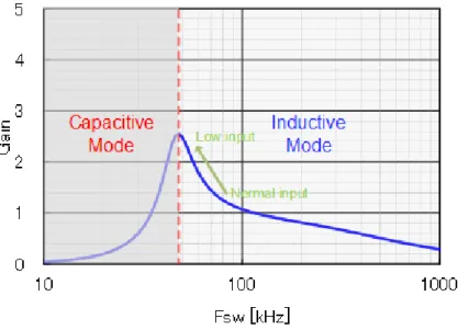
The first one is how to prevent capacitive mode [13]-[15] without the peak gain impact. Fig. 1-5 shows a typical gain characteristics of LLC resonant converters. The left region with boundary of peak gain is called capacitive mode region which may cause power MOSFETs fail. When the input voltage decreases, the switching frequency goes down to meet the requirement of gain. Before the gain reaches to the peak point, the switching frequency should not go down again to avoid capacitive mode. Considering the
tolerance of the resonant tank, it is not easy to determine the minimum operating voltage without the peak gain impact.
The second one is how to detect the load condition at the primary side accurately. Even though the LLC resonant converters can achieve higher power conversion efficiencies than other PWM topologies at nominal load condition [16], the efficiencies cannot be satisfied at light load conditions.
Fig. 1-6 shows the efficiency curve against output power at general DC-DC converters. The best performance in terms of efficiency takes place at the middle load conditions. In order to improve the efficiency at light load conditions, burst mode control
Fig. 1-7. Switching state at normal mode and burst mode.
techniques are used popularly as shown in Fig. 1-7. Here, the normal mode means that the switching states keep operating without stop. On the other hand, at burst mode, the switching state is between operation and stop periodically. For example, when the output power is Po_llat the normal mode, the relation of Po_lland Po_mlat the burst mode can be
expressed as (1-2) bst p on p ml o ll o
t
t
P
P
_ _ _ _
(1-2)Here tp_onis the switching operation period and tp_bstis burst period. At burst mode, since
the output power at the switching operation period belong to the middle power of the converter, the best efficiency can be obtained despite of the light load condition.
As for burst mode control techniques at light load conditions[17]-[18], if the load is lighter than a lower predetermined load level, the operation mode of the LLC converters is switched from normal mode to burst mode. On the other hand, if the load is heavier than an upper predetermined load level, it is switched from burst mode to normal mode [19]. In order to realize automatic burst mode control which is switching operation between normal mode and burst mode automatically, the control systems need to obtain load conditions accurately at both normal mode and burst mode. For off-line converters, detecting the load condition at the primary side is preferred to the secondary side in terms of cost performance. For example, feedback signals which control the pulse widths of power switches are used to reflect the load conditions in pulse width modulation (PWM) control topologies. However, it is difficult for the LLC resonant converters belonging pulse frequency modulation (PFM) control topologies to reflect the load conditions with the feedback signals which control the switching frequencies. This is because the switching frequencies are almost constant if it is set near the resonant frequency even though the load changes dramatically [20].
For LLC resonant converters with low power, shunt resistors are used to reflect the load conditions at the primary side as expressed in [21]. But shunt resistors cannot be recommended for LLC resonant converters with the nominal power of over 100W, because the power loss of the shunt resistors is proportional to the nominal power.
method is described as [19]. However, it is inaccurate not to consider some parasitic capacitances [23]-[24] according the analysis of [22]. A resonant current or voltage sensing method with a lossless network to detect the load conditions is shown in Fig. 1-8 according to [25]-[26]. But it is not suitable for normal mode and especially burst mode at light load conditions since the sensing network works like a divider for the ripple voltage on Cr as described in [25], which has insufficient load dependence.
Fig. 1-8. Circuit diagram of a LLC resonant converter with a conventional load detection circuit.
1.4 Objective and Outlines
In this dissertation, for off-line converters, the objective is to achieve high efficiency at light load condition by automatic burst mode control for LLC resonant topology, and high density by simplifying EMI filter, bulk capacitors and thermal management.
This dissertation consists of five chapters which are organized as below.
Chapter 1 describes the background of opportunities and challenges of the interested off-line converters including CCM boost PFC converters and LLC resonant converters. High efficiency, especially at light load conditions, and high power density are the trends for these applications.
For CCM boost PFC converters, in order to achieve high power density by simplifying the EMI filter, high switching frequency is necessary but not enough since there is a trade-off relation between high switching frequency and high efficiency.
Regarding LLC resonant converters, they are good at operating with a wide input voltage range. In terms of holdup time requirement [27]-[28], the wide input voltage range can provider high power density by reducing the bulk capacitors. However, the wide input voltage range has a risk of capacitive mode which may cause the power MOSFET fail.
What’s more, recently burst mode control is studied to obtain high efficiency at light load conditions for the LLC resonant dc-dc converters. But it is so difficult to detect load condition at the primary side of the dc-dc resonant converter to realize automatic burst mode control. The high cost impact due to the secondary load detection prevents burst mode control from spreading. At the same time, a precise overload protection is desired to improve the thermal design for high power density of the LLC resonant off-line converters.
Chapter 2 presents a novel spread spectrum method for CCM boost PFC converter operating in average current mode control to optimize both conducted EMI and efficiency. A new analysis method is proposed with the 3rd harmonic components of the boost
inductor current ripple by Fourier Transform. The proposed method induces a type frequency modulation with maximum and minimum frequency limits. By the saddle-type frequency modulation, the improved conducted EMI performance is obtained
without the sacrifice of efficiency, resulting in a simplified conducted EMI filter experimentally.
In Chapter 3, a novel anti-capacitive mode protection is provided to improve the trade-off between the wide input voltage range and anti-capacitive mode protection, beginning with a brief review of topologies of the LLC resonant converters. A reliable detection method of the capacitive mode is proposed by using the resonant current and resonant voltage. The input voltage range is optimized so that the bulk capacitor can be smaller to get higher power density.
In Chapter 4, burst mode control techniques have been studied for LLC resonant off-line converters to improve power conversion efficiencies at light load conditions. We propose and implement a lossless load detection technique for normal and burst mode by a novel average input current sensing method at the primary side of LLC resonant converters. Detailed theoretical analysis at normal and burst mode is presented and a load detection circuit is proposed with the consideration of integrated circuits. To verify the analysis, an LLC resonant off-line converter with 400V input and 16V/10A output is simulated using PSIM and a prototype board is built. The experimental results show that the proposed load detection technique is valid and practical. As a result, an automatic burst mode control for LLC resonant converters at light load conditions is realized with the proposed average input current sensing method. At the same time, a precise overload protection is realized to improve the thermal design, resulting a higher power density.
In the final chapter, conclusions is given and then the plans for future work is described.
References
[1] “The twin pillars of sustainable energy: synergies between energy efficiency and renewable energy technology and policy”. [Online] Available: citeseerx.ist.psu.edu. [2] “Efficiency Standards for External Power Supplies”, [Online] Available:
www.jp.cui.com.
[3] “Energy Conservation Program: Test Procedures for External Power Supplies”, [Online] Available: www.energy.go.
[4] “Harmonic current emissions guidelines to the standard EN 61000-3-2”, [Online] Available: www.epsma.org.
[5] “Internatioanl special committee on radio interference (CISPR)”, [Online] Available: www.iec.ch.
[6] W. P. Zhang,W. Zhang,J. Yang,F. Al-Naemi, “Comparisons between CRM and CCM PFC”, Energy and Power Engineering, May, 2013, pp. 864-868.
[7] “SiC schottky diodes in power factor correction” [Online] Available: www.wolfspeed.com.
[8] B. Lu, W. Dong, S. Wang, F. C. Lee, “High Frequency Investigation of Single-switch CCM Power Factor Correction Converter”, in Proc. 19th Annu. IEEE Appl. Power
Electro. Conf. and Expo., Feb., 2004, pp. 1481–1487.
[9] “PFC Pre-Regulator Frequency Dithering Circuit”, SLUA424A, [Online] Available: www.ti.com.
[10] H. Wang, S. Dusmez, A. Khaligh, “A Novel Approach to Design EV Battery Chargers Using SEPIC PFC Stage and Optimal Operating Point Tracking Technique for LLC Converter”, in Proc. 29thAnnu. IEEE Appl. Power Electro. Conf. and Expo.,
Feb., 2014, pp. 1683–1489.
[11] L. Zhang, H. Wang, “Comparative Analysis of High Step-down Ratio Isolated DC/DC Topologies in PEV Applications”, in Proc. 31st Annu. IEEE Appl. Power
[12] H. Wang, “A Pulse Width Modulated LLC Type Resonant Topology Adpated to Wide Output Voltage Range”, in Proc. 31stAnnu. IEEE Appl. Power Electro. Conf.
and Expo., Feb., 2016, pp. 1280–1285.
[13] “LLC resonant half-bridge converter design guideline”, AN2450, [Online] Available: www.st.com.
[14] “Design of Resonant Half-Bridge converter using IRS2795(1,2) Control IC”, AN-1160, [Online] Available: www.infineon.com.
[15] “Understanding the LLC Structure in Resonant Applications”, AND8311/D, [Online] Available: www.onsemi.com.
[16] B. Yang, F. Lee, A. Zhang, G. Hua, “LLC resonant converter for front end DC/DC conversion,” in Proc. 17th Annu. IEEE Appl. Power Electron. Conf. Expo., 2002, pp. 1108-1112.
[17] W. Feng, F. Lee and P. Mattavelli, “Optimal Trajectory Control of Burst Mode for
LLC Resonant Converter,” IEEE Trans. Power Electron., vol. 28, no. 1, pp. 457-466,
Jan. 2013.
[18] S. Zhao, J. Xu, and O. Trescases, “Burst-Mode Resonant LLC Converter for an LED Luminaire With Integrated Visible Light Communication for Smart Buildings,” IEEE
Trans. Power Electron., vol. 29, no. 8, pp. 4392-4402, Aug. 2014.
[19] B. Wang, X. Xin, S. Wu, H. Wu, J. Ying, “Analysis and Implementation of LLC Burst Mode for Light Load Efficiency Improvement,” in Proc. 24th Annu. IEEE Appl.
Power Electron. Conf. Expo., 2009, pp. 58-64.
[20] H. Choi, “Analysis and Design of LLC Resonant Converter with Integrated Transformer,” in Proc. 22nd Annu. IEEE Appl. Power Electron. Conf. Expo., 2007, pp. 1630-1635.
[21] Y. Fang, D. Xu, Y. Zhang, F. Gao, L. Zhu, Y. Chen, “Standby Mode Control Circuit Design of LLC Resonant Converter,” in Proc. IEEE Power Electron. Spec. Conf., Jun., 2007, pp. 726-730.
[22] Z. Hu, Y. Liu, P. Sen, “Cycle-by-cycle average input current sensing method for LLC resonant topologies,” in Proc. IEEE Energy Conv. Congr. Expo., 2013, pp. 167-174.
[23] B. Lee, M. Kim, C. Kim, K. Park and G. Moon, “Analysis of LLC Resonant Converter Considering Effects of Parasitic Components,” in Proc. IEEE Telecommun.
Energy Conf., 2009, pp. 1-6.
[24]“ Half bridge resonant LLC converters and primary side MOSFET selection”, AN4720, [Online] Available: www.st.com.
[25] “Application Note for an LLC Resonant Converter Using Resonant Controller HR1000”, AN054, [Online] Available: www.MonolithicPower.com.
[26] “L6598 off-line controller for Resonant Converters”, AN1673, [Online] Available: www.st.com.
[27] B. Lu, W. Liu, Y. Liang, and F. Lee, “Optimal Design Methodology for LLC Resonant Converter” in Proc. 21st Annu. IEEE Appl. Power Electron. Conf. Expo.,
2006, pp. 533-588.
[28] S. Hong, S. Cho, C. Roh, and S. Han, “Precise Analytical Solution for the Peak Gain of LLC Resonant Converters”, Journal of Power Eletronics, vol. 10, no. 6, pp. 680-685, Nov., 2010.
Chapter 2
Spread spectrum method for CCM boost PFC converters
2.1 Introduction of boost PFC converters
Boost PFC converters are used to correct the power factor (PF) and regulate the line AC voltage to a stable DC voltage at an AC electrical power system. Fig. 2-1 shows a typical schematic diagram of a boost PFC converters with the input line voltage from 90Vac to 264Vac.
As a boost converter, the DC output voltage is set more than the DC voltage of 372V, which is the peak value of 264Vac, and is set as 390V to 400V generally. As a PFC converters, the PF is regulated near 1. In other words, the PFC converter looks like a resistor in terms of AC power supply no matter how the line voltage or load changes as shown in Fig. 2-2.
Fig. 2-2. The equivalent diagram of the boost PFC converter. Fig. 2-1. Typical schematic diagram of the boost PFC converter.
PF is defined as the ratio of the real power PRto the apparent power PA as expressed in (2-1). d I d V d I V P P PF AC AC AC AC A R
0 2 0 2 0 (2-1)Here θ is a variable indicating a phase angel in the range of 0 to π or 0° to 180° in terms of degree.
In order to obtain PF near 1, IACis controlled to have the same phase with VACas much
as possible by means of the boost PFC converters. According to the current iLof the boost
(a)
(b)
(c)
inductor, the operation modes can be specified as: continuous conduction mode (CCM), critical conduction mode (CRM) and discontinuous conduction mode (DCM) as shown in Fig. 2-3.
Because CCM PFC operates in average current mode with fixed switching frequency, it is easy to design the boost inductor and the EMI filter thanks to the relatively small ripple current of the boost inductor. Therefore, CCM is a good choice in terms of power density [1], especially the existence of SiC diode [2].
2.2 Analysis of 3
rdharmonic component of inductor current
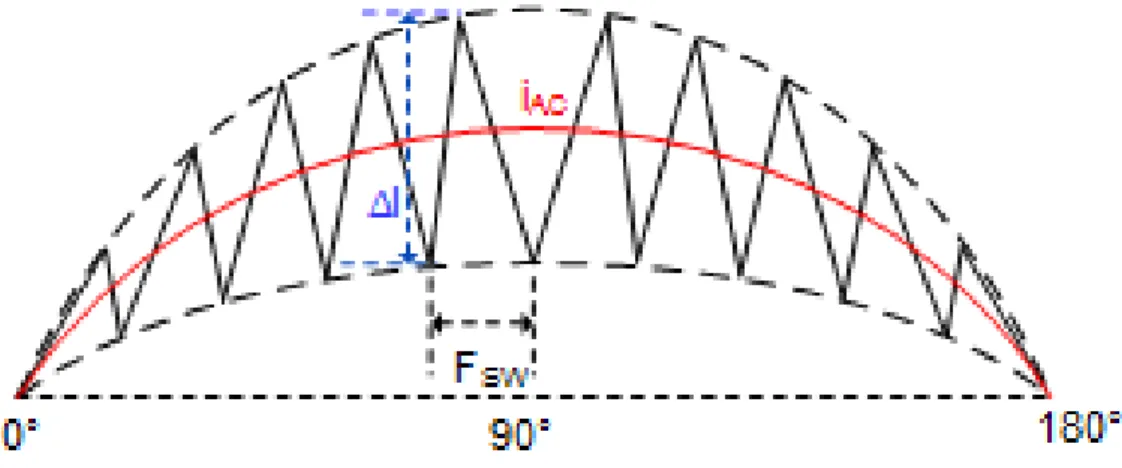
For CCM boost PFC converters, the current ripple waveform of the boost inductor iL
is triangular as shown in Fig. 2-4.
The current ripple of the boost inductor can be expressed as (2-2)
SW ac F L D V I () 2 sin (2-2)
Here, Vac and θ is the effective value and the phase of the input line voltage respectively, L is the inductance of the boost inductor, Fswis the switching frequency and D is the duty
of the switching cycle which is defined as (2-3).
O ac
V V
D1 2 sin (2-3)
Here, VOis the output voltage of the boost PFC converter.
Therefore, the current ripple of the boost inductor can be expressed as (2-4). ) sin 2 1 ( sin 2 ) ( O ac SW ac V V F L V I (2-4)
It is clear that the current ripple can be seen as a triangular waveform since the switching frequency is much higher than the frequency of the input line voltage.
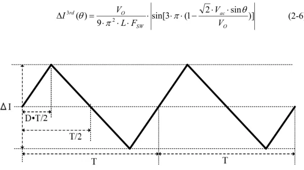
For Triangle waveform as shown in Fig. 2-5 [3], the Fourier series is
) sin( ) 1 ( ) sin( _ ) ( 1 2 2 t n D D n D n I n t i
(2-5)When we do the Fourier analysis for the current ripple of the boost inductor, the amplitude of the harmonic component can be achieved by (2-5).
According to the CISPR-22 standard, sine the limit of quasi-peak (QP) level starts from 150kHz, at the applications with the switching frequency between 50kHz and 70kHz, it is not necessary to take into account the 1stand 2ndharmonic component except the 3rd
one. Therefore, the amplitude of the 3rdharmonic component of the current ripple can be
deduced as (2-6). )] sin 2 1 ( 3 sin[ 9 ) ( 2 3 O ac SW O rd V V F L V I (2-6)
From (2-6), we can see that the value of the 3rd harmonic component is inversely
proportional to the switching frequency and depends upon the input line voltage. On the other hand, the maximum value of the 3rd harmonic component is independent on the
input line voltage.
The normalization of the 3rdharmonic component can be expressed as (2-7).
)] sin 2 1 ( 3 sin[ ) ( 3 rd V nor k I (2-7) Here O ac V V V k .
Similarly, according to (2-4), the normalization of the current ripple can be expressed as (2-8).
Inor() kV sin(1 2kV sin) (2-8)
The normalization of the current ripple and the 3rdharmonic component, where k
Vis
0.20, 0.25 and 0.30 which represent the typical value of the low line voltages, is shown
Fig. 2-6. The normalization of the current ripple 0.00 0.05 0.10 0.15 0.20 0 45 90 135 180 N or m al iz at io n of th e cu rr en t r ip pl e of t he b oo st in du ct or
The phase of the input line voltage [º] k=0.20
k=0.25 k=0.30
as Fig. 2-6 and Fig. 2-7 respectively. In Fig. 2-6, since the peak current appears in the vicinity of 90 degree of the input line voltage, the maximum value of the switching loss appears in the vicinity of 90 degree too.
On the other hand, as shown in Fig. 2-7, it can be seen that the worst-case value of the 3rdharmonic component takes place in the vicinity of 30 degree or 150 degree instead of
that of 90 degree.
Consequently, when kVis 0.20~0.30, we should improve the power loss in the vicinity
of 90 degree with minimum switching frequency because the switching loss is proportional to the switching frequency, and reduce the 3rdharmonic component in the
vicinity of 30 degree and 150 degree with maximum switching frequency because the higher the switching frequency, the more worst-case quasi-peak margin we can obtain based on the explanation of the chapter 1. As a result, we can achieve the optical design between the efficiency and the EMI filter.
Fig. 2-7. The normalization of the 3rdharmonic component 0.0 0.2 0.4 0.6 0.8 1.0 0 45 90 135 180 N or m al iz at io n of th e 3r d ha rm on ic c om po ne nt
The phase of the input line voltage [º] k=0.20
k=0.25 k=0.30
2.3 Analysis of spread spectrum method for simplifying the EMI filter
In a universal off-line converter application with output voltage of 390V and load of 600W, Fig. 2.8 shows an experimental CCM boost PFC converter with a conducted EMI filter. In order to reduce the switching power loss, the switching frequency is subject to 55kHz.
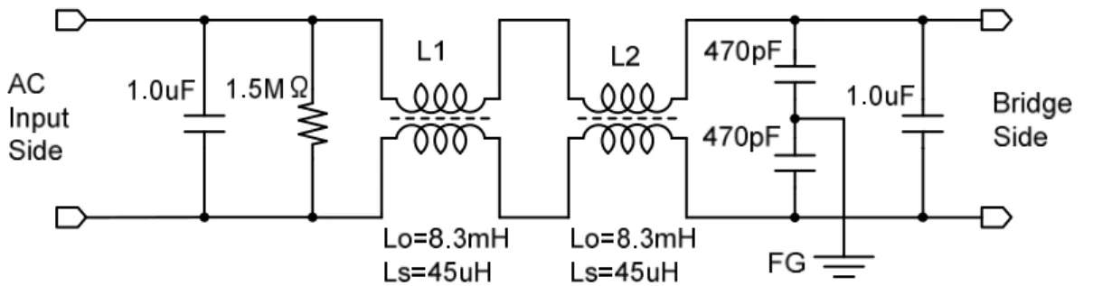
In order to obtain enough worst-case quasi-peak margin, the conducted EMI filter is designed with two choke coils as shown in Fig. 2-9 and Fig. 2-10. It should be noted that Fig. 2-10 is an example but not exact the EMI filter used in this work. The objective of this chapter is to remove one choke coil with the same worst-case quasi-peak margin performance.
Fig. 2-8. Simplified schematic diagram of a 600W boost PFC converter
Based on the analysis of 3rd harmonic component of the inductor current ripple, a
novel spread spectrum method is presented to simplify the EMI filter without the sacrifice of the efficiency.
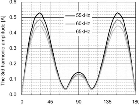
In the case of 100Vac line voltage (kV= 0.256) and 600W output power , the amplitude
of the 3rd harmonic component is shown in Fig. 2-11 which illustrates the worst-case
value takes place in the vicinity of 30ºand 150ºinstead of 90º. Therefore, it’s enough just
Fig. 2-11. The 3rdharmonic component of the inductor current ripple at 100Vac 0.0 0.1 0.2 0.3 0.4 0.5 0.6 0 45 90 135 180
The phase of the input line voltage [º]
T he 3 rd h ar m on ic a m pl itu de [ A ] 55kHz 60kHz 65kHz
to increase the switching frequency in the vicinity of 30 and 150 degree to reduce the 3rd
harmonic amplitude.
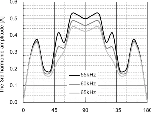
In the case of 240Vac (kV= 0.615) and 600W, the 3rdharmonic amplitude is shown in
Fig. 2-12 where the worst case appears at the phase of around 90 degree. So, it is important to increase the switching frequency in the vicinity of 90 degree in order to reduce the 3rd
harmonic amplitude. It is worth noting that Fig. 2-12 is calculated by taking into account the discontinuous boost current which appears in the case of high input line voltage due to low inductance value of the boost inductor.
Fig. 2-12. The 3rdharmonic component of the inductor current ripple at 240Vac
0.0 0.1 0.2 0.3 0.4 0.5 0.6 0 45 90 135 180
The phase of the input line voltage [º]
T h e 3 rd h a rm o n ic a m p lit u d e [ A ] 55kHz 60kHz 65kHz
2.4 Spread spectrum design of control IC
According to the above analysis, it is proposed to modulate the switching frequency as a function of the input line voltage (VAC) and the input line current (iAC) with maximum
(FSW_MAX) and minimum (FSW_MIN) frequency limits. Since the input line current is
inversely proportional to the input line voltage when the load is same, it can be used to come up with the dependence between the 3rd harmonic component and the input line
voltage.
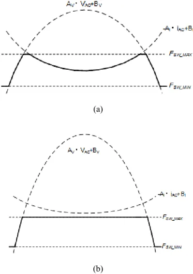
The image of the modulated switching frequency is shown in Fig. 2-13.
(a)
(b)
Fig. 2-13. The image of the modulated switching frequency (a) Low input line voltage (b) High input line voltage
-31-The modulated switching frequency (FSW) is given by
SW MAX V AC V i AC i SW MIN
SW MAX MIN F MIN A V B A i B F
F ( _ , ( , )), _ (2-9)
Where AV, BV, Aiand Biare positive constants.
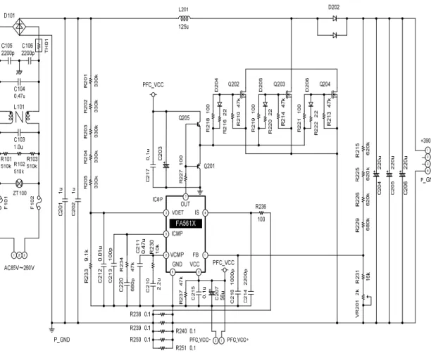
Based on (2-9), the spread spectrum control method for PFC converters is realized by CCM PFC controller IC FA5610 series which were released by Fuji Electric Corporation. The demo board is shown as Fig. 2-14 [4], where there is only one choke coil used in the EMI filter.
-32-2.5 Experimental results
The modulated switching frequency is shown in Fig. 2-15 and Fig. 2-16 at the input line voltage of 100Vac and 240Vac respectively. In the case of 100Vac, a saddle-type switching frequency is obtained to keep the efficiency performance due to the switching frequency of 60kHz at 90ºand to reduce the generation of the conducted EMI due to that of 68kHz at 30º
and 150º. The switching frequency is controlled by the input line current at the phase period
of 30 degree to 150 degree and the other phase period is controlled by the input line voltage, as explained in Fig. 2-13 (a).
Fig. 2-15. Modulated switching frequency at 600W output at 100Vac 45 50 55 60 65 70 75 0 45 90 135 180
The phase of the input line voltage[º]
T he s w itc hi ng f re qu en cy [ kH z]
-33-In the case of 240Vac, it mainly works on the maximum frequency limits to reduce the EMI without efficiency issue owing to the lower current of the boost inductor. The switching frequency is controlled by the maximum frequency limits at the phase period of 15 degree to 170 degree and the other phase period is controlled by the input line voltage, as explained in Fig. 2-13 (b).
Fig. 2-16. Modulated switching frequency at 600W output at 240Vac
45 50 55 60 65 70 75 0 45 90 135 180
The phase of the input line voltage[º]
T he s w itc hi ng f re qu en cy [ kH z]
-34-Fig. 2-17 and -34-Fig. 2-18 show the EMI noise magnitude with comparison between conventional fixed 55kHz with two choke coils and proposed modulated switching frequency with one choke coil at 100Vac and 240Vac respectively. It is clear that the worst-case margin of QP level with one choke coil is same as that of QP level with two choke coil thanks to the proposed spread spectrum method.
Fig. 2-17. Noise magnitude comparison at 100Vac
20 30 40 50 60 70 80 0.1 1 N oi se M a gn itu d e [d B u V ] Frequency [MHz]
Modulation with one choke coil Fixed 55kHz with two choke coils
QP Ave
Fig. 2-18. Noise magnitude comparison at 240Vac
20 30 40 50 60 70 80 0.1 1 N o is e M a g n itu d e [ d B u V ] Frequency [MHz]
Modulation with one choke coil Fixed 55kHz with two choke coils
QP Ave
-35-Fig. 2-19 shows the efficiency from light load to nominal load at the input voltage of 100Vac. It can be seen that the efficiency at the operation mode of modulation with one choke coil is higher than that at the operation mode of fixed 55kHz with two choke coils from light load to nominal load.
In terms of the worst-case quasi-peak margin and the efficiency recorded in Table 2-1, it is clear that one choke coil in Fig. 2-6 can be removed by the comparison between fixed 55kHz switching frequency with two choke coils and modulated switching frequency with one choke coil.
Fig. 2-19. Efficiency comparison at 100Vac 93.5 94.0 94.5 95.0 95.5 96.0 96.5 50 100 150 200 250 300 350 400 450 500 550 600 E ffi ci en cy [ % ] Output power [W] Modulation with one choke coil Fixed 55kHz with two choke coils
Table 2-1
Comparison of the worst-case quasi-peak margin and the efficiency
Switching Frequency Fixed 55kHz Modulation
The number of choke coils 2 1
The worst-case quasi-peak margin 100Vac 14.7dB 14.3dB 240Vac 15.3dB 15.0dB Efficiency 100Vac 93.7% 93.8% 240Vac 97.9% 97.8%
-36-2.6 Conclusion
At CCM boost PFC converters, there is a trade-off relation between small EMI filters and high efficiency with conventional spread spectrum method . A novel spread spectrum method is presented to optimize both conducted EMI and efficiency. A new analysis method is proposed with the 3rd harmonic components of the boost inductor current ripple by Fourier
Transform. The proposed method induces a saddle-type frequency modulation with maximum and minimum frequency limits. By the saddle-type frequency modulation, the improved conducted EMI performance is obtained without the sacrifice of the efficiency, resulting in a simplified conducted EMI filter experimentally.
-37-References
[1] W. P. Zhang,W. Zhang,J. Yang,F. Al-Naemi, “Comparisons between CRM and CCM PFC”, Energy and Power Engineering, May, 2013, pp. 864-868.
[2] “SiC schottky diodes in power factor correction” [Online] Available: www.wolfspeed.com.
[3] J. Bleslin, W. Hurley, “Derivation of Optimum Winding Thickness for Duty Cycle Modulated Current Waveshapes” in Proc. 28thAnnu. IEEE Power Electron. Spec. Conf.,
1997, pp. 655-661.
[4] “低ノイズ電流連続モード PFC 制御 IC「FA5610/FA5611」[Online] Available: www.fujielectric.com
-38-Chapter 3
Control method for anti-capacitive mode of LLC resonant
converters
3.1 Introduction of LLC resonant topologies
In previous chapter, the PFC parts of off-line power supplies have been discussed. In this chapter and the next one, the isolated LLC resonant converter of the off-line power supplies will be presented.
This chapter presents control methods of anti-capacitive mode, beginning with a brief review of topologies of LLC converter. Regarding load condition detection method, it will be presented in chapter 4.
For resonant converter topologies, their output voltage is regulated by changing the frequency of the driving voltage such that the impedance of resonant tank LC changes, as shown in Fig. 3-1. The output voltage can be expressed as
R sw LC R i o Z f Z Z V V ) ( (3-1)
-39-Here, ZRis the impedance of load, ZLC(fsw) is the impedance of resonant tank LC.
When the load changes from nominal conditions to light load conditions, the impedance variations of the load is so large that it is difficult to regulate the output voltage. It is because the frequency can’t be controlled infinitely to get enough impedance variations of ZLC(fsw).
To solve this problem, a quasi-load ZL is added as shown in Fig. 3-2. Even though no
load conditions happens, the quasi-load will limit the variation of the frequency fsw. At this
time, the output voltage is
) /( ) ( ) /( L R L R sw LC L R L R i o Z Z Z Z f Z Z Z Z Z V V (3-2)
Here, ZLrefers to reactive impedance.
When ZL is provided by an inductor or a magnetic part of a transformer, this kind of
converter is named as LLC resonant converter.
-40-Fig. 3-3 shows a LLC resonant converter of the isolated off-line dc-dc power supply, based on Fig. 3-2.
In Fig. 3-3, there are three parts including the switch circuit, the resonant circuit and the load circuit. At the switch circuits, Vishown in Fig. 3-2 is generated with four switches, so
called full bridge topology.
At the resonant circuit, ZLC(fsw) is consisted with the resonant inductance of Lr , the
resonant capacitance of Cr, and the magnetizing inductance of Lm. ZLshown in Fig. 3-2 is
provided by the magnetizing inductance of Lm which is generally four to six times larger than that of Lr.
At the load circuit, load is isolated with the primary side by transformer T1, and the output voltage is rectified by four diodes and capacitor Co, which we call them full wave rectifier. It is noted that at the application with high output voltage of more than about 60V, the full wave rectifier is popular.
-41-As showed in Fig. 3-4, for middle power applications with power range of about 100W~500W, half bridge topology is commonly used. Here, the resonant capacitance is the sum of Cr_H and Cr_L. For low output voltage applications with output range of about 5V~60V, half wave rectifier is a better choice.
Generally, Lr, Lm and T1 are integrated into one transformer as shown in Fig. 3-5 [1].
Fig. 3-4. LLC resonant converter with half bridge topology
-42-In applications of off-line power supplies, half bridge topologies with one resonant capacitor are common as shown Fig.3-6 and Fig.3-7.
Fig. 3-6. LLC resonant converter with high side resonant capacitor
-43-3.2 Anti-capacitive mode technique
In this section, a control method of anti-capacitive mode is presented. In terms of the minimum effective input voltage where the nominal load can be remained, it is optimized automatically by detecting the resonant current and resonant voltage. As a result, the capacitance of the bulk capacitor can be as less as one thirds compared with that in the conventional control method. It is noted that, in this paper, the topology shown in Fig. 3-7 is used and simulation waveforms are implemented using PSIM with parameters listed in Table 3-1.
Based on the first harmonic approximation [2]-[4], the gain curve against switching frequency is shown as Fig. 3-8, where the nominal load is set as 160W.
Fig. 3-8. Gain curve against switching frequency
0 1 2 3 4 5 10 100 1000 G ai n Fsw [kHz] 160 W 100 W 50 W
-44-When the input voltage decreases, the switching frequency goes down to meet the requirement of the gain, as shown in (3-3).
in o G V V N K 2 (3-3)
Where KGis the gain which is necessary to keep the output voltage Vo, N is turns ratio of the
primary side to the secondary side.
Before the gain reaches to the peak point, the switching frequency should not go down again to avoid capacitive mode as discussed in section 1.3.
Table 3-1
Parameters for simulation
Symbol Designed parameters Parameter value
Vin Input voltage 400V
Vo Output voltage 16V
LO Inductance of primary winding
with secondary winding open 568μH LS Inductance of primary windingwith secondary winding short 150μH
N Turns ratio 48:3:3
CR Capacitance of Resonant capacitor 22nF
Ron On resistance of Qa or Qb 0.49Ω
VF Forward voltage of Da or Db 0.5V
Cs Capacitance of current divider 220pF
-45-Fig. 3-9 shows the waveform of the input current Iin, the resonant current ICr, the resonant
voltage VPr which is impressed at the primary side of the integrated transformer, and the
output current Io. When the input voltage Vin goes down to 150V, the capacitive mode
happens due to the recovery characteristic of the body diodes of the power MOSFETs. It can be seen that there is surge current at the input current waveform. Such condition may cause the MOSFET power switches fail due to the dI/dt issue. It is noted that the value of the surge current shown in Fig. 3-9 is more than 20A when performing experimental measurement.
-46-When the input voltage goes down from normal input voltage of 400V, it can be seen clearly that the resonant tank includes two resonant regions, LC region with LSand CR, and
LLC region with LOand CR, as shown in Fig. 3-10.
The resonant frequency fLCof LC region is
R S LC C L f 2 1 (3-4) The resonant frequency fLLCof LLC region is
R O LLC C L f 2 1 (3-5)
-47-In order to avoid capacitive mode automatically which is called anti-capacitive mode generally, as shown in Fig. 3-11, the proposed method have two steps as below.
Step1: Detecting LLC region by monitoring the resonant voltage VPr.
Step2: Turn off the MOSFET power switches by monitoring the resonant current ICr.
For example, when the high side switch is on, the resonant voltage VPr is monitored
whether VPrbecomes lower than a predetermined voltage VPr_th. If VPr < VPr_th, the resonant
tank enters the LLC region and go to step2. The resonant current ICris detected whether ICr
becomes lower than a predetermined current ICr_th. If it is, then turn off the high side switch.
Fig. 3-11. The proposed control method by detecting resonant voltage and resonant current
-48-Fig. 3-12 shows the waveforms where Vingoes down from 400V to 150V according to the
proposed control method with anti-capacitive mode. It can be seen that no capacitive mode happens even though Vinis set as 150V.
Input voltage of 300V Input voltage of 400V
Input voltage of 200V Input voltage of 150V
-49-3.3 Optimization of the bulk capacitor
Due to the proposed control method, the minimum effective input voltage can be optimized automatically to simplify the bulk capacitor.
In terms of holdup time, the capacitance can be expressed as (3-6).
) ( 2 2 _ 2 _nom in min in hold o bulk V V T P C (3-6)
Where Pois nominal power, Tholdis holdup time, ηis conversion efficiency, Vin_nomis nominal
input voltage and Vin_minis the minimum effective input voltage. Fig. 3-13 show the relation
between Cbulk and Vin_minaccording to (3-6), here, Po = 160W, Thold= 20ms, η = 0.95, and
Vin_nom= 400V.
It can be seen that if the Vin_minis set as 360V, a bulk capacitor which has capacitance of
220μF is need. However, when Vin_min can go down to 200V, the capacitance of 68μF is
enough. As a results, the capacitance of the bulk capacitor can be as less as one thirds compared with the conventional control method.
Fig. 3-13. Capacitance of bulk capacitor against the minimum effective input voltage
0 50 100 150 200 250 300 200 250 300 350 400 C ap ac it an ce o f B ul k C ap ac it or [ uF ] Vin_min [V]
-50-3.4 Conclusion
At the LLC resonant off-line converter, one of the challenges is how to prevent capacitive mode without the peak gain impact, resulting small bulk capacitors and robust LLC resonant converters. A novel anti-capacitive mode technique is provided to improve the trade-off between the wide input voltage range and anti-capacitive mode. A reliable detection method to avoid the capacitive mode is proposed by detecting the resonant current and resonant voltage. The input voltage range is optimized so that the bulk capacitor can be smaller to get higher power density for the LLC resonant off-line converters
-51-References
[1] H. Choi, “Analysis and Design of LLC Resonant Converter with Integrated Transformer,” in Proc. 22nd Annu. IEEE Appl. Power Electron. Conf. Expo., 2007, pp. 1630-1635. [2] R. Steigerwald, “A comparison of half-bridge resonant converter topologies,” IEEE
Trans. Power Electron., vol. 3, no. 2, pp. 174-182, Apr. 1988.
[3] T. Duerbaum, “First harmonic approximation including design constraints,” in Proc. IEEE Telecommun. Energy Conf., 1998, pp. 321-328.
[4] H. Huang, “FHA-Based Voltage Gain Function with Harmonic Compensation for LLC Resonant Converter,” in Proc. 25th Annu. IEEE Appl. Power Electron. Conf. Expo., 2010, pp. 1770-1777.
-52-Chapter 4
Load detection techniques of LLC resonant converters
4.1 Improved LLC resonant converters
In this section, a lossless load detection technique is presented for improving the efficiency at light load condition by realizing an automatic burst control, and for improving the thermal design by realizing a precise overload protection.
A LLC resonant DC-DC converter including a proposed load detection circuit with the isolation between the primary side and the secondary side is shown in Fig. 4-1.
In the main power circuit, there are a high-side part and a low-side part at the primary side. At the high-side part, there are a power MOSFET Qa with a body-diode BDa, and a capacitor Ca with the output capacitance of Qa and extra capacitance if have. In the low-side part, there are Qb, BDb and Cb same as the high-side part, and a resonant tank including resonant
Fig. 4-1. Circuit diagram of a LLC resonant converter with a proposed load detection circuit by resonant current sensing.
Da Db n:1:1 Cr Lr Lm Vin Qa Qb Driving Circuit Vo Ro Ci T1 Cs Rs HO LO IS VS FB Load detection
Control circuit VCO
Rfb VDD SR1 R1 R2 R3 R4 C2 PC1 Primary Secondary Ca Co Iin Isolation BDa BDb Cb CA Proposed load detection circuit
-53-inductor Lr, magnetizing -53-inductor Lm and resonant capacitor Cr. There is an ideal transformer T1 with center-tapped structure by which energy is transferred from the primary side to the secondary side with isolation. Generally, Lr, Lm and T1 are integrated into one transformer as described in chapter 3. At the secondary side, there are two rectifier diodes Da and Db, a rectifier capacitor Co and the output resistor Ro called as load.
In the control circuits of the primary side, the control units are integrated into one control IC, except some big capacitors etc. There are a driving circuit, a control circuit unit, a voltage-controlled oscillator VCO, and the proposed load detection circuit with two input signals and one output signal. One input signal of the load detection circuit is a voltage level VISwhich
reflect the resonant current (ILr) through a current divider Cs and Rs, which is called “lossless”
sensing technique with capacitive shunt [1]. The other one is a voltage level VVSwhich is the
drain voltage of the low-side power MOSFET Qb. It is noted that the VVSis approximately
detected by an auxiliary winding at the primary side of the transformer when implementing the experiment to simplify the control IC. The output signal of the load detection circuit is a voltage level VCA which reflects the load conditions. The unit of control circuit determines
the operation mode such as normal and burst mode at light load conditions according to VCA
by comparing with predetermined levels.
The isolation of the control circuit between the primary side and the secondary side is implemented by a photo-coupler PC1, a shunt regulator SR1 and phase compensation parts R1, C2 and R2 etc.
-54-4.2 Analysis and design of load detection technique
In this section, detailed theoretical analysis for load detection technique at both normal mode and burst mode is presented and a load detection circuit is proposed with the consideration of integrated circuits. And then, a statistical analysis for overload detection is performed.
A. Normal Mode Operation
A typical operation waveforms (discontinuous conduction mode) of the LLC resonant converters at normal mode is shown in Fig. 4-2 [2]-[3]. Generally, the output power can be expressed as (4-1) for periodic switching operation.
dt t I T V P P T in p in in o p ) ( 1 0
(4-1) Here, Pinis the input power of the LLC resonant converter, Pois the output power, η is thepower conversion efficiency, Vin is the input DC voltage with a constant value, Tp is the
switching period of the resonant operation, Iin(t) is the input current which is a function of
time.
Fig. 4-2. Typical waveforms of LLC resonant converters
VVS s1 Iin ILr t0 t1 t2 t3 t4 s2 s3 s4 Tp VHO VLO
-55-The input current Iin(t) can be separated into four operation states as shown in Fig. 4-2.
According to (1), the output power can be expressed as (4-2).
) ) ( ) ( ) ( ) ( ( 1 4 4 3 3 3 2 2 2 1 1 1 0 dt t I dt t I dt t I dt t I T V P t is t is t t is t t is t t p in o
(4-2)Where, Iis1(t), Iis2(t), Iis3(t) and Iis4(t) stand for the input current at the states of s1,s2,s3and s4,
respectively.
The states of s1and s3are the transition states with the discharge or charge of Ca, Cb and
other parasitic capacitances by the current flowing through Lr as shown in Fig. 4-3 and Fig. 4-4. In this paper, the parasitic capacitances [11]-[12] are ignored since they have no effect on the analysis of the proposed load detection technique.
At the transition state s1, Ca is discharged by the part of the resonant current ILr, which is
equal to the input current Iin, and the voltage of Ca (VCa) is discharged from Vinto 0V. At the
transition state s3, Ca is charged by the part of resonant current ILr, which is equal to the input
current Iintoo, and VCais changed from 0V to Vin. Accordingly, the integration of the input
current at the state s1and s3of (4-2) can be given by (4-3) and (4-4), respectively.
Ca V dt t Iis in t t
( ) 1 1 0 (4-3) Ca V dt t Iis in t t
( ) 3 3 2 (4-4)
-56-Fig. 4-3. The transition state s1with discharge of Ca
-57-As for the state s2, it can be separated to five detailed states from state s2_1to state s2_5as
shown in Fig. 4-5. Here ILmis the magnetizing current flowing through Lm, IP_Ldis the load
current flowing through the primary side of the isolated transformer with ideal model.
Fig. 4-5. Typical waveforms of LLC resonant converters with detailed state s2.
ILr Iin IP_Ld ILm VVS VLO VHO t0 t1 s1 s2_1s2_2 0A 0A 0V 0V 0V 0A 0A s2_3 s2_4 s2_5 s3 s4 t2 t3 t4 Tp
-58-At the state s2_1, the power MOSFET Qa is still OFF and the resonant current flows
through the body-diode of Qa as shown in Fig. 4-6.
At the state s2_2, the power MOSFET Qa turns ON and the resonant current ILr flows
through the channel of Qa as shown in Fig. 4-7. It is clear that the resonant current is a part of the magnetizing current ILm.
Fig. 4-6. The state s2_1with the resonant current flowing through the body-diode of Qa.
-59-At the state s2_3, the resonant current is supplied by the bulk capacitor. The load current
IP_Ldcomes from the resonant current and the magnetizing one as shown Fig. 4-8.
At the state s2_4, the magnetizing current inverses and is supplied by the resonant current
as shown in Fig. 4-9.
Fig. 4-8. The state s2_3with the resonant current supplied by the bulk capacitor.
Fig. 4-9. The state s2_4with the resonant current supplying the magnetizing current and the
-60-At the state s2_5, the resonant current is same as the magnetizing resonant without the load
current flowing, as shown in Fig. 4-10.
During the state s2with s2_1to s2_5, it is clear that the input current Iinis always equal to
the resonant current ILr. Therefore the integration of the input current at the state s2of (4-2)
can be expressed as (4-5).
dt
t
I
dt
t
I
t Lr t is t t(
)
(
)
2 1 2 2 1
(4-5) As for the state s4, since Iis4(t) is zero, the integration of input current at the state of s4ofequation (2) can be expressed simply as (4-6).
0
)
(
4 4 3
I
ist
dt
t t (4-6)By substituting equation (4-3), (4-4), (4-5) and (4-6) into (4-2), the output power can be obtained as (4-7). dt t I T V P t Lr t p in o ( ) 1 2 1
(4-7) Fig. 4-10. The state s2_5with the resonant current same as the magnetizing current.
-61-It can be seen that the output power is directly proportional to the mean value of the resonant current during the state s2with period Tp. Since t1is the end timing of VS rising and
t2is the start timing of VS falling as shown in Fig. 4-2, the output power can be obtained by
detecting the resonant current ILr(t) and the timing of VS voltage VVS.
The resonant current ILr(t) can be detected by a current divider Cs and then transferred
into a voltage level VIS(t) with a resistor Rs as shown in Fig. 2. With the first harmonic
approximation [4]-[5] of the resonant current ILr(t), VIS(t)can be expressed as (4-8).
2 2 2 ) 2 ( ) 1 ( 2 ) 1 ( ) ( ) ( Cr Rs f Cs Cr Cr Rs f j Cs Cr R t I t V s s s Lr IS (4-8)
Where, fsis the frequency of the resonant current ILr(t).
And the phase shift (θVIS) of VIS(t) against ILr(t) can be expressed as (4-9).
Cr
Cs
Cs
Cr
Rs
f
s VIS
)
2
tan(
(4-9) Table 4-1Practical parameters for the current divider circuit.
Symbol Designed parameters Parameter value
Rs Resistance of current divider 220Ω
Cs Capacitance of current divider 220pF Cr Capacitance of resonant capacitor 22nF
-62-According to the practical parameters listed in the Table I, the parts with fs at (4-8) are
much smaller than other parts without fs, and can be ignored approximately. Therefore VIS(t)
can be expressed simply as (4-10)
)
(
)
(
)
(
Cr
Cs
Cs
Rs
t
I
t
V
IS Lr
(4-10)It is noted that even the operating frequency is up to 500kHz, the tolerance of (4-10) compared with (4-8) is only 1.1%. It is because the fs parts appear at both numerator and
denominator in (4-8).
According to (4-9), the propagation delay Tdly from ILr(t) to VIS(t) as shown in Fig. 4-11
can be expressed approximately as (4-11)
)
(
Cs
Cr
Cr
Cs
Rs
T
dly
(4-11)Here, tan(VIS ) VIS and VIS 2 fs Tdly are used.
Fig. 4-11. Waveforms of VHO, VLO, VVS, ILrand VIS
s1 t0 t1 t2 t3 t4 s2 s3 s4 Tp Tdly Tdly VVS ILr VIS VHO VLO
-63-Consequently, the output power can be deduced as (4-12).
dt t V T Cs Rs Cr Cs V P t T IS T t p in o dly dly ) ( 1 2 1
(4-12)The mean value of VIS(t) at the state of s2with propagation delay of Tdlyduring period Tp
can be obtained by a proposed circuit as shown in Fig. 4-12. The transition timing of VS is detected by a hysteresis comparator with reference voltages of Vref1/Vref2which are set close
to Vin RVS2/(RVS1 RVS2).
At the end timing of VS rising with delay of Tdly, SW1turns on and SW2turns off, so IS
voltage (VIS) becomes the input voltage of the RC filter. At the start timing of VS falling with
delay of Tdly, SW1turns off and SW2turns on, so zero voltage becomes the input voltage of
the RC filter. Therefore, the voltage of CA (VCA) can be expressed as (4-13).
dt t V T V t T IS T t p CA dly dly ) ( 1 2 1
(4-13) Here, it is assumed that the time constant of RC filter (Rfand Cfin Fig. 4-12) is much largerthan Tp.
-64-By substituting (4-13) into (4-12), the output power is directly proportional to VCA as
shown in (4-14). In other words, we can achieve the load conditions at the primary side by the values of VCA. CA in o V Cs Rs Cr Cs V P (4-14) It is noted that the results are completely applicable to the continuous conduction mode