Exploration of band gap tunable amorphous oxide
semiconductors for optoelectronic applications
A Doctoral Thesis
Presented to
Interdisciplinary Graduate School of Medicine and Engineering
University of Yamanashi
March 2017
i
Contents
Chapter 1. General Introduction
1
1.1. Background of Present Study ... 1
1.1.1. Overview of amorphous semiconductors ... 1
1.1.2. Amorphous oxide semiconductors ... 2
1.1.3. Potentials of AOS for optoelectronic applications ... 4
1.2. Objectives of present study ... 11
1.3. Outline of the present study ... 12
References ... 13
Chapter 2. Material design
16
2.1. Introduction ... 162.2. Materials selection ... 18
2.3. Conclusion ... 22
Reference ... 23
Chapter 3. Exploration of preparation conditions for new
AOSs: Cd-Al-O, Cd-Si-O, and Cd-Ga-O
25
3.1. Introduction ... 253.2. Experimental ... 26
3.2.1. Preparation of Sputtering targets ... 26
3.2.2. Preparations and characterizations of Cd-Al-O and Cd-Si-O films ... 26
3.2.3. Preparations and characterizations of Cd-Ga-O ... 27
3.3. Results and discussion ... 29
3.3.1. Cd-Al-O and Cd-Si-O ... 29
3.3.2. Cd-Ga-O ... 32
3.4. Conclusions ... 37
References ... 38
Chapter 4. Band-gap control in amorphous Cd-Ga-O Thin
Films
39
4.1. Introduction ... 39ii
4.2.1. Preparation of a-CGO films ... 40
4.2.2. Characterization ... 41
4.3. Results and discussion ... 41
4.3.1. Compositions and structures ... 41
4.3.2. Optical properties ... 47
4.3.3. Electrical properties ... 49
4.3.4. Band alignment ... 53
4.4. Conclusion ... 55
References ... 56
Chapter 5. Post-annealing effects on a-Cd-Ga-O
58
5.1. Introduction ... 585.2. Experiment ... 58
5.2.1. Preparation of a-CGO films ... 58
5.2.2. Post-annealing ... 59
5.2.3. Characterization ... 60
5.3. Results and discussion ... 60
5.3.1. Crystallization by annealing ... 60
5.3.2. Composition shifts by annealing ... 65
5.3.3. Vacuum annealing effects on electrical properties ... 69
5.3.4. Annealing atmosphere effects on electrical properties ... 75
5.4. Conclusion ... 83
References ... 84
Chapter 6. Summary and general concludion
85Acknowledgments 88
Publication Lists 91
Presentation Lists 92
1
Chapter 1. General Introduction
Background of Present Study
Overview of amorphous semiconductors
Semiconductor materials form the basis of the current electronics industry. The distinctive feature of semiconductor materials is the controllability of electrical properties by doping. Crystalline silicon is well known that representative semiconductor which has high carrier mobility and controllability of carrier type and carrier concentration by impurity doping.
Recently, thinning of semiconductors have been required along with the development of microelectronics. Thin-film transistors (TFTs) are fundamental component for state-of-the-art microelectronics, such as flat-panel displays [1, 2]. However, it is difficult to prepare a high-quality Si single crystal thin film within a large area. In addition, it is impossible to prepare on a glass substrate or a flexible substrate whose demand has increased in recent years [3], because a high-temperature process is required for preparation a Si single crystal thin film. Therefore, single crystal silicon is not applicable with devices such as high-definition large liquid crystal display.
Amorphous semiconductors have been studied as a material to complement the demerits of single crystal semiconductors since 1950s [4]. An advantage of amorphous materials over crystalline materials is capability of large area deposition of uniform thin films at low temperatures. In 1954, E. P. Denton et al. reported electronic conductive glasses containing a large amount of V2O5 in Nature [5]. This first report of a glass with
2
Kolomiets of Ioffe Physico-Technical Institute in Russia found amorphous chalcogenide semiconductors [6], and S. R. Ovshinsky of Energy Conversion Devices Inc. discovered the memory phenomena in the amorphous chalcogenide semiconductors, Te-As-Si-Ge system in 1968 [7].
The largest impact on electronics is the discovery of hydrogenated amorphous silicon (a-Si:H) by W.E. Spear, P.G. LeComber in 1975 [8]. This is the first material which can control carrier type and carrier concentration by impurity doping as in crystalline Si. Since the report of a-Si:H, research fields called gigantic microelectronics that requires thinning and large area deposition which cannot be applicable by single crystal Si have advanced [9-12]. Amorphous semiconductors are much preferable than crystalline semiconductors for flexible electronics. However, the carrier mobility of amorphous silicon (< 1.0 cm2V-1s-1) is quite inferior to that of single crystalline silicon (~1500 cm2V-1s-1), and this value is insufficient for high-resolution, high-speed displays.
Amorphous oxide semiconductors
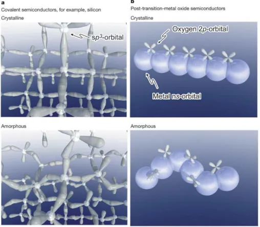
As a solution to the problem of amorphous semiconductors, H. Hosono et al reported the exploration guidelines for ionic amorphous oxide semiconductors (AOSs) in 1996 [13]. According to the report, the low mobility of a-Si:H is explained by a model of the carrier transport paths (that is, the wave-function of the conduction band bottom); covalent semiconductors such as a-Si:H have average carrier transport paths composed of strongly directive sp3 orbitals, so structural randomness of amorphous greatly degrades the magnitude of bond overlap, that is, carrier mobility (Figure 1-1(a)). In contrast, the conduction band bottom in the oxide semiconductors containing of post-transition-metal
3
cations is primarily composed of spatially spread metal ns orbitals with isotropic shape (n is the principal quantum number), and direct overlap among the neighboring metal ns orbitals is rather large (Figure 1-1(b)). The magnitude of this overlap is not significantly affected even in an amorphous structure, therefore, AOSs exhibit large mobilities similar to those of the corresponding crystalline phase (~ 10 cm2 V-1s-1) [13, 14]. In other words, although the mobilities of the crystalline oxide semiconductors (~100 cm2V-1s-1) is inferior to that of crystalline silicon (~1500 cm2V-1s-1), in the case of amorphous, AOSs have the potential to give high mobilities (~10 cm2V-1s-1) exceeding the value of a-Si:H (~0.1 cm2V-1s-1).
H. Hosono et al. demonstrated new materials, amorphous Cd2GeO4, AgSbO3 and
Cd2PbO4, on the basis of this guideline [13], then, the novel AOS a-In-Ga-Zn-O
(a-IGZO) was reported in Nature by same group in 2004. This report of the a-IGZO deposited at room temperature demonstrated distinctive features of AOSs: (i) high electron mobility (≥10 cm2
V−1s−1), including the field-effect mobility, and (ii) control of carrier density over a broad range from <1014 to 1020 cm−3 [15]. Since then, and up to the present, AOSs such as a-IGZO have been extensively studied as promising semiconductors for thin-film transistors (TFTs) in drive circuits for large-size and/or high-resolution liquid crystal displays (LCDs) and organic light emitting diode (OLED) displays [16, 17, 18].
Another advantage of AOSs is the ability to significantly and controllably tune their physical properties over a wide range by large variations in their composition. This is enabled by the much higher solubility limit of the amorphous phase relative to that of the solid crystalline phase. For example, AOS band gap energies have been modified through compositional variations from 2.66 to 3.05 eV in the In–Zn–O system [19], from
4
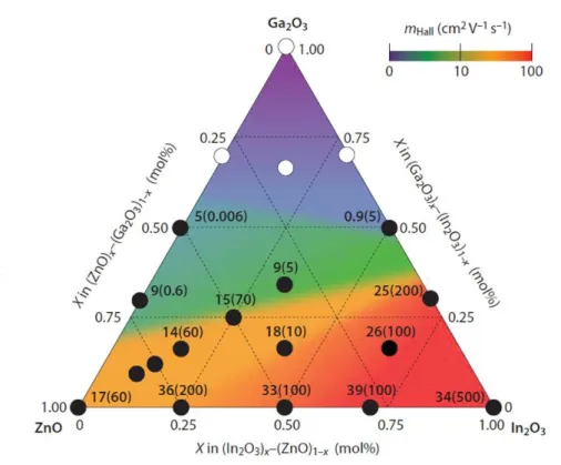
3.8 to 4.9 eV in the Zn–Ga–O system [20], and from 3.1 to 4.4 eV in the Cd–Ge–O system [21]. Carrier density and Hall mobility in the Hf–In–O system change from 1016 to 1019 cm–3 and from 16.6 to 6.53 cm2V–1s–1, respectively [22]. Furthermore, Nomura et al. demonstrated the variations in the composition-dependent electrical properties of amorphous ternary In2O3–ZnO–Ga2O3 system (Figure 1-2) [23].
These features indicating that the applicability of AOSs is not only for TFTs. Although the band gap of a-IGZO is 3.1 eV, if the band gap can be narrowed down to ~2.5 eV while maintaining the electric characteristics, it can be applied to a solar cell capable of absorbing the strongest wavelength range of sunlight. In addition, very wide bandgap AOSs (≥4.1 eV) (Fig. 1-3) may also find applications in solar-blind UV detectors such as flame detectors [24]. Since most of devices such as displays are used under light irradiation, this feature is also meaningful for those applications. Broader optoelectronic applications of AOSs are expected by realizing band gap control of AOSs while maintaining electrical properties.
Potentials of AOS for optoelectronic applications
Optoelectronic applications using oxide semiconductors have been studied so far. For example, solar cells with wide bandgap semiconductors, such as oxides, are expected to display high open circuit voltages (Vocs). A theoretical analysis of a triple-junction
solar cell has predicted energy conversion efficiencies surpassing 20% using a 2.0 eV-bandgap semiconductor as a top cell photovoltaic material [25], prompting extensive research on oxide solar cells such as n-type ZnO/p-type Cu2O cells [26-28]. Although
5
[29], and no application has appeared to date. In recent studies, conversion efficiencies of 8.1% in n-type Zn1-XGeX-O /p-type Cu2O solar cells was reported [30], however, this
value is still insufficient for practical use.
The low energy conversion efficiencies of oxide solar cells are due to the problems of heterojunction. In oxide semiconductors, there are very few bipolar semiconductors that have carrier type controllability. Therefore, heterojunctions are inevitably formed in the fabrication of electronic devices by using oxide semiconductors. In the case of heterojunction, there are two problems. The first problem is caused by difference in crystal structures between p-type material and n-type material. The junction between materials with different crystal structures causes to generation of defects at the junction interface, leading to a performance degradation. The second problem is caused by difference in band structures between p-type material and n-type material. The discontinuity of the band due to the difference in the positions of the band edges between two materials causes the performance deterioration. Therefore, the energy positions of the conduction band minimum (CBM) and the valence band maximum (VBM) are important parameters for heterojunction device design. Band alignment of the ZnO / Cu 2 O system is shown in Figure 1-4. In this system, small difference of the
Fermi level (0.9 eV), i.e. low open circuit voltage, is also considered to limit the conversion efficiency.
In response to these problems, generation of defects at the junction interface can be suppressed by using AOSs which have no crystal structure in one side of the p-n junction. Furthermore, discontinuity of the band due to the difference in the band edges could be improved by the band edge control of the AOSs. Therefore, I thought that the material design and band gap control of AOS in consideration of the band edge position could
6
solve the problem of heterojunction. If the control of the band gap and the band edge position of AOSs over a wide range while maintaining high mobility in one material system are realized, it is expected that preparation of electronic devices by selecting the optimum composition according to the applications and joined materials is possible, without severe optimization of process conditions.
7
Fig. 1-1 Schematic orbital models for the carrier transport paths (i.e. conduction band
bottoms) in crystalline and amorphous semiconductors described in Nature 432, 488 (2004) by K. Nomura et al. (a) show the carrier transport paths of Covalent semiconductors which composed of strongly directive sp 3 orbitalsty. (b) is the case of amorphous oxide semiconductors composed of post-transition-metal cations. Spheres denote metal s orbitals, and the contribution of oxygen 2p orbitals is small.
8
Fig. 1-2 The carrier mobilities and concentrations for the amorphous thin films in the
In2O3–Ga2O3–ZnO system described in Jpn. J. Appl. Phys. 45, 4303 (2006) by K.
9
Fig. 1-3 Spectral irradiance of sunlight on the ground. The bandgap energies of a-IGZO
(Eg = 3.1 eV) are large for the active layer of solar cells (~ 2.5 eV) and small for
10
11 Objectives of present study
Taking the backgrounds into consideration, the target formulated in the present study is to propose and demonstrate a new material system that can realize band gap variable n type AOS with electrical characteristics applicable to optoelectronic devices. In order to realize this target, I gave four objectives as follows.
(1) Proposal of material design guidelines for AOS that can achieve band gap tunability and electrical characteristics applicable to optoelectronic devices.
(2) Demonstration of band gap variable AOS with high mobility by preparation of amorphous thin film in selected material system.
(3) Demonstration of band edge control: proposal of the optimal composition of the new AOS films assuming the p-n junction with p-Cu2O.
(4) Improvement of electrical properties of the new AOS films by post-deposition treatment.
12
Outline of the present study
This thesis consists of six chapters.
In chapter 1, current status of amorphous oxide semiconductors was summarized, and
the significance of band gap variable AOS exploration for optoelectronic applications and the objective of present study were described.
In chapter 2, material design for demonstrating band gap tunable AOS with electrical
properties applicable to optoelectronic applications was proposed, and candidate materials were selected.
In chapter 3, thin film of the system combining selected candidate materials, CdO and
second components of Al, Si, and Ga, were prepared by radio frequency sputtering method, respectively, and the conditions for the amorphous film and composition controllability were investigated.
In chapter 4, band gap control of amorphous Cd-Ga-O system which gave positive
results in Chapter 3 was investigated and band alignment was evaluated assuming the p/n junction with Cu2O.
In Chapter 5, post-deposition annealing was conducted to improve the electrical
properties of amorphous Cd-Ga-O films.
13 References
[1] Taur, Y. and Ning, H. T., Fundamentals of Modern VLSI Devices, Cambridge Univ. Press, New York (1988).
[2] Kuo, Y., Thin Film Transistors: Materials and Processes, Kluwer Academic, Dordrecht (2004).
[3] H. E. A. Huitema, G. H. Gelinck, J. B. P. H. van der Putten, K. E. Kuijk, C. M. Hart, E. Cantatore, P. T. Herwig, A. J. J. M. van Breemen and D. M. de Leeuw, Nature
414, 599 (2001).
[4] N.F. Mott and E.A. Davis, Electronic Processes in Non-Crystalline Materials, Clarendon, (1979).
[5] E.P. Denton, H. Rawson, and J.E. Stanworth, Nature 173, 1030 (1954). [6] N. A. Goryunova and B. T. Kolomiets, J. Tech. Phys. 25, 984 (1955). [7] S. R. Ovshinsky, Phys. Rev. Lett. 21, 1450 (1968)
[8] W.E. Spear and P.G. LeComber, Solid State Commun. 17, 1193 (1975).
[9] Kagan, C. R. and Andry, P., Thin Film Transistors, Marcel Dekker, New York (2003).
[10] C.-S. Yang, L. L. Smith, C. B. Arthur, and G. N. Parsons, J. Vac. Sci. Technol. B 18, 683 (2000).
[11] Paul G. Carey, Patrick M. Smith, Steven D. Theiss, and Paul Wickboldt, J. Vac. Sci.
Technol. A 17, 1946 (2000).
[12] S.-C. Wang, C.-F. Yeh, C.-K. Huang and Y.-T. Dai, Jpn. J. Appl. Phys. 42, 1044 (2003).
[13] H. Hosono, N. Kikuchi, N. Ueda, and H. Kawazoe, J. Non-Cryst. Solids 198–200, 165 (1996).
14
[14] M. Orita, H. Ohta, and M. Hirano, Phil. Mag. B 81, 501 (2001).
[15] K. Nomura, H. Ohta, A. Takagi, T. Kamiya, M. Hirano, and H. Hosono, Nature 432, 488 (2004).
[16] T. Kamiya, K. Nomura and H. Hosono, Sci. Technol. Adv. Mater. 11 (2010). [17] D. S. Ginley, H. Hosono, and D. C. Paine, Handbook of Transparent Conductor,
Springer, New York, (2010).
[18] P. Barquinha, R. Martins, L. Pereora and E. Fortunato, Transparent Oxide Electronics, Wiley,Chichester, (2012).
[19] B. Kumar, H. Gong, and R. Akkipeddi, J. Appl. Phys. 98, 073703 (2005).
[20] J. Zhao, X. W. Sun, and S. T. Tan, IEEE Trans. Electron. Devices 56, 2995 (2009). [21] N. Kikuchi, H. Hosono, H. Kawazoe, K. Oyoshi, and S. Hishita, J. Am. Ceram. Soc.
80 ,22 (1997).
[22] C. Kim, S. Kim, J. Lee, J. J. Park, S. Kim, J. Park, E. Lee, Y. Park, J. H. Kim, S. T. Shin and U. Chung, Appl. Phys. Lett. 95, 252103 (2009).
[23] K. Nomura, A. Takagi, T. Kamiya, H. Ohta, M. Hirano, and H. Hosono, Jpn. J. Appl.
Phys. 45, 4303 (2006).
[24] T. Oshima, T. Okuno, N. Arai, N. Suzuki, H. Hino, and S. Fujita, Jpn. J. Appl. Phys.,
48, 011605 (2009).
[25] I. A. Yunaz, A. Yamada, and M. Konagai, Jpn. J. Apll. Phys., 46, L1152 (2007). [26] A. Mittiga, E. Salza, F. Sarto, M. Tucci, R. Vasanthi, Appl. Phys. Lett., 88, 163502
(2006).
[27] T. Minami, Y. Nishi, T. Miyata, and J. Nomoto, Appl. Phys.Exp., 4, 062301 (2011). [28] K. Lee, K. Nomura, H. Yanagi, T. Kamiya, H. Hosono, Electrochem. Solid-State
Lett., 14, H346 (2011).
[29] T. Minami, Y. Nishi, and T. Miyata, Appl. Phys. Exp. 8, 022301 (2015). [30] T. Minami, Y. Nishi, and T. Miyata, Appl. Phys. Exp. 9, 052301 (2016).
15
16
Chapter 2. Material design
Introduction
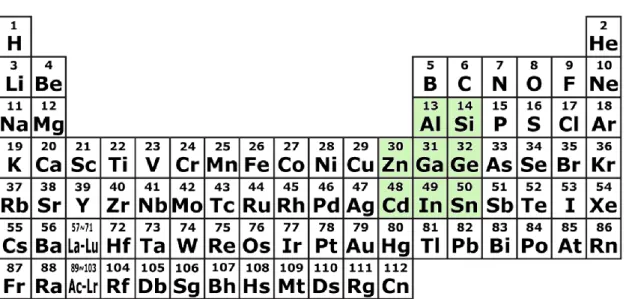
According to the exploration guidelines for amorphous oxide semiconductors reported by H. Hosono et al, high mobility of AOS such as a-IGZO is originated from the conduction band minimum primarily composed of spatially spread metal ns orbitals with isotropic shape (n is the principal quantum number) [1]. The magnitude of direct overlap among the neighboring metal ns orbitals is insensitive to distorted chemical bonds that intrinsically exist in amorphous materials [2, 3]. In addition, to maintain the transmittance for optoelectronic applications, transition metals which have closed-shell electronic structure were eliminated, therefore metal ions below whose oxides' conduction band minimums formed by cation ns0 orbitals were candidates (n = 3 for Al3+, Si4+; n = 4 for Zn2+, Ga3+, Ge; and n = 5 for Cd2+, In3+, Sn4+) (Figure 2-1).
In this chapter, constitutional elements to demonstrate band gap tunable AOS with high mobility for optoelectronic applications were considered from these candidates.
17
Fig. 2-1 The candidate material to obtain high carrier mobility were ishown by green.
Because high mobility of AOS is originated from the conduction band minimum primarily composed of spatially spread metal ns orbitals with isotropic shape (n is the principal quantum number), metal ions whose oxides' conduction band minimums formed by cation ns0 orbitals (n = 3 for Al3+, Si4+; n = 4 for Zn2+, Ga3+, Ge; and n = 5 for Cd2+, In3+, Sn4+) were candidate.
18 Materials selection
The constitutional materials to realize high-mobility n-type AOSs presenting band gap energies tunable for solar cells (ca. 2 eV) and solar-blind devices (≥4.1 eV) were considered based on four factors below.
First, the combination to realize widely bandgap-tunability was considered. The combination of two materials with extremely different bandgap energy is suitable for bandgap control over a wide range by varying the chemical compositions. The bandgap energies of candidate oxides are shown in figure. 2-2. The bandgap energy of CdO (Eg
= 2.2 eV [12]) is obviously small compared to other candidate oxides. Therefore, Cd was selected as the first constitutional element. Second materials were selected in wide bandgap oxide. Wider bandgap oxides are suitable as Second materials. Thus, I focused on three candidates of Al2O3 (Eg = ~ 8.8 eV [4, 5, 6]) and SiO2 (8.4 eV [7]) and Ga2O3
(4.7 eV [10]) with largest bandgap energy.
Second, crystal structures of constitutional materials also should have considered. Since the CdO has an NaCl type crystal structure, CdO it is easily crystallized, even when deposited at room temperature. I considered that the combination of the second component with significantly different crystal structure was important to realize an amorphous phase in the cadmium-oxide system. As shown in Fig.2-3, three candidates of Al2O3 and SiO2 and Ga2O3 have completely different structure from that of
NaCl-type structure. Therefore, it is expected that adding these second components effectively play the role as a stabilizing additive to maintain the amorphous structure in wade composition range and wide temperature range in Cd-O system.
19
carrier electrons, making carrier density difficult to control in many conducting oxides such as CdO. Therefore, it is necessary to suppress generation of excessive oxygen vacancy in order to control the carrier concentration. Adding the ion species having strong binding energy with oxygen, such as Ga3+, Al3+, is considered effective to suppression of oxygen vacancy. Also in the case of In-Ga-Zn-O, Ga3+ is known to play a role as a carrier inhibitor [16, 17].
Fourth, materials for high mobility were considered. The carrier transport paths (i.e. the conduction band bottom) in the oxide semiconductors is primarily composed of spatially spread metal ns orbitals with isotropic shape (n is the principal quantum number). The magnitude of direct overlap among the neighboring metal ns orbitals are linked to the magnitude of mobility. Therefore, a system containing heavy metal ions with large ns orbital spread (i.e. n > 5) is suitable for demonstration of AOS with high mobility. The conduction band bottom of CdO containing Cd2+, which is a typical heavy metal ion, is composed of Cd2+ 5s0 orbitals, satisfies the condition for high mobility.
20
Fig. 2-2 The bandgap energies of candidate oxides [4-15]. The combination of two
materials with extremely different bandgap energy is suitable for bandgap control over a wide range by varying the chemical compositions.
21
22 Conclusion
The CdO-Al2O3, CdO-SiO2, and CdO-Ga2O3 systems were selected as a possible
candidate to realize high-mobility n-type AOSs presenting bandgap energies tunable for solar cells (ca. 2 eV) and solar-blind devices (≥4.1 eV), based on several factors below. (i) The conduction band minimums (CBMs) of oxides mainly consist of cation ns0 orbitals (n = 3 for Al3+ and Si4+; n = 4 for Ga3+; and n = 5 for Cd2+), and this electronic configuration is suitable for high-electron-mobility AOSs. (ii) Bandgap energies significantly differ between CdO (Eg = 2.2 eV) and the others (Eg = 8.7 eV for Al2O3,
8.4 eV for SiO2, and 4.7 eV for Ga2O3). (iii) Second component such as Al2O3, SiO2,
and Ga2O3 may play an important role in stabilizing an amorphous structure and
23 Reference
[1] K. Nomura, H. Ohta, A. Takagi, T. Kamiya, M. Hirano, and H. Hosono, Nature 432, 488 (2004).
[2] Mott, N. F., Adv.hys. 26, 363–391 (1977).
[3] S. Narushima, M. Orita, M. Hirano, and H. Hosono, Phys. Rev. B 66, 35203 (2002). [4] E. T. Arakawa and M. W. Williams, J. Phys. Chem. Solids 29 735, (1968).
[5] M. E. Innocenzi, R. T. Swimm, M. Bass, R. H. French, A. B. Villaverde, and M. R. Kokta, J. Appl. Phys. 67 7542, (1990).
[6] D. F. Heath and P. A. Sacher, Appl. Optics 5 937 (1966).
[7] Edward D. Palik, Handbook of Optical Constants of Solids vol.1 719 (1997) [8] T. Minami, H. Nanto, and S. Takata, Appl. Phys. Lett., 41, 1968 (1982) [9] T. Minami, H. Nanto, and S. Takata, Jpn. J. Appl. Phys., 24, L851 (1985)
[10] N. Ueda, H. Hosono, R. Waseda, and H. Kawazoe, Appl. Phys. Lett., 71, 933 (1997) [11] N. Ueda, H. Maeda, H. Hosono, and H. Kawazoe, Jpn. J. Appl. Phys., 84, 6174
(1998)
[12] X. M. Ding L. M. Hung, L. F. Cheng, Z. B. Deng, X. Y. Hou, C. S. Lee, and S. T. Lee, Appl. Phys. Lett., 76, 2704 (2000)
[13] R. Banerjee, D. Das, Thin Solid Films, 149, 291 (1987)
[14] T. Ishida, O. Tabata, J. Park, S. H. Shin, H. Magara, S. Tamura, S. Mochizuki, T. Mihara, Thin Solid Films, 281, 228 (1996)
[15] H. S. Randhawa, M. D. Matthews, and R. F. Bunshah, Thin Solid Films, 83, 267 (1981)
[16] M. Oruta, H. Ohta, M. Hirano, S. Narushima, and H. Hosono, Phil. Mog. B. 81, 501 (2001)
24
[17] K. Nomura, A. Takagi, T. Kamiya, H. Ohta, M. Hirano, and H. Hosono, Jpn. J. Appl.
25
Chapter 3. Exploration of preparation conditions for new
AOSs: Cd-Al-O, Cd-Si-O, and Cd-Ga-O
Introduction
Amorphous oxide semiconductors (AOSs), such as amorphous In–Ga–Zn–O (a-IGZO) [1] are one of the most promising materials for thin-film transistors (TFTs) in the next-generation flat-panel displays [2]. In particular, a-IGZO exhibits high mobility (≥10 cm2V−1s−1) and controllable carrier density ranging from less than 1014 to 1020cm−3[1]. These features indicate that AOSs present low defect densities, making them attractive for TFTs and other semiconductor devices such as solar cells and ultraviolet (UV) detectors. However, the bandgap energies (Eg) of a-IGZO (3.0–3.2 eV
for In/Ga/Zn¼1:1:1) are significantly large for the active layer of solar cells and very small for solar-blind devices. Bandgap energies of AOSs have been modulated from 3.1 to 4.4 eV in the Cd–Ge–O system [3], from 3.8 to 4.9 eV in the Zn–Ga–O system [4], and from 2.66 to 3.05 eV in the In–Zn–O system [5]. However, these bandgaps did not simultaneously cover the ranges required for solar cells and solar-blind devices. In addition, electron transport properties were unsuitable for high-speed semiconductor devices. The mobility of a-Zn–Ga–O was significantly small (ca. 10−1cm2V−1s−1), whereas the carrier density of a-In–Zn–O was significantly high (more than 1020cm−3).
The constitutional materials to realize band gap variable n type AOS with electrical characteristics applicable to optoelectronic devices were discussed in chapter 2, and the CdO-Al2O3, CdO-SiO2, and CdO-Ga2O3 systems were selected as a possible
candidate. In this chapter, I tried to fabricate amorphous film of these systems by sputtering method. These combinations contained CdO are expected to display good
26
mobility. However, CdO is easily crystallized because of their simple crystal structure of NaCl type. Hence, preparation conditions to obtain the amorphous films were investigated.
Experimental
Preparation of Sputtering targets
The CdO target were prepared by high-temperature solid phase reaction method. CdO powder (Kojundo Chemical Laboratory Co., Ltd., 99.99%) was put into die and uniaxial pressed at 100 MPa. Compacted pellet was sintered at 1000 °C for 8hours, single-phase sintered compact of CdO was obtained. Similarly, Ga2O3 target was
prepared by sintering of pressed Ga2O3 powder (Kojundo Chemical Laboratory Co., Ltd.,
99.9%) at 1500 °C for 9 hours. In the case of Al2O3 and SiO2, commercial targets
(Kojundo Chemical Laboratory Co., Ltd., 99.9% and Toshima Manufacturing Co., Ltd., 99.99%) were employed.
Preparations and characterizations of Cd-Al-O and Cd-Si-O films
Cd-Al-O films and Cd-Si-O films were deposited on silica glass substrates (Kobayashi-Special Glass Co., Ltd., 10 mm ×10 mm×1 mm) at room temperature by radio-frequency (RF) magnetron sputtering method. Sintered CdO, Al2O3, and SiO2 were
used as the sputtering targets. Details of sputtering conditions are summarized in Table
27
10 W - 40 W, 5 W - 10 W were set to examine the conditions for amorphous film. Sputtering conditions are summarized in Table 3-I. Film structures were examined by X-ray diffraction (XRD) (Cu Kα, Rigaku Rint-2500).
Table 3-I. Sputtering conditions for Cd-Al-O and Cd-Si-O films
Target CdO Al2O3 or SiO2
Substrate SiO2 glass
Substrate temperature RT (w/o intentional heating) RF power (W) 5, 10 50 Process gas Ar (99.999%) Process pressure (Pa) 1.5, 5 Gas flow rate (sccm) 10
Preparations and characterizations of Cd-Ga-O
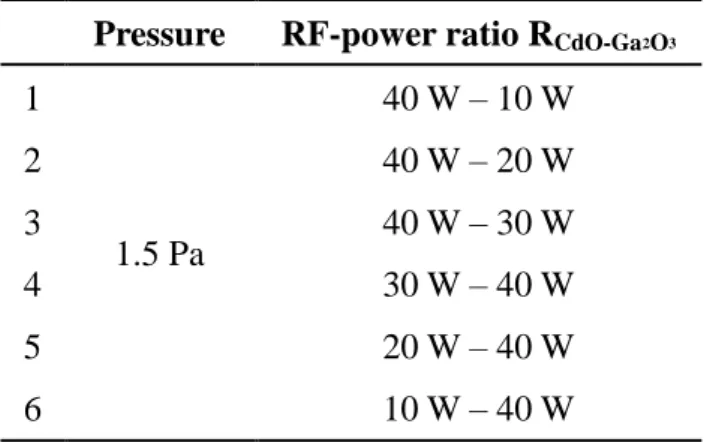
Cd-Ga-O films were deposited on silica glass substrates (Kobayashi-Special Glass Co., Ltd., 10 mm ×10 mm×1 mm) at room temperature by radio-frequency (RF) magnetron sputtering similar to Cd-Al O and Cd-Si-O. Ar (99.999%) was used as the sputtering gas, and sputtering pressure was set at 1.5Pa. RF-power ratio (RCdO-Ga2O3) were
varied from 10 W - 40 W to 40 W - 10 W. Sputtering conditions are summarized in Table
3-Ⅱ.
Film structures were examined by X-ray diffraction (XRD) (Cu Kα, Rigaku Rint-2500). The chemical compositions of films were measured by wavelength-dispersive X-ray fluorescence spectroscopy (WD-XRF) (Rigaku ZSX Primus II) using CCd = [Cd]/([Cd] + [Ga]). Optical transmission (T) in the
28
UV-visible-near infrared region were recorded by spectrophotometer (Shimadzu UV-3600), estimated the optical bandgap energies (Eg). Electrical conductivities were
measured by digital multimeter (Keithley 2400)
Table 3-Ⅱ. Sputtering conditions for Cd-Ga-O
Pressure RF-power ratio RCdO-Ga2O3
1 1.5 Pa 40 W – 10 W 2 40 W – 20 W 3 40 W – 30 W 4 30 W – 40 W 5 20 W – 40 W 6 10 W – 40 W
29 Results and discussion
Cd-Al-O and Cd-Si-O
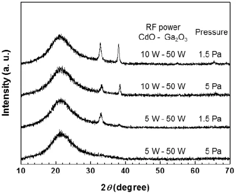
Figure 3-1 shows typical glancing angle XRD patterns of Cd-Al-O films deposited
each conditions. A broad peak detected around 22° was attributed to the silica glass substrates. In the XRD pattern of films deposited at 5 Pa and RCdO-Al2O3 of 5 W - 50W, no
sharp peak attributable to a crystalline phase was observed, indicating that obtained film was amorphous. However, in the XRD patterns of films deposited at the RF-power ratio RCdO-Al2O3 of 10 W - 50W, distinct peaks were observed around 32° and 38°, which
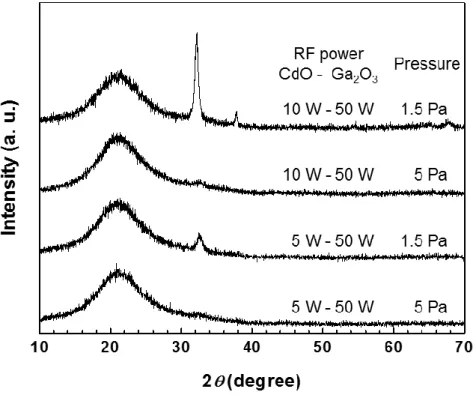
attributed the first and second strongest peak of crystalline CdO with NaCl-type crystal structure. The film deposited at low pressure of 1.5 Pa was also crystal, even the RF-power ratio of CdO was low (RCdO-Al2O3 of 5 W - 50W). As shown in Figure 3-2,
similar dependence was observed in the case of Cd-Si-O. Only the condition with 1.5 Pa and RCdO-SiO2 of 5 W - 50W provide amorphous Cd-Si-O film. Further increasing of
sputtering pressure could be effective to obtain amorphous structure. However, increasing of sputtering pressure decrease dramatically the sputtering speed.
30
Fig. 3-1. Glancing angle XRD patterns of Cd-Al-O films prepared by the varied
31
Fig. 3-2. Glancing angle XRD patterns of Cd-Si-O films prepared by the varied
32 Cd-Ga-O
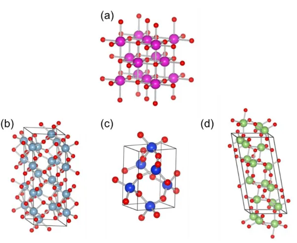
Figure 3-3 shows typical glancing angle XRD patterns of obtained Cd-Ga-O films.
No distinct peak attributable to a crystalline phase was observed in XRD patterns of any obtained films except a film deposited at highest CdO Rf-power ratio of 40 W – 10 W. Therefore, Cd-Ga-O films were obtained by all conditions listed in Table 3-Ⅱ except the RCdO-Ga2O3 of 40 W – 10 W, demonstrating that Ga effectively plays the role as a
stabilizing additive to maintain the amorphous structure. In addition, chemical compositions of obtained films were estimated by XRF measurements. The Cd concentration of the films (Cd/(Cd+Ga)) was increased from 32% to 45% by varying the RCdO-Ga2O3from 40 W – 10 W to 10 W – 40 W.
Figure 3-4 shows optical transmission spectra of obtained films. All the films
displayed T values greater than 90% in the near infrared region. Inset shows the extended transmittance spectra around absorption edges. The red-shift at the absorption edge was observed by increasing the Cd concentration. The optical bandgap energies (Eg) of all obtained a-CGO films were estimated using the Tauc plot [1]. Figure 3-5
shows the chemical composition-dependent Eg. Eg values decreased from 3.9 to 3.5 eV
when CCd increased from 32 to 45 %, indicating that the variations in film’s chemical
composition enable control Eg of amorphous Cd-Ga-O.
Electrical conductivities of obtained films were investigated. Figure 3-6 shows the composition dependence of electrical conductivities. The values of electrical conductivities were increased by increasing Cd concentration in the films. In the case of relatively low Cd concentration film, measurable values were not obtained because of their low conductivities (< 10–6 Scm–1) The small electrical conductivities of low Cd concentration film could be explained by the smaller dispersion of Ga 4s orbital relative
33
to that of Cd 5s and the weaker hybridization between the s orbitals in a low-Cd film relative to high-Cd films.
Fig. 3-3. Glancing angle XRD patterns of Cd-Ga-O films. Chemical compositions
34
Fig. 3-4. Optical transmission spectra of Cd-Ga-O films. The inset shows the extended
35
Fig. 3-5. Optical bandgaps (Eg) estimated using Tauc plots as a function of film chemical
36
37 Conclusions
Cd-Al-O, Cd-Si-O, and Cd-Ga-O films were prepared by RF-sputtering method. Amorphous films of Cd-Al-O and Cd-Si-O were obtained on the annealing conditions with 1.5 Pa and RCdO-Al2O3, RCdO-SiO2 of 5 W – 50 W. In contrast, in the case of Cd-Ga-O,
widely range of RCdO-Ga2O3 ratio provided amorphous films. Compare to Al and Si, Ga
plays the role more effectively as a stabilizing additive to maintain the amorphous structure. The chemical compositions of the films (Cd/(Cd+Ga)) were shifted from 32 to 45 % were by varying the RCdO-Ga2O3 ratio, band gap energies were changed from 3.9 to
3.5 eV. However, film with highest Cd/(Cd+Ga) value of 45 % (Eg = 3.5 eV) was not
single-phase amorphous Cd-Ga-O, CdO poly-crystalline phase was contained. Composition dependence of electrical properties were observed, but the films with low Cd/(Cd+Ga) value of 32 % and 33 % (Eg = 3.9 and 3.8 eV, respectively) were insulator.
Therefore, unfortunately, controlled band gap energy range which maintained the amorphous structure was small (Eg = 3.9 to 3.6 eV). However, these results suggested a
possibility for wider range band gap tunability by further varying the film composition in Cd-Ga-O system.
38 References
[1] K. Nomura, H. Ohta, A. Takagi, T. Kamiya, M. Hirano, and H. Hosono, Nature, 432, 488 (2004).
[2] D. S. Ginley, H. Hosono, and D. C. Paine, Handbook of Transparent Conductor (Springer, New York, 2010).
[3] N. Kikuchi, H. Hosono, H. Kawazoe, K. Oyoshi, and S. Hishita, J. Am.Ceram. Soc.
80, 22 (1997).
[4] J. Zhao, X. W. Sun, and S. T. Tan, IEEE Trans. Electron. Devices 56, 2995 (2009). [5] B. Kumar, H. Gong, and R. Akkipeddi, J. Appl. Phys. 98, 073703 (2005)
39
Chapter 4. Band-gap control in amorphous Cd-Ga-O Thin
Films
Introduction
In chapter 4, high-mobility n-type AOSs presenting bandgap energies tunable for solar cells (ca. 2 eV) and solar-blind devices (≥4.1 eV) were investigated by focusing on the CdO-Ga2O3 system. In Chapter3, film composition of a-Cd-Ga-O was varied by Rf
power ratio. However, the variation of the composition was limited from 30% to 45%. This is due to the difference in sputtering rate between CdO and Ga2O3. Therefore, other
method to control the film compositions was considered. Instead of two sputtering targets using a sintered body of CdO and Ga2O3, sputtering system using a mixture of CdO and
Ga2O3 powder was employed. I tried to control the film compositions by varying the
mixing ratio of powder target.
In addition, oxygen vacancies often generate carrier electrons, making carrier density difficult to control in many conducting oxides such as CdO. Hence, film preparation conditions were optimized to obtain bandgap tunable amorphous Cd-Ga-O (a-CGO) films exhibiting high mobility (ca. 10 cm2V−1s−1). The energy positions of the CBM and the valence band maximum (VBM), which are important parameters for heterojunction device design, were measured by UV photoemission spectroscopy (UPS).
40 Experiment
Preparation of a-CGO films
The a-CGO films were deposited on silica glass substrates (Kobayashi-Special Glass Co., Ltd., 10 mm ×10 mm×1 mm) at room temperature by radio-frequency (RF) magnetron sputtering method. The substrate holder head was cooled with circulating water to prevent unintentional elevation of substrate temperature. Compacted CdO (Kojundo Chemical Laboratory Co., Ltd., 99.99%) and β-Ga2O3 (Kojundo Chemical
Laboratory Co., Ltd., 99.9%) mixed powders were employed as sputtering targets: the mixed powder was set in a 2-inch diameter aluminum dish on the sputtering source. Film compositions were tried to control by continuously varying the CdO:Ga2O3 ratio
of the powder target (RCdO/Ga2O3) from 6:1 to 2:3. The RF power was set to 50 for
RCdO/Ga2O3 values ranging between 6:1 and 2:1, 100 W for Ga2O3 content of 50%
(amounting to RCdO/Ga2O3 values of 1:1) or over, respectively, because the deposition rate
decreased dramatically when the Ga2O3 content increased in the targets. Optimized
sputtering conditions are summarized in Table 4-I.
Table 4-I. Optimized sputtering conditions for a-CGO thin films.
Target CdO-Ga2O3 mixture powder
Molar ratio (CdO:Ga2O3) 6:1-2:1 1:1-2:3
Substrate SiO2 glass
Substrate temperature RT (w/o intentional heating) RF power (W) 50 100 Process gas Ar (99.999%)
Process pressure (Pa) 2.5 Gas flow rate (sccm) 10
41 Characterization
Film structures were examined by X-ray diffraction (XRD) (Cu Kα, Rigaku Rint-2500) and transmission electron microscopy (TEM) (FEI Tecnai Osiris). The Cd content in the films was measured by wavelength-dispersive X-ray fluorescence spectroscopy (WD-XRF) (Rigaku ZSX Primus II) using CCd = [Cd]/([Cd]+[Ga]) [1].
Optical transmission (T) and reflectance (R) spectra in the UV-visible-near infrared region were recorded by spectrophotometer (Shimadzu UV-3600), estimated the optical bandgap energies (Eg). To obtain optical absorption coefficients (α), the effect of the
interference fringes was removed and the reflectance correction was performed using
T/(1–R) = exp(–αd), where d is the film thickness. Carrier transport properties were
evaluated by Hall measurements according to the van der Pauw method (Toyo Corporation Resitest 8300). Ionization potentials were determined by in situ UV photoemission spectroscopy (UPS) measurements to estimate the energy positions of the conduction band minimums (CBM) and the valence band maximum (VBM).
Results and discussion
Compositions and structures
XRF measurements provided wide range of CCd values of obtained films from 79 %
to 18 %, indicating that film compositions of a-CGO were continuously controlled from ~80 % to ~20 % by varying the RCdO/Ga2O3 ratios from 6:1 to 2:3.
Figure 4-1 shows typical glancing angle XRD patterns of the three typical obtained
42
(33%) Ccd values. Hereafter, a-CGO films with CCd of ~80%, ~50%, and ~30% were
referred to as Cd80, Cd50, and Cd30, respectively. A broad peak detected around 22° was attributed to the silica glass substrates, as confirmed by the substrate XRD pattern (top graph). On the other hand, another peak observed around 32° which is the same peak position as the strongest peak of crystalline CdO, was assigned to the films. Crystalline CdO has NaCl-type crystal structure, which is the close-packed structure of the edge sharing CdO6 octahedra. I assume that distorted CdO6 octahedral short-range structures
and the edge sharing networks by the octahedra would remain in the amorphous a-CGO. Therefore, the XRD broad peak of a-CGO is observed at almost same position to the strongest peak of crystalline CdO. A decrease in Cd concentration reduced the peak intensity because Cd has a larger atomic number (Z = 48) than Ga (Z = 31), resulting in larger X-ray scattering cross-section. No sharp peak attributable to a crystalline phase was observed in XRD patterns of any obtained films. Therefore, all the films prepared by the conditions listed in Table I were considered to be amorphous. On the other hand, films prepared using pure CdO powder targets were polycrystalline, demonstrating that a stabilizing additive is required to maintain the amorphous structure; Ga effectively plays this role.
TEM observations were conducted to exclude the potential existence of nanocrystals. Figure 4-2 shows the electron beam diffraction of a Cd50 film. Halo rings without diffraction spots were observed. A dark-field image of the halo ring indicated by an arrow in Fig. 4-2. (a) showed a bright contrast for the film and confirmed that this ring originated from the film (Fig. 4-2. (b)). Tilting the sample did not change the granular structure contrast. In addition, similar results were obtained when these measurements were repeated in different areas, indicating that the obtained thin films
43
were not mixture of a-CGO and any crystalline phase including crystalline CdO. Moreover, the chemical composition of same Cd50 film was analyzed by energy-dispersive X-ray (EDX) mapping. Figure 4-3. (a) shows the High-angle annular dark field (HAADF) image of scanning TEM, and EDX mapping of Cd (Fig. 4-3. (b)) and Ga (Fig. 4-3. (c)) in this area were observed. As shown these figures, the Cd and Ga concentrations were uniform over the films.
44
Fig. 4-1. Glancing angle XRD patterns of a-CGO films whose Cd/(Cd+Ga) are ~80,
45
Fig. 4-2. (a) Electron diffraction and cross-sectional TEM images of a-CGO film
(Cd/(Cd+Ga) = ~50%). (b) A dark-field image from the halo ring indicated by an arrow in (a).
46
Fig. 4-3. The chemical composition of a-CGO film (Cd/(Cd+Ga) = ~ 50%) by EDX. (a)
47 Optical properties
Figure 4-4 shows optical transmission spectra of Cd80, Cd50, Cd20 films (t = ~
50 nm). These values were corrected for the substrate reflection/absorption used as a reference. All the films displayed T values greater than 90% in the near infrared region. In addition, the red-shift at the absorption edge was clearly observed by increasing the Cd concentration. The optical bandgap energies (Eg) of all obtained a-CGO films were
estimated using the Tauc plot [2]. Fig. 4-5 shows the chemical composition-dependent
Eg values. Eg values increased from 2.3 to 4.5 eV when CCd decreased from 79 to 18%,
indicating that the variations in film’s chemical composition enable control over Eg in a
wide range.
Fig. 4-4. Optical transmission spectra of a-CGO films (Cd/(Cd+Ga) = ~80, ~50, and
48
Fig. 4-5. Dependence of optical band gaps (Eg) estimated by using Tauc’ plots on
49 Electrical properties
Figure 4-6 shows the electrical conductivity (σ), carrier density (N), and Hall
mobility (μ) of the films as functions of Ccd at RT. All the films showed negative Hall
voltages, which is consistent with their n-type conductivity.
The relatively high N values obtained for the Cd-rich films may stem from the larger amounts of oxygen deficiencies in CdOxGa2O3 compounds because Ga binds
oxygen more strongly than Cd and suppresses these deficiencies, as suggested for a-IGZO. These values may also originate from the narrower bandgap of the Cd-rich films, promoting carrier doping.
The maximum values of μ equal to or greater than 10 cm2V−1s−1 were observed over the wide Ccd range from ~20 to ~80%, demonstrating the high mobility of the
bandgap tunable AOS (~2.3 eV ≤ Eg ≤ ~4.5 eV). Comparable values (ca. 12 cm2V−1s−1)
have previously been reported for Cd-rich amorphous Cd–Ge–O ([Cd]/([Cd] + [Ge]) = 77%–78%; Eg = 3.3–3.2 eV) but high N values required proton implantation [3].
Compared with very wide bandgap materials β-Ga2O3 (Eg ~ 4.9 eV) and α-Ga2O3 (Eg ~
5.3 eV) [4], the widest bandgap a-CGO (Eg = 4.3 eV; 11 cm2V−1s−1) displayed a smaller μ
value than those of β-Ga2O3 bulk single crystals and homo-epitaxial thick films (ca. 102
cm2V−1s−1) [5, 6]. On the other hand, this value surpassed those of β-Ga2O3
polycrystalline films (0.44 cm2V−1s−1) [7] and α-Ga2O3 films (≤100 cm2V−1s−1) [8, 9].
Even compared with AOS with Eg of ~4 eV, this value is distinctive high [10].
However, as shown Fig. 4-6, reproducibility of films’ electrical properties was insufficient. Even among the films which Ccd were same, carrier concentrations were
unintentionally varied. Fig. 4-7 shows Hall mobilities of a-CGO films as functions of carrier concentrations. It is well known that Hall mobility of AOS is decreased by
50
decreasing carrier concentration and the dependence is strongly affected by film quality [11]. In the case of a-IGZO, Hall mobility of films whose N is ~1019 cm–3 shows ~10 cm2V–1s–1 for high quality films and maintained µ of 3 cm2V–1s–1 at N = 1016 cm–3. On the other hand, low quality a-IGZO film’s mobility of ~1 cm2V–1s–1 at ~1019 cm–3 was assumed to be reduced to less than 0.01 cm2V–1s–1 at N = 1016 cm–3 (shown gray dashed lines in Fig. 4-7). Two different trends, similar to high quality a-IGZO and low quality a-IGZO, were observed in a-CGO films. In addition, roles of hydrogen in AOS [12, 13] and characteristics improvement by wet annealing [14, 15] have been reported in a-IGZO system. Therefore, Film qualities of a-CGO were supposed affected by variation of the unintended deposition parameters such as the residual water vapor pressure in a deposition chamber as similar to the observation in the case of a-IGZO films.
51
Fig. 4-6. Chemical composition Cd/(Cd+Ga) dependences of electrical properties at RT:
52
Fig. 4-7. Relationship between Hall mobility (μ) and carrier concentration (N) for
53 Band alignment
Electron affinity (χ) and ionization potential (Ip) corresponding to the CBM and VBM energy positions from the vacuum level (Evac), respectively, were determined by in situ UPS. Figure 4 shows a band alignment diagram comparing the Cd80 (Eg = 2.5 eV) and Cd20 (Eg = 4.3 eV) a-CGO films with those of a-IGZO [16], β-Ga2O3 [17], CdO,
Cu2O, and ZnO [18]. A comparison between the a-CGO films revealed that the 1.8 eV
bandgap widening resulted from a 0.4 eV upshift of the CBM and a 1.4 eV downshift of the VBM. Therefore, the VBM upshift amounted to a three-fold contribution to the bandgap change compared to the CBM downshift. Because all a-CGO displayed deeper CBMs and VBMs than Cu2O, the band alignments of n-type a-CGO/p-type Cu2O
heterojunctions were consistent with type-II heterojunction structures. These structures are suitable for solar cells because they do not form transfer barriers across the heterojunction for photo-generated minority carriers. Furthermore, the Cd-rich a-CGO has the narrow band gap suitable for sunlight absorption, which may lead to a high short circuit current. On the other hand, the Ga-rich a-CGO presented the highest CBM among the n-type oxide semiconductors shown here, which may lead to a high open circuit voltage.
54
Fig. 4-8. Band alignment of a-IGZO [16], β-Ga2O3 [17], a-CGO (Eg = 4.3 eV), a-CGO
(2.5 eV), CdO, Cu2O and ZnO [18]. The numbers located near the CBMs, VBMs and
red line segments are, respectively, electron affinities (χ), ionization potentials (Ip) and
the Fermi energies (EF) of each oxide. Ip was determined by the cut-off energy in the
55 Conclusion
In summary, Cd–Ga–O thin films fabricated at RT on glass consisted of bandgap tunable n-type amorphous oxide semiconductors. Because a-CGO films were prepared at low temperature on glass substrates, the interface reaction between n-type a-CGO and p-type layers, such as Cu2O, could be suppressed. Their bandgap energies varied within
a wide range of 2.3 to 4.5 eV. This wide-range tunability originates from the combination of the deep Cd 5s orbitals and the shallow Ga 4s orbitals. The maximum values of Hall mobility equal to or greater than 10 cm2V−1s−1 were observed over this wide bandgap-range. However, carrier concentrations of the as-deposited films were unintentionally varied because of the variation of the unintended deposition parameters such as the residual water vapor pressure in a deposition. In other words, film depositions with water vapor is possibly effective in reproducibility of electrical properties of a-CGO films. Because all a-CGO displayed deeper CBMs and VBMs than Cu2O, the band alignments of n-type a-CGO/p-type Cu2O heterojunctions were
consistent with type-II heterojunction structures. These structures are suitable for solar cells because they do not form transfer barriers across the heterojunction for photo-generated minority carriers. Furthermore, the Ga-rich a-CGO presented the highest CBM among the n-type oxide semiconductors shown here, which may lead to a high open circuit voltage.
56 References
[1] Y. Hishikawa, N. Nakamura, S. Tsuda, S. Nakano, Y. Kishi, Y. Kuwano, Jpn. J.
Appl. Phys., 30, 1008 (1991).
[2] J. Tauc, R. Gigorovici and A. Vancu, Phys. Status Solidi, 15, 627 (1966).
[3] T. Oshima, T. Okuno, N. Arai, N. Suzuki, H. Hino, and S. Fujita, Jpn. J. Appl. Phys.,
48, 011605 (2009).
[4] D. Shinohara and S. Fujita, Jpn. J. Appl. Phys., 47, 7311 (2008).
[5] K. Irmscher, Z. Galazka, M. Pietsch, R. Uecker, R. Fornari, J. Appl. Phys., 110, 063720 (2011).
[6] K. Sasaki, A. Kuramata, T. Masui, E. G. Villora, K. Shimamura, and S. Yamakoshi,
Appl. Phys. Exp., 5, 035502 (2012).
[7] M. Orita, H. Ohta, M. Hirano, and H. Hosono, Appl. Phys. Lett., 77, 4166 (2000). [8] T. Kawaharamura, G. T. Dang, and M. Furuta, Jpn. J. Appl. Phys., 51, 040207
(2012).
[9] K. Akaiwa and S. Fujita, Jpn. J. Appl. Phys., 51, 070203 (2012).
[10] J. Zhao, X. W. Sun, and S. T. Tan, IEEE Trans. Electron. Devices, 56, 2995 (2009) [11] T. Kamiya, K. Nomra, and H. Hosono, J. Display Technol., 5, 273 (2009).
[12] T. Kamiya, and H. Hosono, ECS Transactions, 54 (1),103 (2013)
[13] T. Miyase, K. Watanabe, I. Sakaguchi, N. Ohashi, K. Domen, K. Nomura, H. Hiramatsu, H. Kumomi, H. Hosono, and T. Kamiya, ECS J. Solid State Sci.
Technol., 3(9), 3085 (2014).
[14] K. Nomura, T. Kamiya, H. Ohta, M. Hirano, and H. Hosono, J. Appl. Phys., 111, 073513 (2012).
57
Films, 518, 3017 (2010).
[16] T. Kamiya and H. Hosono, Handbook of Zinc Oxide and Related Materials, (Ed. Z. C. Feng, CRC Press, Boca Raton, 2013), 2, p503.
[17] M. Mohamed, K. Irmscher, C. Janowitz, Z. Galazka, R. Manzke, and R. Fornari,
Appl. Phys. Lett., 101, 132106 (2012).
[18] Ip of CdO, Cu2O, and ZnO were measured using sintered ceramic disks whose
58
Chapter 5. Post-annealing effects on a-Cd-Ga-O
Introduction
Post-deposition annealing in various temperatures and atmospheres is known as an effective method for modification of amorphous film properties. Furthermore, carrier mobility in AOSs depends on the carrier concentration, and the mobilities are increased from < 1 to ≥ 10 cm2V–1s–1 when the carrier concentration is larger than a threshold value (e.g., ~1018 cm–3 for a-IGZO) [1, 2]. In Chapter 5, the effects of post-annealing on electrical properties of a-CGO thin films with various Cd concentrations, which means that band gap energies were varied, were investigated.
Experiment
Preparation of a-CGO films
The a-CGO films were deposited on silica glass substrates (Kobayashi-Special Glass Co., Ltd., 10 mm ×10 mm×1 mm) at room temperature by radio-frequency (RF) magnetron sputtering method. The substrate holder head was cooled with circulating water to prevent unintentional elevation of substrate temperature. Compacted CdO (Kojundo Chemical Laboratory Co., Ltd., 99.99%) and β-Ga2O3 (Kojundo Chemical
Laboratory Co., Ltd., 99.9%) mixed powders were employed as sputtering targets: the mixed powder was set in a 2-inch diameter aluminum dish on the sputtering source. a-CGO films with three representative bandgap energies (Eg) of ~2.5, 3.0, and 4.0 eV
59
which was done by varying the CdO : Ga2O3 ratio of the mixed powder sputtering target
(RCdO/Ga2O3) 5:1, 2:1 and 1:1, respectively [3]. The RF power was set to 50 for RCdO/Ga2O3
values of 6:1 and 2:1, 100 W for amounting to 1:1, respectively, because the deposition rate decreased when the Ga2O3 content increased in the targets. The deposited films
designed to obtain CCd = 70%, 50%, and 20% were denoted Cd70, Cd50, and Cd20,
respectively. The details of deposition conditions were summarized in Table 5-I.
Table 5-I. Sputtering conditions for a-CGO thin films with CCd = 70%, 50%, and 20%.
Target CdO-Ga2O3 mixture powder
Molar ratio (CdO:Ga2O3) 5:1 2:1 1:1
Substrate SiO2 glass
Substrate temperature RT (w/o intentional heating)
RF power (W) 50 100
Process gas Ar (99.999%) Process pressure (Pa) 2.5 Gas flow rate (sccm) 10
Sample ID Cd70 Cd50 Cd20
Post-annealing
Films were annealed by using infrared gold image furnace (ADVANCE RIKO, Inc., SSA-P410). Post thermal annealing in a vacuum (~10–4 Pa), Ar (99.999%), and O2
(99.9%) were conducted at annealing temperatures (Ta) ranging from 100 to 700 °C for
30 minutes. Rate of temperature increase was 200 °C/minutes. In the case of Ar annealing and O2 annealing, furnace was vacuumed (≤ 10–3 Pa) before starting heating,
60 Characterization
The effects of the post-annealing on film structures and compositions were evaluated by X-ray diffraction (XRD) (Cu Kα, Rigaku Rint-2500) and wavelength dispersive X-ray fluorescence spectroscopy (WD-XRF) (Rigaku ZSX Primus II) measurements, respectively. Carrier transport properties were evaluated by Hall measurements using the van der Pauw method (Toyo Corporation Resitest 8300). All measurements were performed at room temperature.
Results and discussion
Crystallization by annealing
Figure 5-1 shows the XRD patterns of the as-deposited and vacuum-annealed
films. A broad peak detected around 22° in every XRD pattern was attributed to the silica glass substrates and the other broad peak observed around 32° was assigned to a-CGO films [3]. The intensity of the broad peak around 32° decreased with decreasing CCd,
similar to the dependence observed in 4.4.3.
Cd70 films maintained amorphous structure up to 300 °C, as shown in Fig. 5-1(a). However, the broad peak at ~32°, which is the same peak position as the strongest peak of crystalline CdO with a NaCl structure, started sharpening after annealing at Ta ≥
400 °C. In addition, the second, third and fourth strongest peaks of polycrystalline CdO, which were located at 38°, 55° and 66°, respectively, also appeared. Therefore, the annealing temperature range for examination of the carrier transport properties of Cd70 films was determined to be from 100 °C to 400 °C. On the other hand, no distinct peak
61
sharpening that could be attributed to a crystalline phase was observed in the XRD patterns of Cd50 and Cd20 films annealed between 100 °C and 700 °C, as shown in Figs.
5-1(b) and (c), respectively, indicating that Cd50 and Cd20 films were not crystallized
by vacuum annealing up to 700 °C. Because the crystal structure of Ga2O3
(β-Ga2O3-type structure) complicated one and is completely different from that of CdO
(NaCl-type structure), assumed that relatively Ga-rich films such as Cd50 and Cd20 are not crystallized even by the annealing at 700 ºC.
Figure 5-2 and 3 show the XRD patterns of the Ar- and O2-annealed films,
respectively. In the case of Cd70 film, a broad peak at 32° started sharpening and other crystalline CdO peaks appeared at Ta ≥ 300 °C in Ar, and Ta ≥ 500 °C in O2, as shown in
Fig. 5-2(a) and Fig. 5-3(a). On the other hand, as shown in Figs. 5-2(b), (c), and Figs. 5-3(b), (c), Cd50 and Cd20 films were not crystallized by both the Ar-annealing and the
62
Fig. 5-1. XRD patterns of the as-deposited and vacuum annealed (a) Cd70, (b) Cd50 and
63
Fig. 5-2. XRD patterns of the as-deposited and Ar annealed (a) Cd70, (b) Cd50 and (c)
64
Fig. 5-3. XRD patterns of the as-deposited and O2 annealed (a) Cd70, (b) Cd50 and (c)
65 Composition shifts by annealing
Figure 5-4 shows Ta dependent CCd of Cd70, Cd50, and Cd20 films. The data
points at Ta = 0 ºC in each figure show the values of as-deposited films. CCd of Cd70
films was not affected by the vacuum-annealing (Fig. 5-4(a)) up to 400°C; however, that of Cd50 and Cd20 films start decreasing at Ta ≥ 600 °C, meaning that Cd in a-CGO
film evaporated during annealing. As a result, the maximum annealing temperatures for Cd70, Cd50, and Cd20 films were decided as 200, 500, and 500 °C, respectively, taking into account the XRD and the XRF results. Similarly, in the case of Ar-annealing (Fig.
5-4(b)), CCd of Cd70 films did not shift up to 300 °C, but that of Cd50 and Cd20 films
start decreasing at Ta ≥ 500 °C and Ta ≥ 700 °C, respectively. On the other hand, as
show in Fig. 5-4(c), the CCd of every film did not shift by O2 annealing in the Ta range
in which the CdO crystalline phase did not appeared. The band gap energies of as-deposited Cd70, Cd50, and Cd20 films were ~2.5, ~3.0, ~4.0 eV, respectively, which were consistent with the target Eg.
66
Fig. 5-4. Changes in Cd concentration by increasing annealing temperature. vacuum
67
Fig. 5-5. Changes in Cd concentration by increasing annealing temperature. Ar
68
Fig.5- 6. Changes in Cd concentration by increasing annealing temperature. O2
69
Vacuum annealing effects on electrical properties
Figures 5-7, 8, 9 show vacuum annealing temperature-dependent carrier
concentrations (N) and Hall mobilities (μ) of the Cd70, Cd50, and Cd20 films, respectively. The points at Ta = 0 °C in each figure represent the values obtained for the
as-deposited films. For each composition, three types of as-deposited films classified as displaying low, middle, and high carrier concentration were annealed; As mentioned in 4.3.3, carrier concentrations of the as-deposited films were unintentionally varied because of the variation of the unintended deposition parameters such as the residual water vapor pressure in a deposition chamber as similar to the observation in the case of a-IGZO films [4-6].
As shown in Fig. 5-7(a), the carrier concentrations of the as-deposited Cd70 films were between 2 × 10¹⁹ and 1 × 1020 cm–3. These values increased monotonically with increasing Ta, and the maximum N of 1 × 1021 cm–3 was obtained at 400 °C, irrespective
of their initial N values. On the other hand, compared with Cd50 and Cd20 films, variations of Hall mobilities of the as-deposited films were relatively small, between 7 and 9 cm2V–1s–1 [Fig 5-7(b)], with the mobilities increasing slightly with increasing Ta up
to ≥10 cm2V–1s–1 after vacuum annealing at 400 °C. The small enhancement of μ by increasing N from 2 × 10¹⁹ to 1 × 1020 cm–3 probably means that Nth of Cd70 films was
smaller than ~1019 cm–3.
Carrier concentrations of the as-deposited Cd50 films were between 2 × 10¹⁸ and 9 × 1018 cm–3, and their Ta dependences were affected by their initial N values, as shown in
Fig. 5-8(a). Annealing at 100 °C increased the N value of initially high-N (9 × 1018 cm–3)
films to 5 × 1019 cm–3 and increased μ from 9 to 18 cm2V–1s–1 [Fig. 5-8(b)]. The annealing from 200 °C to 300 °C hardly affected the N and μ values, and the values increased again
70
at Ta ≥ 400 °C. The maximum N and μ values were 1.6 × 1020 cm–3 and 23 cm2V–1s–1,
respectively. While the minimum N values of the medium-N (4 × 1018 cm–3) and low-N (2 × 1018 cm–3) Cd50 films were obtained at Ta = 200 °C,the Ta-dependent μ values of these
films showed different trends: the μ value of a medium-N film [gray data in Fig. 5-8(b)] was not shifted by annealing at temperatures between 100 °C and 200 °C and then started to increase at Ta = 300 °C. On the other hand, the μ value of the low-N film [open data in
Fig. 5-8(b)] was enhanced by annealing at 100 °C. Annealing at temperatures >400 °C
increased N and μ of all Cd50 films, with N and μ reaching >1020 cm–3 and ~18 cm2V–1s–
1
, respectively, by annealing at 500 °C. These values were almost the same as those of the initially high-N film. It appears that the Nth value for the high-mobility μ > 10 cm2V–1s–1
of Cd50 film is ~1019 cm–3, which is equal to that of the Cd70 film.
In contrast to the Cd70 and Cd50 films, unintentional effects of the deposition and annealing strongly affected the electrical properties of the as-deposited Cd20 films: electrical conductivities (σ) of the as-deposited films varied from <10–8 to 11 S cm–1.Figs. 5-9(a) and 5-9(b) show the carrier concentrations and the Hall mobilities of Cd20 films,
respectively. The initial N value of the high-N Cd20 films was 1.4 × 1019 cm–3, with the minimum N obtained for Ta = 300 °C. On the other hand, Ta-dependent μ was small, with μ values of ~5 cm2
V–1s–1, which is high for AOS with Eg of ~4 eV [7]. The medium-N
films (2 × 1018 cm–3) became insulators (σ < 10–8 S cm–1) after annealing at between 100 °C and 300 °C, with annealing at 400 °C restoring the conductive properties and maximum values of N and μ of 8 × 1018 cm–3 and 2.8 cm2V–1s–1, respectively, obtained after annealing at 500 °C. However, the maximum μ for the Cd20 films is still less than half of the maximum mobilities observed for Cd70 and Cd50.
71
donor levels. I assume that the dips of the N curves in Fig. 5-8(a) at Ta = 200 ºC were
probably caused by structure relaxation and that the structure relaxation decreased unstable in-gap donor levels, which is possible one of the origins of carrier electrons. In the case of a-IGZO, it is known that thermal annealing at low temperatures <200 ºC reduces sub-gap defects by structure relaxation [8]. As the unstable defect states in a-IGZO are reduced by UV light irradiation [9], it is reasonable to consider that low temperature annealing reduce unstable defect states. On the other hand, increasing of carrier concentration by high temperature annealing (e.g. ≥300 ºC for Cd50 film (Fig. 5-8 (a))) would be originated from generation of stable O vacancies in a-CGO films, because O can diffuse and be released from films easily at high temperature. In addition, I considered that the number of the stable O vacancies generated at high temperature do not strongly depend on the initial conditions of as-deposited films which are similar to the case of a-IGZO [10].

![Fig. 1-4 Band alignment of p-Cu 2 O and n-ZnO [31].](https://thumb-ap.123doks.com/thumbv2/123deta/7694502.1216802/13.892.174.717.197.562/fig-band-alignment-p-cu-o-n-zno.webp)
![Fig. 2-2 The bandgap energies of candidate oxides [4-15]. The combination of two materials with extremely different bandgap energy is suitable for bandgap control over a wide range by varying the chemical compositions](https://thumb-ap.123doks.com/thumbv2/123deta/7694502.1216802/23.892.276.615.271.666/energies-candidate-combination-materials-extremely-different-suitable-compositions.webp)