Metal Oxide Hole Transport and Transparent
Conducting Layers for Efficient Planar
Lead Halide Perovskite Solar Cells
(効率的な平面鉛ハライドペロブスカイト太陽電池のための
金属酸化物正孔輸送および透明導電層)
PhD Dissertation
Special Doctoral Program
for Green Energy Conversion Science and Technology
Interdisciplinary Graduate School of Medicine and Engineering
University of Yamanashi, Japan
MD. BODIUL ISLAM
Acknowledgements
All praise to the Almighty Allah (SWT), who gave me the strength, courage, patience
and ability to complete this doctoral study.
I would like to express my sincere gratitude to my PhD supervisor Professor Yoichi
Nabetani, Department of Electrical and Electronic Engineering, University of
Yamanashi, for his scholastic supervision throughout the progress of this work. I am
deeply grateful to Professor Eiko Torikai, University of Yamanashi, for her kind
support and guidelines during the last three years.
I would like to acknowledge the financial support of Green Energy Conversion Science and
Technology Program, University of Yamanashi, during my doctoral study.
I am deeply grateful to my internship supervisor Dr. Masatoshi Yanagida, GREEN Leader,
ad hoc team on Perovskite PV Cells, Global Research Center for Environment and Energy
based on Nanomaterials Science (GREEN), National Institute for Materials Science (NIMS),
Tsukuba, for his valuable suggestions, guidelines and support to complete the current research
work.
I would like to gratefully acknowledge the kind support and expert opinion of Dr. Yasuhiro
Shirai, GREEN Leader and Professor Kenjiro Miyano, Team Leader, ad hoc team on
Perovskite PV Cells, GREEN, National Institute for Materials Science (NIMS), Tsukuba.
My heartfelt thanks to all those who has helped me in the laboratory and outside. I really
enjoyed working with all of them.
Finally, my deepest gratitude goes to my parents, sisters and well-wishers for their
encouragement and support.
The Author
(MD. BODIUL ISLAM)Abstract
Highly stable, low-temperature-processed planar methylammonium lead halide perovskite (MAPbI3-xClx) solar cells with NiOx interfaces have been developed. The
sputtered NiOx films were used to fabricate solar cells without annealing, or any other
treatments. The stability of the devices with sputtered NiOx hole transport layers (HTL)
enhanced significantly compared to that of the devices with organic HTL. The key factor for the prolonged lifetime of the devices was the sputter deposited polycrystalline NiOx HTL. We observed that the properties of NiOx are dependent on its composition
and the composition of NiOx films could be modulated easily by changing the
sputtering condition. At higher Ni3+/Ni2+ ratio, the conductivity of NiOx is higher, but at
the expense of optical transmittance. We obtained the highest power conversion efficiency of 15.2% at the optimized NiOx condition, using NiOx HTL and silver
electrode layer (opaque devices). Furthermore, with NiOx HTL and indium tin oxide
(ITO) electrode layer on both sides of inverted planar lead halide perovskite solar cell, we prepared semitransparent devices with the average visible light transmittance (AVT) above 16%, the average infrared transmittance (AIT) above 64% and the power conversion efficiency (PCE) of 12.5%. Our opaque solar cells (with silver electrode) maintain over 85% of initial efficiency for more than 670 hours at the maximum power point tracking (MPPT) under 1 SUN illumination (no UV-light filtering) at 30℃, and transparent solar cells retained the primary efficiency without any degradation for more than 1100 hours under the same MPPT condition. Storing the encapsulated devices in the dark over five months revealed no performance degradation. NiOx HTL with ITO
electrode layers (both sides) is the noble candidate to overcome the critical stability problem of the lead halide perovskite solar cells.
Contents
Abstract vi
Chapter 1
Introduction
1.1 Background of the research 3
1.2 Challenges 8
1.3 Motivation 10
1.4 Thesis outline 10
References 11
Chapter 2
Metal oxide photoactive materials
2.1 Introduction 18
2.2 Experimental details 19
2.3 Results and discussion 21
2.3.1 Structure and morphology 21
2.3.2 Electrical properties 23
2.3.3 Compositional analysis 24
2.4 Summary and conclusions 30
References 31
Chapter 3
Metal oxide transport layers
3.1 Introduction 32
3.2 Experimental details 34
3.2.1 NiOx Film deposition 35
3.2.2 Materials and characterizations 35
3.2.3 Device fabrication 37
3.3 Results and discussion 39
3.3.1 Properties of NiOx thin films 39
3.3.2 Device performances 47
3.4 Summary and conclusions 61
Chapter 4
Transparent conductive oxide layers
4.1 Introduction 70
4.2 Experimental details 72
4.2.1 NiOx Film deposition 72
4.2.2 Materials and characterizations 73
4.2.3 Device fabrication 74
4.3 Results and discussion 76
4.4 Summary and conclusions 84
References 85
Chapter 5
Conclusions
5.1 Summary and discussion 90
5.2 Impact of the current research work 91
5.3 Future research direction 92
Appendices
List of abbreviations 94
List of figures 95
List of tables 99
List of publications on this study 100
Chapter 1
Introduction
Various metal oxides are abundant, non-toxic and chemically stable, which allows easy and simple deposition methods. Price reduction of final products is feasible with low cost fabrication methods using these cheap materials. Thin film metal oxides reduce the consumption of materials and subsequently reduce the ultimate cost. Furthermore, when used in thin film form, nanometer scale thickness of metal oxides offers large specific surface area compared to their bulk counterparts and provides improved electron/hole transportation properties and transparency to light. Some important advantages of using metal oxides in different applications are revealed below.
Transparency: Transparency of metal oxides depends on the preparation methods and
condition. We can tune the transparency by changing the deposition parameters. Furthermore, the same material can be transparent or opaque, depending on deposition methods. For example, oxidized copper sheet is opaque and sputtered deposited copper oxide is transparent as shown in Fig.1.1.
Copper Oxide
Absorber
TCO
Copper Oxide
p- or n-type conductivity: Metal oxides can conduct both types of charge carriers, i.e.
hole and electron. Zinc oxide, titanium oxide, tin dioxide, etc. are n-type semiconductor, while, copper oxide, nickel oxide, etc. are p-type semiconductor materials.
Ability of doping: With impurity atom doping, we can enhance the electrical properties.
Same material can act as p- or n-type: Doping capability adds the advantage of using
the same material as p- or n-type. For example, Al doped ZnO is n-type, while Ag, N co-doped ZnO is p-type in nature [1].
On the other hand, the preserve and progress of human civilization depends on the fulfillment of the energy demand in a safe, reliable and environmentally friendly system. Until now, fossil fuels are the main energy source, but the burning of fossil fuels is not an environmentally friendly system. The practice of using solar cells in converting solar energy into electric energy is a practical way to resolve the serious issues of energy crisis [2] and global warming due to the evolution of CO2 from fossil-fuel combustion
[3] and it represents an exciting research challenge [4]. Therefore, the application of metal oxides in solar cells is a promising research direction. Metal oxides could be used in solar cells in three different ways:
(i) photoactive materials
(ii) electron and hole transport layers
(iii) transparent conductive oxide (TCO) layers or window layers
In this research work, we will explode above three applications of metal oxides in solar cells and we will evaluate the promising one. Metal oxide photoactive materials are usually used in p-n junction solar cells. Metal oxide electron transport layers (ETL) and hole transport layers (HTL) are frequently used in hybrid organic-inorganic metal halide
planar perovskite solar cells (PVSC). Transparent conductive oxide (TCO) layers or window layers are used in both p-n junction solar cells and PVSC.
1.1 Background of the research
After the first application of organometal halide perovskite as the light absorbing material in dye-sensitized solar cells by Kojima et. al. [5] in 2009, it has attracted much attention because of the low cost and easy fabrication process. Kojima et. al. [5] found 3.81% power conversion efficiency (PCE) using CH3NH3PbI3 (MAPbI3) and 3.13%
PCE using CH3NH3PbBr3 (MAPbBr3) in a mesoporous TiO2 structure. The structure of
the organometal halide perovskite material is presented in Fig. 1.2.
Fig. 1.2. Crystal structure of the organometal halide perovskite material. Here, M could
be Pb or Sn and X could be Cl, Br or I.
-The optical bandgap of organometal halide perovskite material can be tuned between 1.56 (for MAPbI3) to 2.28 eV using mixed halide perovskite MAPbI3−xBrx [4], [6], [7].
Another crucial advantage of using the methylammonium-based perovskites absorber layer is their long charge carrier diffusion lengths of ∼100 nm for CH3NH3PbI3 and
∼1000 nm for CH3NH3PbI3−xClx [7]–[9], and they are ambipolar i.e. can transport both
types of charge carriers [10]. In this research work, we will use CH3NH3PbI3−xClx as the
absorber layer. Adding the organic solid hole transport layer to the structure, the solar cell with efficiency further exceeded 9% with improved stability in 2012 [11]. The mesoporous architecture has a disadvantage of process complexity due to high temperature sintering of TiO2 layer that could increase the processing time and cost of
cell production [12]. Later, scientists realized that the mesoporous TiO2 or Al2O3 layer
is not compulsory for the charge collection in PVSC and it can operate in simple planar heterojunction [13]. The typical device architecture of organometal halide perovskite solar cells is mesoporous and planar structure. Mesoporous and planar structure are presented in Fig. 1.3. In the mesoporous structure, the perovskite material is deposited onto the mesoporous scaffold (usually TiO2, which acts as a charge conductor) as
shown in Fig.1.3 (a). When the device is illuminated under sunlight, charge carriers are generated in the perovskite layer and electrons are transferred to the mesoporous sensitized layer through which they are moved to the electrode. In the planar structure, the perovskite material is sandwiched between n-type (ETL) and p-type layer (HTL) as shown in Fig.1.3 (b).
(a)
(b)
Fig. 1.3. (a) Mesoporous and (b) planar structure.
Sun Light ETL HTL Mesoporous Structure TCO Metal Perovskite Mesoporous TiO2 Perovskite Sun Light ETL HTL Planar Structure TCO Metal
When the device is illuminated under sunlight, charge carriers are generated in the perovskite layer, holes and electrons move through HTL and ETL, through which they are moved to the electrode as shown in Fig.1.4. Furthermore, the planar structure can be divided into two types, conventional (n-i-p) and inverted (p-i-n), depending on which charge transport layer is used to illuminate the light on perovskite layer as shown in
Fig.1.5. However, the inverted planar structure has become a popular configuration due
to their simple and high throughput fabrication process [14], [15]. In this research work, we will focus on the inverted planar architecture.
Fig. 1.4. Illumination of PVSC. HTL
Perovskite
ETLEner
gy
Level
(eV)
e
h
Fig. 1.5. Conventional and inverted planar architecture.
Perovskite
Sun Light
ETL HTLConventional Structure
(n-i-p)
Perovskite
Sun Light
HTL ETLInverse Structure
(p-i-n)
1.2 Challenges
Single-crystalline silicon and compound semiconductor solar cells provide 20% power conversion efficiency [16], however, the expensive materials and complexity of manufacturing processes hinder their widespread applications. Alternatively, organic-inorganic hybrid perovskite solar cell can be fabricated easily using low temperature solution process with low cost. Additionally, within a very short period of time, perovskite solar cells exceeded 20% PCE, which can compete with the conventional silicon solar cells [17], [18]. The simplified and widely studied planar PVSC device architecture consists of methylammonium lead halide perovskite absorber layer sandwiched between the p-type hole transport layer and n-type electron transport layer, implying a simple p−i−n diode [19]. Organic materials like Poly(3,4-ethylene dioxythiophene):poly(styrenesulfonate) (PEDOT:PSS) is widely used as the hole transport layer [20], [21]. But now a days, using inorganic HTL instead of organic HTL is a common practice to avoid the poor stability of perovskite solar cells with PEDOT:PSS HTL [22]–[27]. It is still a great challenge to fabricate long-lifetime PVSCs using low-temperature processes for successful commercialization. Nickel oxide (NiOx) has attracted much attention as HTL for PVSC because of its large bandgap (Eg),
deep valence band (VB) (5.4 eV), favorable energy level alignment with photoactive layers with a deep-lying highest occupied molecular orbital (HOMO) (or VB), ease of controlling composition and environmental stability [28]. Although, many reports show the performance of PVSC with NiOx HTL [22]–[33], the literature concerning the real
performance of the PVSCs in long-term operations is still limited, and some studies on the perovskite stabilities focus on the stored life-time (shelf-life) [34], [35]. As far as we know, there have been only a few reports for the stability in operating conditions of PVSCs under light [36]–[41]. The purpose of this study is to examine the effect of an
0 10 20 30 40 30 40 50 60 70 80 90
interface layer on the long-term operation of low-temperature processed PVSCs in real working conditions with maximum power point tracking (MPPT) under 1SUN (AM1.5G) illumination (without UV light filtering).
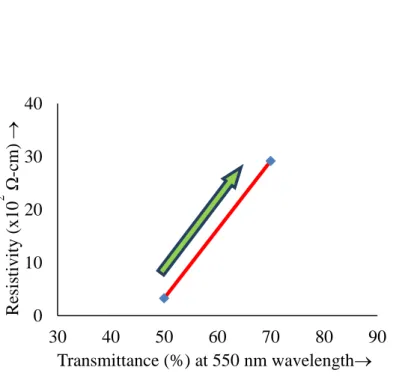
Furthermore, for the inverted planar architecture of perovskite solar cells, we need transparent p-type transport layers. The challenges of using metal oxide as p-type TCO layers are: few p-type TCOs are known, difficulties in the doping of p-type oxides materials, oxygen vacancy kills holes, hole mobility is lower than that of electrons and so on [42]–[44]. As revealed in Fig.1.6, the resistivity increases with an increased transmittance of sputtered NiOx thin films deposited on glass substrates. So, while using
TCO materials, we need to compromise with transparency and conductivity, which is a big dilemma. In the present research work, we will use both p- and n-type TCO to improve the performance of perovskite solar cells.
Fig. 1.6. Resistivity vs. transmittance of sputtered NiOx thin films on glass substrates.
R esis ti vit y (x1 0 2 Ω -c m) Transmittance (%) at 550 nm wavelength
1.3 Motivation
Wide band gap oxides and transparent conductive oxides are attractive candidates as photoactive components, hole/electron transport layers and window materials for solar cells. The purpose of this study is to use environmentally friendly, inexpensive, abundant and durable metal oxides in solar cells for improved performance. Exploring simple fabrication method and improving the properties of materials can be a good approach to reduce the cost of efficient solar cell. The main goal of this research work is to investigate the reasons behind the poor durability of the perovskite solar cell and apply new strategies to enhance the durability. This project addresses the development of materials’ properties and fabrication methods of oxide thin films, and solves the current research challenges using oxide materials to achieve efficient and durable perovskite solar cell so that this emerging technology can move from the laboratory bench to an industrial scale.
1.4 Thesis outline
The design of this dissertation is described in this section. In the first chapter (Chapter
1), the background, challenges and motivation of the current research work are
introduced. The prospect and application of metal oxide photoactive materials in solar cells will be discussed in Chapter 2. In Chapter 3, the prospect and application of metal oxide as carrier transport layers in PVSC will be described. The role of transparent conductive oxide layers (TCO) in PVSC will be described in Chapter 4. Finally, in Chapter 5, summary and impact of the current research work will be discussed and future research direction will be presented.
References
[1] M. B. Islam, M. M. Rahman, M. K. R. Khan, M. A. Halim, M. A. Sattar, D. K. Saha, and M. A. Hakim, “Spray pyrolized Ag-N co-doped p-type ZnO thin films’ preparation and study of their structural, surface morphology and opto-electrical properties,” Thin Solid Films, vol. 534, pp. 137–143, 2013.
[2] K. W. J. Barnham, M. Mazzer, and B. Clive, “Resolving the energy crisis: nuclear or photovoltaics?,” Nat. Mater., vol. 5, no. 3, pp. 161–164, 2006.
[3] G. P. Peters, G. Marland, C. Le Quéré, T. Boden, J. G. Canadell, and M. R. Raupach, “Rapid growth in CO2 emissions after the 2008–2009 global financial crisis,” Nat. Clim. Chang., vol. 2, no. 1, pp. 2–4, 2011.
[4] J. H. Noh, S. H. Im, J. H. Heo, T. N. Mandal, and S. Il Seok, “Chemical management for colorful, efficient, and stable inorganic-organic hybrid nanostructured solar cells,” Nano Lett., vol. 13, no. 4, pp. 1764–1769, 2013. [5] A. Kojima, K. Teshima, Y. Shirai, and T. Miyasaka, “Organometal halide
perovskites as visible-light sensitizers for photovoltaic cells,” J. Am. Chem. Soc., vol. 131, no. 17, pp. 6050–6051, 2009.
[6] S. A. Kulkarni, T. Baikie, P. P. Boix, N. Yantara, N. Mathews, and S. Mhaisalkar, “Band-gap tuning of lead halide perovskites using a sequential deposition process,” J. Mater. Chem. A, vol. 2, no. 24, pp. 9221–9225, 2014.
[7] M. I. Saidaminov, A. L. Abdelhady, B. Murali, E. Alarousu, V. M. Burlakov, W. Peng, I. Dursun, L. Wang, Y. He, G. Maculan, A. Goriely, T. Wu, O. F. Mohammed, and O. M. Bakr, “High-quality bulk hybrid perovskite single crystals within minutes by inverse temperature crystallization,” Nat. Commun.,
[8] G. Xing, N. Mathews, S. S. Lim, Y. M. Lam, S. Mhaisalkar, and T. C. Sum, “Reports 10.,” vol. 6960, no. 2012, pp. 498–500, 2013.
[9] S. D. Stranks, S. D. Stranks, G. E. Eperon, G. Grancini, C. Menelaou, M. J. P. Alcocer, T. Leijtens, L. M. Herz, A. Petrozza, and H. J. Snaith, “Electron-Hole Diffusion Lengths Exceeding,” Science, vol. 342, no. 2013, pp. 341–344, 2014. [10] J. M. Ball, M. M. Lee, A. Hey, and H. J. Snaith, “Low-temperature processed
meso-superstructured to thin-film perovskite solar cells,” Energy Environ. Sci., 2013.
[11] H.-S. Kim, C.-R. Lee, J.-H. Im, K.-B. Lee, T. Moehl, A. Marchioro, S.-J. Moon, R. Humphry-Baker, J.-H. Yum, J. E. Moser, M. Grätzel, and N.-G. Park, “Lead Iodide Perovskite Sensitized All-Solid-State Submicron Thin Film Mesoscopic Solar Cell with Efficiency Exceeding 9%,” Sci. Rep., vol. 2, pp. 1–7, 2012. [12] L. Meng, J. You, T.-F. Guo, and Y. Yang, “Recent Advances in the Inverted
Planar Structure of Perovskite Solar Cells,” Acc. Chem. Res., p. acs.accounts.5b00404, 2015.
[13] M. Liu, M. B. Johnston, and H. J. Snaith, “Efficient planar heterojunction perovskite solar cells by vapour deposition,” Nature, vol. 501, no. 7467, pp. 395– 398, 2013.
[14] H. Rao, W. Sun, S. Ye, W. Yan, Y. Li, H. Peng, Z. Liu, Z. Bian, and C. Huang, “Solution-Processed CuS NPs as an Inorganic Hole-Selective Contact Material for Inverted Planar Perovskite Solar Cells,” ACS Appl. Mater. Interfaces, vol. 8, no. 12, pp. 7800–7805, 2016.
[15] Z. Zhu, Y. Bai, X. Liu, C.-C. Chueh, S. Yang, and A. K.-Y. Jen, “Enhanced Efficiency and Stability of Inverted Perovskite Solar Cells Using Highly
Crystalline SnO 2 Nanocrystals as the Robust Electron-Transporting Layer,” Adv.
Mater., pp. 6478–6484, 2016.
[16] M. A. Green, K. Emery, Y. Hishikawa, W. Warta, E. D. Dunlop, D. H. Levi, and A. W. Y. Ho-Baillie, “Solar cell efficiency tables (version 49),” Prog.
Photovoltaics Res. Appl., vol. 25, no. 1, pp. 3–13, Jan. 2017.
[17] T. Xu, L. Chen, Z. Guo, and T. Ma, “Strategic improvement of the long-term stability of perovskite materials and perovskite solar cells,” Phys. Chem. Chem.
Phys., vol. 18, no. 39, pp. 27026–27050, 2016.
[18] D. Bi, W. Tress, M. I. Dar, P. Gao, J. Luo, C. Renevier, K. Schenk, A. Abate, F. Giordano, J.-P. Correa Baena, J.-D. Decoppet, S. M. Zakeeruddin, M. K. Nazeeruddin, M. Gra tzel, and A. Hagfeldt, “Efficient luminescent solar cells based on tailored mixed-cation perovskites,” Sci. Adv., vol. 2, no. 1, pp. e1501170–e1501170, 2016.
[19] K. Miyano, N. Tripathi, M. Yanagida, and Y. Shirai, “Lead Halide Perovskite Photovoltaic as a Model p-i-n Diode,” Acc. Chem. Res., vol. 49, no. 2, pp. 303– 310, 2016.
[20] N. Tripathi, Y. Shirai, M. Yanagida, A. Karen, and K. Miyano, “Novel Surface Passivation Technique for Low-Temperature Solution-Processed Perovskite PV Cells,” ACS Appl. Mater. Interfaces, vol. 8, no. 7, pp. 4644–4650, 2016.
[21] Q. Wang, C. C. Chueh, M. Eslamian, and A. K. Y. Jen, “Modulation of PEDOT:PSS pH for efficient inverted perovskite solar cells with reduced potential loss and enhanced stability,” ACS Appl. Mater. Interfaces, vol. 8, no. 46, pp. 32068–32076, 2016.
[22] W. Chen, Y. Wu, Y. Yue, J. Liu, W. Zhang, X. Yang, H. Chen, E. Bi, I. Ashraful, M. Gratzel, and L. Han, “Efficient and stable large-area perovskite solar cells with inorganic charge extraction layers,” Science (80-. )., vol. 350, no. 6263, pp. 944–948, Nov. 2015.
[23] I. S. Kim, D. H. Cao, D. B. Buchholz, J. D. Emery, O. K. Farha, J. T. Hupp, M. G. Kanatzidis, and A. B. F. Martinson, “Liquid Water- and Heat-Resistant Hybrid Perovskite Photovoltaics via an Inverted ALD Oxide Electron Extraction Layer Design,” Nano Lett., vol. 16, no. 12, pp. 7786–7790, 2016.
[24] X. Yin, P. Chen, M. Que, Y. Xing, W. Que, C. Niu, and J. Shao, “Highly Efficient Flexible Perovskite Solar Cells Using Solution-Derived NiOx Hole Contacts,” ACS Nano, vol. 10, no. 3, pp. 3630–3636, 2016.
[25] X. Yin, M. Que, Y. Xing, and W. Que, “High efficiency hysteresis-less inverted planar heterojunction perovskite solar cells with a solution-derived NiO x hole
contact layer,” J. Mater. Chem. A, vol. 3, no. 48, pp. 24495–24503, 2015.
[26] H. Zhang, J. Cheng, F. Lin, H. He, J. Mao, K. S. Wong, A. K. Y. Jen, and W. C. H. Choy, “Pinhole-free and surface-nanostructured niox film by room-Temperature solution process for high-performance flexible perovskite solar cells with good stability and reproducibility,” ACS Nano, vol. 10, no. 1, pp. 1503– 1511, 2016.
[27] U. Kwon, B.-G. Kim, D. C. Nguyen, J.-H. Park, N. Y. Ha, S.-J. Kim, S. H. Ko, S. Lee, D. Lee, and H. J. Park, “Solution-Processible Crystalline NiO Nanoparticles for High-Performance Planar Perovskite Photovoltaic Cells,” Sci. Rep., vol. 6, no. 1, p. 30759, 2016.
[28] J. H. Kim, P. W. Liang, S. T. Williams, N. Cho, C. C. Chueh, M. S. Glaz, D. S. Ginger, and A. K. Y. Jen, “High-performance and environmentally stable planar heterojunction perovskite solar cells based on a solution-processed copper-doped nickel oxide hole-transporting layer,” Adv. Mater., vol. 27, no. 4, pp. 695–701, 2015.
[29] J. You, L. Meng, T.-B. Song, T.-F. Guo, Y. (Michael) Yang, W.-H. Chang, Z. Hong, H. Chen, H. Zhou, Q. Chen, Y. Liu, N. De Marco, and Y. Yang, “Improved air stability of perovskite solar cells via solution-processed metal oxide transport layers,” Nat. Nanotechnol., vol. 11, no. 1, pp. 75–81, 2015. [30] A. B. Huang, J. T. Zhu, J. Y. Zheng, Y. Yu, Y. Liu, S. W. Yang, S. H. Bao, L.
Lei, and P. Jin, “Achieving high-performance planar perovskite solar cells with co-sputtered Co-doping NiO x hole transport layers by efficient extraction and
enhanced mobility,” J. Mater. Chem. C, vol. 4, no. 46, pp. 10839–10846, 2016. [31] J. H. Park, J. Seo, S. Park, S. S. Shin, Y. C. Kim, N. J. Jeon, H. W. Shin, T. K.
Ahn, J. H. Noh, S. C. Yoon, C. S. Hwang, and S. Il Seok, “Efficient CH<inf>3</inf>NH<inf>3</inf>PbI<inf>3</inf> Perovskite Solar Cells Employing Nanostructured p-Type NiO Electrode Formed by a Pulsed Laser Deposition,” Adv. Mater., vol. 27, no. 27, pp. 4013–4019, 2015.
[32] X. Yin, J. Liu, J. Ma, C. Zhang, P. Chen, M. Que, Y. Yang, W. Que, C. Niu, and J. Shao, “Solvothermal derived crystalline NiOx nanoparticles for high performance perovskite solar cells,” J. Power Sources, vol. 329, pp. 398–405, 2016.
[33] J. Y. Jeng, K. C. Chen, T. Y. Chiang, P. Y. Lin, T. Da Tsai, Y. C. Chang, T. F. Guo, P. Chen, T. C. Wen, and Y. J. Hsu, “Nickel oxide electrode interlayer in
CH3NH3PbI 3 perovskite/PCBM planar-heterojunction hybrid solar cells,” Adv.
Mater., vol. 26, no. 24, pp. 4107–4113, 2014.
[34] F. K. Aldibaja, L. Badia, E. Mas-Marzá, R. S. Sánchez, E. M. Barea, and I. Mora-Sero, “Effect of different lead precursors on perovskite solar cell performance and stability,” J. Mater. Chem. A, vol. 3, no. 17, pp. 9194–9200, 2015.
[35] D. Wang, M. Wright, N. K. Elumalai, and A. Uddin, “Stability of perovskite solar cells,” Sol. Energy Mater. Sol. Cells, vol. 147, pp. 255–275, 2016.
[36] H. Tsai, W. Nie, J.-C. Blancon, C. C. Stoumpos, R. Asadpour, B. Harutyunyan, A. J. Neukirch, R. Verduzco, J. J. Crochet, S. Tretiak, L. Pedesseau, J. Even, M. A. Alam, G. Gupta, J. Lou, P. M. Ajayan, M. J. Bedzyk, M. G. Kanatzidis, and A. D. Mohite, “High-efficiency two-dimensional Ruddlesden–Popper perovskite solar cells,” Nature, vol. 536, no. 7616, pp. 312–316, 2016.
[37] A. Mei, X. Li, L. Liu, Z. Ku, T. Liu, Y. Rong, M. Xu, M. Hu, J. Chen, Y. Yang, M. Gratzel, and H. Han, “A hole-conductor-free, fully printable mesoscopic perovskite solar cell with high stability,” Science (80-. )., vol. 345, no. 6194, pp. 295–298, 2014.
[38] M. Saliba, T. Matsui, J.-Y. Seo, K. Domanski, J.-P. Correa-Baena, M. K. Nazeeruddin, S. M. Zakeeruddin, W. Tress, A. Abate, A. Hagfeldt, and M. Grätzel, “Cesium-containing triple cation perovskite solar cells: improved stability, reproducibility and high efficiency,” Energy Environ. Sci., vol. 9, no. 6, pp. 1989–1997, 2016.
[39] K. A. Bush, C. D. Bailie, Y. Chen, A. R. Bowring, W. Wang, W. Ma, T. Leijtens, F. Moghadam, and M. D. McGehee, “Thermal and Environmental Stability of
Semi-Transparent Perovskite Solar Cells for Tandems Enabled by a Solution-Processed Nanoparticle Buffer Layer and Sputtered ITO Electrode,” Adv. Mater., vol. 28, no. 20, pp. 3937–3943, May 2016.
[40] W. Chen, Y. Wu, Y. Yue, J. Liu, W. Zhang, X. Yang, H. Chen, E. Bi, I. Ashraful, M. Gratzel, and L. Han, “Efficient and stable large-area perovskite solar cells with inorganic charge extraction layers,” Science (80-. )., vol. 350, no. 6263, pp. 944–948, 2015.
[41] J. Burschka, N. Pellet, S.-J. Moon, R. Humphry-Baker, P. Gao, M. K. Nazeeruddin, and M. Grätzel, “Sequential deposition as a route to high-performance perovskite-sensitized solar cells,” Nature, vol. 499, no. 7458, pp. 316–319, Jul. 2013.
[42] A. Miglio, D. Waroquiers, G. Rignanese, and X. Gonze, “High-Throughput Computational Analysis,” 2014.
[43] J. B. Varley, A. Miglio, V. A. Ha, M. J. Van Setten, G. M. Rignanese, and G. Hautier, “High-Throughput Design of Non-oxide p-Type Transparent Conducting Materials: Data Mining, Search Strategy, and Identification of Boron Phosphide,” Chem. Mater., vol. 29, no. 6, pp. 2568–2573, 2017.
[44] G. Hautier, A. Miglio, G. Ceder, G.-M. Rignanese, and X. Gonze, “Low Hole Effective Mass p-type Transparent Conducting Oxides: Identification and Design Principles,” Nat. Commun., vol. 4, pp. 1–7, 2013.
Chapter 2
Metal oxide photoactive materials
2.1 Introduction
Cuprous oxide (Cu2O) has long been attracting much interest in solar cell applications,
as the low cost and non-toxic p-type semiconductor photoactive material with a direct energy gap of 2.1 eV [1]. Obtaining n-type material from Cu2O is very difficult because
the techniques of n-type doping of Cu2O do not exist. So that homojunction cell of
Cu2O could not be fabricated so far. The present research direction is to fabricate the
Schottky barrier and heterojunction solar cells of Cu2O [2]. T. Minami et al. reported a
conversion efficiency of 5.38% in a p–n junction Cu2O thin film solar cell. However,
this is low in comparison to the theoretical energy conversion efficiency of a Cu2O solar
cell which is as high as 20% [3]. Fabricating efficient thin film solar cell based on Cu2O
faces the problems to stabilize the surface of the Cu2O sheets and enhance their quality.
Moreover, we have to achieve a lower resistivity and higher carrier concentration. A number of methods can be used to produce Cu2O, e.g. pulsed laser deposition,
sputtering, chemical vapor deposition, atomic layer deposition, spray pyrolysis, electrochemical deposition, anodic oxidation and thermal oxidation of highly pure Cu metal [4]. Among them thermal oxidation is a very promising process at low cost. It can be easily carried out at ambient atmosphere for the sheet of large areas, which has a big advantage over vacuum deposition techniques that require expensive deposition systems. This research work aims to find out an easy and efficient way to fabricate high quality Cu2O sheets by oxidizing Cu sheets.
2.2 Experimental details
Industrial grade copper sheets of 0.2 mm thickness and 99.99% purity were cut into the standard sizes of 25 mm×25 mm by a computer controlled micro-cutter. Preparation of Cu2O sheets was done by oxidizing these Cu sheets in a tube furnace. At first the
surface of Cu sheets was cleaned in diluted nitric acid followed by repeatedly rinsing in deionized water and after that dried/wiped with tissue paper. The purpose of this step was to remove any dust and pre-oxide layer on the surface of Cu sheets. After the surface preparation, the Cu sheets were annealed in an N2 gas atmosphere up to the
oxidation temperature in the tube furnace. Then the oxidation was carried out in the air at the desired temperature for one hour in the same tube furnace. A range of oxidation temperature was from 950 ºC to 1060 ºC. After completing the oxidation, the temperature was lowered to 500 ºC in N2 gas atmosphere. Finally, the oxidized sheets
were brought out from the tube furnace to the air as revealed in Fig. 2.1.
The oxidized copper sheets were characterized by the techniques of Hall measurements, ray diffraction (XRD), Scanning Electron Microscope (SEM), Energy Dispersive X-ray Spectroscopy (EDX), X-X-ray photoelectron Spectroscopy (XPS), Auger Electron Spectroscopy (AES), etc.
2.3 Results and discussion
Fabricated sheets were characterized by different techniques to find out the optimum condition for the preparation of good quality Cu2O sheets.
20 25 30 35 40 45 50 55 60 65 70 75 80 X-ray inte nsity (c ps) 2 (degrees) 950 oC CuO (111) Cu 2 O (110) Cu 2 O (211) Cu 2 O (311) Cu 2 O (220) Cu 2 O (311) 1010 oC Cu 2 O (220)
Fig. 2.2. XRD patterns of the sheet oxidized at 950 ºC and 1010 ºC.
2.3.1 Structure and morphology
X-ray diffraction (XRD) patterns of oxidized sheets are shown in Fig. 2.2: after oxidization at 950 ºC and 1010 ºC for 60 minutes. From these patterns we can see that the sheet oxidized at 950 ºC contains both Cu2O and CuO (at 38.48º of 2), while the
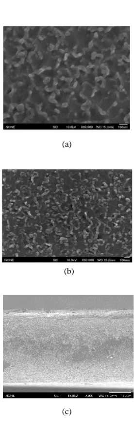
sheet oxidized at 1010 ºC consists of a single phase of Cu2O. The SEM images of the
latter sample are shown in Fig. 2.3. From the figures we can see the uneven surface morphology with nano-belt or leaf like structure.
(a)
(b)
(c)
Fig. 2.3. SEM images of the sheet oxidized at 1010 ºC at the magnification of
2.3.2 Electrical properties
The results of Hall measurements are summarized in Table 2.1. From Hall measurements, we found that the oxidized copper sheets are p-type semiconductors, since the carriers are holes in this material. We have achieved low resistivities on the order of 102 -104 Ωcm and hole concentrations on the order of 1013-1014 cm−3 with the actual values being 2.30 X 10¹³ to 7.20 X 10¹⁴. The copper sheet oxidized at 1030 ºC
shows the maximum carrier concentration and the copper sheet oxidized at 1060 ºC shows the minimum resistivity.
Table 2.1. Hall measurements data.
Oxidation Temperature (C) Resistivity X 1002 (Ωcm) Mobility (cm2/Vs) Carrier Concentration X 1013 (cm−3) 1010 154 18.2 2.30 1020 100 23.4 3.96 1030 5.14 45.5 72.0 1040 3.71 52.1 49.7 1050 4.31 51.7 33.2 1060 2.34 61.7 65.2
2.3.3 Compositional analysis
The EDX spectra of the quantitative composition of the sheet oxidized at 1010 ºC is shown in Fig. 2.4. The sheet contains 60.32 at% copper and 39.68 at% oxygen as we can see from the Table 2.2. This suggests that the samples are not fully Cu2O. Atomic
composition of Cu2O should be 66.66% Cu; 33.33% O and atomic composition of CuO
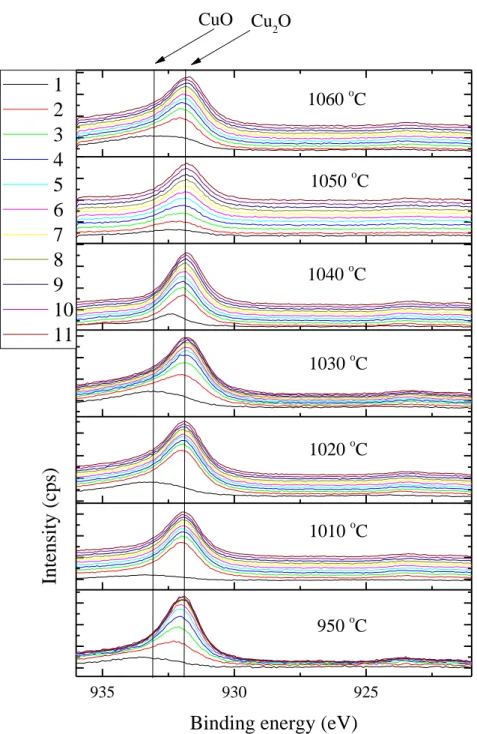
should be 50% Cu; 50% O. This can be explained by the XPS and AES spectra. Fig. 2.5 shows the wide area XPS spectra of oxidized sheets. Here, the spectrum shows the oxidized state of the copper sheet, which corresponds well with Cu 2p1/2, 2p3/2, 3s, 3p;
Cu LMM; O KLL; O 1s; and C 1s. More details can be obtained from the narrow area XPS spectra in Fig. 2.6. The depth profiling was performed for 30 minutes at the etching rate of 1 nm/minute with the intervals of 30 seconds. Fig. 2.6 shows that the surface layer contains CuO. Depth profiling illustrates that after removal of the outermost surface, the sample contains Cu2O. So, before depositing another n-type layer
on the oxidized copper sheet, we have to remove the surface layer by etching. Another important observation is that the peak position of Cu2O of the sheet oxidized at 950 ºC
is somewhat shifted to the left position. This may be due to the fact that trace amount of CuO phase exists. With increasing oxidation temperature the peak position of Cu2O
Fig. 2.4. EDAX spectra of the sheet oxidized at 1010 ºC.
Table 2.2. EDX data of the sheet oxidized at 1010 ºC.
Elements Wt % At % O 14.21 39.68 Cu 85.79 60.32 Total 100.00 100.00 1.00 2.00 3.00 4.00 5.00 6.00 7.00 8.00 9.00 Energy (keV) Int ens it y (c oun ts)
1000 800 600 400 200 0 Cu 3d O KLL Cu LMM O 1s Cu 2p 1/2 Cu 2p 3/2 C 1s Cu 3s Intensi ty (c ps)
Binding energy (eV)
Cu 3p
Fig. 2.5. Wide XPS spectra of the sheet oxidized at 1030 ºC.
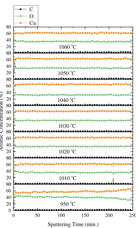
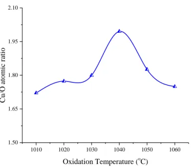
AES depth profiling curves of the fabricated sheets at various temperatures are shown in Fig. 2.7. From Fig. 2.7, we can see that the sheet oxidized at 950 ºC does not maintain the atomic composition of Cu2O i.e. 66.66% Cu; 33.33% O. On the other hand
with increasing oxidation temperature the sheets maintain the atomic composition of Cu2O in the depth profiling at the etching rate of 34 nm/minute. Again, the sheets
oxidized at 1050 and 1060 ºC show higher oxygen content than the atomic composition of Cu2O, while those oxidized at 1040 ºC show Cu:O 2:1 (Fig. 2.8). From electrical
characterization we can observe that the copper sheet oxidized at 1030 ºC and 1060 ºC shows the maximum carrier concentration and minimum resistivity respectively. However, the carrier concentration decreases against increasing oxidation temperature above 1030 ºC, but increases again at 1060 ºC. So, at or above 1030 ºC like 1040 ºC, 1050 ºC or 1060 ºC is the optimum oxidation temperature.
935 930 925 CuO Cu2O 1060 oC 1050 oC 1040 oC 1030 oC 1020 oC 1010 oC
Binding energy (eV)
950 oC
Intensity (cps)
1
2
3
4
5
6
7
8
9
10
11
Fig. 2.6. XPS depth profiling curves of the sheet oxidized at 950 ºC, 1010 ºC, 1020 ºC,
1030 ºC, 1040 ºC, 1050 ºC and 1060 ºC. Total time for etching by Ar ions are (1) 0 sec (surface), (2) 30 sec, (3) 60 sec, (4) 90 sec, (5) 120 sec, (6) 150 sec, (7) 180 sec, (8) 210 sec, (9) 240 sec, (10) 270 sec and (11) 300 sec.
0 50 100 150 200 250 0 20 40 60 800 20 40 60 800 20 40 60 800 20 40 60 800 20 40 60 800 20 40 60 800 20 40 60 80 1060 oC 1050 oC 1040 oC 1030 oC 1020 oC 1010 oC
Sputtering Time (min.) C O Cu 950 oC Atomic Conc entration (%)
Fig. 2.7. AES depth profiling curves of the sheet oxidized at 950 ºC, 1010 ºC, 1020 ºC,
1010 1020 1030 1040 1050 1060 1.50 1.65 1.80 1.95 2.10 Cu/O atom ic r ati o Oxidation Temperature (oC)
Fig. 2.8. Variation of Cu/O atomic ratio with oxidation temperature from AES
(sputtering time: 1 x 10⁴ to 1.5 x 10⁴ sec).
Table 2.3. Cu sheet oxidation conditions.
Oxidation Temperature
(C) Oxidation Atmosphere Results
1030 Oxygen Melted and reacted with boat
1060 Air almost Cu2O
1050 Air almost Cu2O
1040 Air almost Cu2O
1030 Air almost Cu2O
1020 Air almost Cu2O
1010 Air CuO & Cu2O
1000 Air CuO & Cu2O
We have also tried to oxidize the Cu sheet in the oxygen environment at 1030 ºC, but the samples were melted and reacted with the glass boat in the tube furnace. The result of oxidation in different conditions is summarized in Table 2.3. We reported this results in the International Journal of Computer Science and Electronics Engineering (IJCSEE) [5].
2.4 Summary and conclusions
Cu2O sheets were successfully fabricated by oxidizing Cu sheets in air environment.
We also tried to prepare Cu2O sheets in an oxygen environment but the Cu sheets were
melted and reacted with the glass boat. So, according to our investigation an oxidizing treatment at or above 1030 ºC in air environment like 1040 ºC, 1050 ºC or 1060 ºC is appropriate to oxidize the copper sheet for fabricating cuprous oxide. However, prepared cuprous oxide sheets, as a photoactive material, were too brittle to fabricate solar cell device.
References
[1] T. Minami, T. Miyata, and Y. Nishi, “Efficiency improvement of Cu2O-based heterojunction solar cells fabricated using thermally oxidized copper sheets,”
Thin Solid Films, vol. 559, pp. 105–111, 2014.
[2] A. . Musa, T. Akomolafe, and M. . Carter, “Production of cuprous oxide, a solar cell material, by thermal oxidation and a study of its physical and electrical properties,” Sol. Energy Mater. Sol. Cells, vol. 51, no. 3–4, pp. 305–316, 1998. [3] T. Minami, T. Miyata, and Y. Nishi, “Cu2O-based heterojunction solar cells with
an Al-doped ZnO/oxide semiconductor/thermally oxidized Cu2O sheet structure,”
Sol. Energy, vol. 105, pp. 206–217, 2014.
[4] M. Pavan, S. Rühle, A. Ginsburg, D. A. Keller, H. N. Barad, P. M. Sberna, D. Nunes, R. Martins, A. Y. Anderson, A. Zaban, and E. Fortunato, “TiO2/Cu2O all-oxide heterojunction solar cells produced by spray pyrolysis,” Sol. Energy
Mater. Sol. Cells, vol. 132, pp. 549–556, 2015.
[5] M. B. Islam, Y. Nabetani, and E. Torikai, “Facile Preparation of High Quality p-Type Cu 2 O for Thin Film Solar Cells,” vol. 4, no. 1, pp. 2–7, 2016.
Chapter 3
Metal oxide transport layers
3.1 Introduction
After the invention of organic-inorganic hybrid perovskite solar cell with 3.81% power conversion efficiency by Kojima et. al. [1], it has attracted much attention because of its low cost and easy fabrication. Within a very short period of time, PVSCs have achieved a rapid development and the PCE exceeded 20%, comparable to those of the conventional silicon solar cells [2], [3]. There have also been a growing interest in the development of low-temperature processed PVSCs with inverted device structures because of the lower fabrication cost and new solar cell applications with its light weight and flexibility. However, it is still a great challenge to fabricate long-lifetime PVSCs using low-temperature processes for successful commercialization. Although the impressive high efficiency of PVSCs stands up to those of other existing PV technologies with 20% efficiency, the rapid degradation phenomena broadly observed for PVSCs overshadow the future of this PV technology [4]. The literature concerning the real performance of the PVSCs in long-term operations is still limited, and many studies on the perovskite stabilities focus on the stored life-time (shelf-life)[5], [6]. As far as we know, there have been only a few reports on the stability of the operating conditions of PVSCs under light [7]–[12]. The purpose of this study is to examine the effect of an interface layer on the long-term operation of low-temperature processed PVSCs under real working conditions, with maximum power point tracking (MPPT) under 1SUN (AM1.5G) illumination (no UV light filtering).
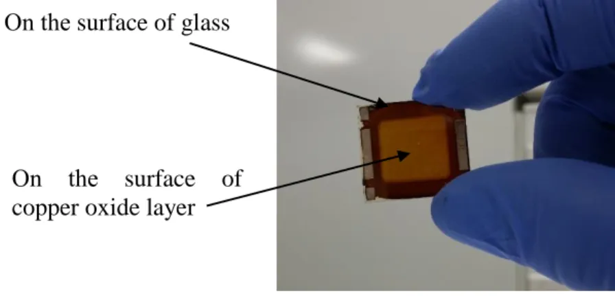
One of the possible reasons for the instability of the PVSCs is due to the instability and/or adverse effect of the organic hole transport layers [13]–[16], and we set out to develop an ideal HTL which have a suitable energy level with perovskite, high optical transparency in the visible range, and high stability and supports the fabrication of thick and high quality perovskite films. Due to the direct bandgap of 2.17 eV and low electron affinity of 3.2 eV, copper oxide could be a good HTL for PVSCs [17]. However, we found that perovskite layer is not stable at the top of the sputter deposited copper oxide layer. As shown in Fig.3.1, perovskite layer turns to yellow within 30 minutes of preparation. It might be due to the reverse reaction of perovskite formation on the surface of copper oxide.
Perovskite formation, PbI2 + CH3NH3I CH3NH3PbI3-xClx
On the surface of copper oxide, CH3NH3PbI3-xClx PbI2 + CH3NH3I
Fig. 3.1. Dissociation of perovskite layer on the surface of the copper oxide layer.
On the other hand, owing to its large bandgap (3.6 eV), deep valance band edge (5.4 eV), ease of controlling composition, and low cost with superior thermal and chemical On the surface of glass
On the surface of copper oxide layer
have been used for the fabrication of inverted and other type of PVSCs, and the stability issue often became a focus in studies concerning them [7], [14], [16], [18]–[37]. In this study, we demonstrate the inverted planar PVSCs on the basis of the sputter-deposited polycrystalline NiOx hole transport material. We prepared compact and homogeneous
NiOx films on ITO coated glass by rf magnetron sputtering, allowing us to control the
oxygen composition and thickness, with high reproducibility [20]. We revealed in detail the effect of NiOx composition and thickness (from 20 to 250 nm) on the device
performance and showed that fine-tuning of the composition (Ni3+/Ni2+ ratio) and thickness resulted in the high performance PVSCs with over 15% efficiency and unprecedented stability for low temperature-processed MAPbI3-xClx devices. We also
compared the stability of the NiOx-based devices and the PEDOT:PSS-based devices
under the continuous illumination from a class AAA solar simulator at MPPT condition. We clearly demonstrated that the illumination-induced degradation significantly depends on of the nature of the HTL in the inverted PVSCs. The sputtered NiOx HTL
can be a good candidate to solve stability problems in the low-temperature-processed lead halide PVSCs.
3.2 Experimental details
For the preparation of PVSCs, at first the NiOx thin films were prepared using an rf
magnetron sputtering system and after that the remaining steps were performed in a nitrogen filled glovebox. Finally, the rf magnetron sputtering was used to metal contact (silver) deposition. Details of experimental methods are described below.
3.2.1 NiOx Film deposition
The NiOx thin films were prepared on the commercially available precleaned and
prepatterned indium tin oxide (ITO)-coated glass substrates using an rf magnetron sputtering system (SVC-700 RFIINA, Sanyu Electron, Japan). Substrates for devices and glasses for characterizing the structural, optical, electrical and compositional properties were deposited in the same batch for side-by-side comparison. All the substrates were treated with ultraviolet-ozone for 20 min and immediately loaded in the deposition chamber. Before deposition, the chamber was evacuated until the pressure inside it becomes < 2×10⁻³ Pa; then, pure argon gas was introduced at the rate of 20 sccm. Sputter deposition was carried out in an argon gas pressure of 0.5-6.5 Pa and a radio frequency (rf) power supply of 50 W. The thickness of the NiOx films for pressure
3.5 Pa was about 60 – 70 nm and that for 5.0 Pa was about 40 nm. The thicknesses of the NiOx films were controlled by regulating the deposition time from 20 min to 2 h.
Sputter deposition was further carried out in an argon gas pressure of 3.5 Pa and a radio frequency (rf) power supply of 50 W (2 h), 100 W (1 h) and 200 W (20 min), thickness of NiOx films were 704 nm. Commercially available sintered 99.9% pure NiO was
used as the target (Kojundo Chemical Laboratory co. Ltd., Japan). All procedures were carried out in room temperature (no intentional heating).
3.2.2 Materials and characterizations
All chemicals were purchased from commercial suppliers and used as received, unless stated otherwise. Perovskite precursor solutions were prepared by dissolving PbI2
(Kanto-chemical, 98% purity) in anhydrous N, N-dimethylformamide (DMF) (400 mg mL−1), and methylammonium iodide (MAI) and methylammonium chloride (MACl)
(Wako Chemicals, battery grade) in ethanol (50 mg mL−1, 19:1 ratio). PC61BM (Sigma
Aldrich, 99% purity) solution (2 wt. %) dissolved in anhydrous chlorobenzene was used for coating the electron transport layer. All solutions were filtered through 0.45 μm syringe filters to avoid the risk of particle formation. Aluminum doped zinc oxide (AZO) nanoparticle ink (Nanograde N-21X) was used to prepare the AZO layer. The X-ray diffraction (XRD) patterns were collected using an X-X-ray diffractometer (Rigaku SmartLab, Japan) (Cu Kα radiation, λ= 1.54050 A). Top-surface and cross-sectional images were taken using a high-resolution scanning electron microscope (Hitachi, S-4800) at a 5 kV accelerating voltage carefully to avoid damage to the samples. X-ray photoelectron spectroscopy (XPS) (ULVAC-PHI, VersaProbe II, Japan) was used to analyze the elemental composition of the NiOx films. The UV-vis absorption spectra
were recorded on a UV-vis NIR spectrometer (7200, Jasco). The resistivity of the films was measured by a linear four probe method. The current density−voltage (J−V) characteristics (FF, Rs, and Rsh) were analyzed by a commercial software
(SYSTEMHOUSE SUNRISE corp.) and the incident monochromatic IPCE spectra and external quantum efficiency (EQE) were measured using a spectrometer (SM-250IQE, Bunkokeiki, Japan). For stability testing, the encapsulated devices were evaluated under 1 SUN illumination (AM1.5G, no UV-light filtering) and maximum power point tracking (MPPT) condition using solar simulator system equipped with temperature controlled oven (BIR-50, Bunkokeiki, Japan). A thermocouple was placed near the sample surface to monitor the testing condition. A histogram of 32 cells with NiOx HTL
(703 nm) prepared at 3.5 Pa were deduced from the devices, with an area of 0.19 cm2
3.2.3 Device fabrication
A thin layer (~30 nm) of PEDOT:PSS (Clevios, Al4083) was formed by spin coating at 3000 rpm and subsequently dried at 120 °C for 15 min on a hot plate in ambient air. Sputter deposited NiOx and PEDOT:PSS substrates were transferred to a nitrogen filled
glovebox (<1.0 ppm of O2 and H2O), inside which the remaining steps were performed.
A PbI2 film was spin-coated at 3000 rpm for 90 s and then the mixture of MAI and
MACl was spun onto the PbI2 layer at 4000 rpm for 90 s for Cl-mediated interdiffusion
[38]. Then to promote the crystallization, those as grown CH3NH3PbI3-xClx perovskite
films were placed inside a Petri dish with MACl powders on hot plate at 100 ℃ for MACl treatment [39]. A PC61BM layer was spun onto the perovskite layer at 700 rpm
for 60 s, followed by coating with an AZO layer at 3000 rpm for 30 s. The samples were then transferred to the rf magnetron sputtering chamber outside the glovebox for metal contact (silver) deposition. Ag (150 nm) was sputtered at an Ar pressure of 0.15 Pa. The devices were sealed by encapsulation glasses and UV-curable resins (UV RESIN XNR5516Z, Nagase ChemteX, Japan) before measurement under ambient conditions and the stability test.
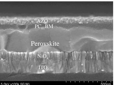
Fig. 3.2. Device structure (a) consisting of ITO coated glass/NiOx/perovskite
(CH3NH3PbI3-xClx )/PC61BM/AZO/Ag and (b) corresponding energy band diagram.
(a)
ITO coated Glass NiOx
Perovskite
PC61BM ITO AZO AgSun Light
(b)
-5.4 eV Ener gy Level (eV ) -4.8 eV -1.8 eV -5.4 eV -3.9 eV -5.9 eV -4.2 eV ITO NiOx Perovskite PC61BM AZO -5.7 eV -4.6 eV Ag e hFig. 3.3. Cross-sectional SEM image of the device.
3.3 Results and discussion
The device structure of our perovskite solar cell is shown in Fig. 3.2 (a). This inverted structure consists of ITO coated glass/NiOx/perovskite (CH3NH3PbI
3-xClx)/PC61BM/aluminum-doped zinc oxide (AZO)/Ag, where the NiOx is the hole
transport layer (or electron blocking layer) and PC61BM/AZO is the electron transport
layer. The corresponding band diagram and energy levels are shown in Fig. 3.2 (b). The scanning electron microscopy (SEM) cross-section of the device is illustrated in Fig. 3.3. Sealing glass was used to encapsulate the device, to protect it from moisture and oxygen.
3.3.1 Properties of NiOx thin films
NiOx films were fabricated at different Ar pressures of the deposition chamber; the
optical and electrical properties of the resulting NiOx films depend on the deposition
conditions, and it is found that at lower pressure, because of Ni vacancy/excess oxygen
ITO NiOx
Perovskite
PC61BM AZO(c)
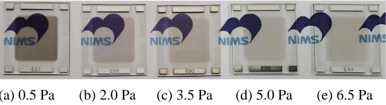
Fig. 3.4. Photographs of fabricated NiOx films at different Ar pressure of (a) 0.5, (b) 2.0,
(c) 3.5, (d) 5.0 and (e) 6.5 Pa.
This observation parallels to that of the previous study with compact NiOx
electron-blocking layers prepared by sputtering [21]. The oxygen content of the black form was slightly greater than that of its green counterpart [40]. The defect of NiO films is due to the interstitial oxygen or Ni2+ vacancy that occurs as a result of the creation of Ni3+ ions.
For each Ni2+ vacancy (Niv), two Ni2+ ions must be converted to Ni3+ to preserve overall
charge neutrality in the crystal. That ensures excess oxygen comparing to the number of nickel ions in the crystal. Then finally the creation of defects in NiOx crystals can be
expressed with the following equation,
2NiO 2Ni3+ + Niv + 2O
2-Now if an electron moves from a Ni2+ site to a Ni3+ site, it is as like the movement of a hole in the opposite direction through the Ni2+ sites. These holes contribute to the electrical conductivity of undoped NiOx crystals. Therefore NiOx with excess oxygen is
a p-type semiconductor [41].
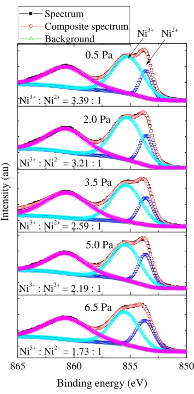
To analyze the Ni3+/ Ni2+ ratio of the sputtered NiOx thin films, they were characterized
by X-ray photoelectron spectroscopy (XPS). As shown in Fig. 3.5, the peak at 860.8 eV
(e) 6.5 Pa
(a) 0.5 Pa
(b) 2.0 Pa
(c) 3.5 Pa
(d) 5.0 Pa
is due to the shake up process of the NiO structure, the peak at 853.8 eV indicates Ni2+ ion and the peak at 855.5 eV indicates Ni3+ ion [24]. The composition of Ni2+ and Ni3+
in the crystals were determined by calculating the integral area of the fitting curve of the XPS spectra, and the Ni3+/ Ni2+ ratio of NiOx films is shown in Fig. 3.6. It is evident
from the figure that the Ni3+/ Ni2+ ratio decreased with increasing pressure.
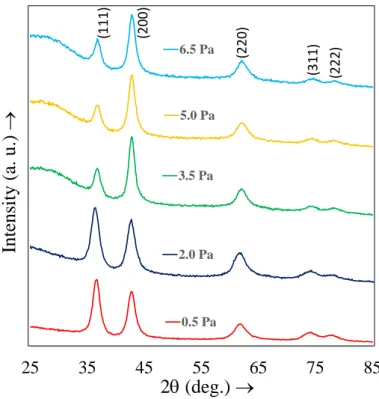
The films prepared by sputtering methods are polycrystalline in nature and have cubic structure, as shown in Fig. 3.7. At lower pressure, the (111) peak is dominating, and with increasing pressure (200) peak becomes dominating. Broader XRD peaks indicate small crystal size of the fabricated films. Furthermore, we studied the surface morphology of NiOx films by SEM, as shown in Fig. 3.8. The SEM images demonstrate
the small grains of NiOx films, and the grain size is dependent on the thickness of the
films. At a lower thickness (20 nm), the grain size is quite small, however, with increasing thickness (up to 250 nm) the grain size gradually increases.
865
860
855
850
Spectrum
Composite spectrum
Background
Binding energy (eV)
6.5 Pa
5.0 Pa
In
tensi
ty
(au)
3.5 Pa
2.0 Pa
Ni
3+Ni
2+Ni
3+: Ni
2+= 1.73 : 1
Ni
3+: Ni
2+= 2.19 : 1
Ni
3+: Ni
2+= 2.59 : 1
Ni
3+: Ni
2+= 3.21 : 1
0.5 Pa
Ni
3+: Ni
2+= 3.39 : 1
Fig. 3.5. XPS spectra representing the Ni 2p3/2 peak with deconvolution of Ni3+ and
Fig. 3.6. Composition of the NiOx films at different Ar pressure.
Fig. 3.7. X-ray Diffraction (XRD) patterns of the NiOx films at different Ar pressure.
Ar Pressure (Pa) Ni 3+ /Ni 2+ ra ti o 1 1.5 2 2.5 3 3.5 4 0 1 2 3 4 5 6 7 6.5 Pa 25 35 45 55 65 75 85 0.5 Pa 2.0 Pa Inte nsit y (a . u .) 2 (deg.) 3.5 Pa 5.0 Pa (111) (200) (2 20) (3 1 1 ) (222)
(a) (b)
(c) (d)
(e) (f)
Fig. 3.8. SEM images of fabricated NiOx films at 3.5 Pa for different thickness of (a) 20
nm, (b) 50 nm, (c) 70 nm, (d) 100 nm, (e) 150 nm and (f) 250 nm.
(f)
(e)
(d)
(b)
(a)
(c)
(f)
(e)
(d)
(b)
(a)
(c)
(d)
(e)
(f)
(b)
(a)
(c)
(f)
(e)
(d)
(b)
(a)
(c)
The Ar pressure in the sputtering chamber has little effect on the grain size (Fig. 3.9) and with increasing Ar pressure, grain size increases. With increasing Ar pressure in the sputtering chamber, the transmittance of the prepared films also increases as shown in
Fig. 3.10. The films prepared at 0.5 Pa have a lower transmittance of 60% at the 550 nm
wavelength of the visible range of the spectrum. While the films prepared at or above 3.5 Pa show more than 80% transmittance at 550 nm wavelength of the spectrum. It is noticeable that the difference of transmittance between the films prepared at 0.5 Pa and 3.5 Pa is very large (20%), while the effect is very little (5%) for the films prepared at 3.5 Pa to 6.5 Pa. Because of increasing Ni vacancy/excess oxygen, the films became blackish and their transmittance decreased at lower Ar pressure. Fig. 3.10 also compares the transmittance of the fabricated NiOx films at different thicknesses. It is
evident from the figure that transmittance declines with increasing thickness, as expected, and the only exception is at 150 nm thickness, where the transmittance is higher than that at the 70 nm thickness. The reason may be the large grain size, as shown in Fig. 3.8, which might reduce the light scattering by the grain boundary. The films prepared at 0.5 Pa and 2.0 Pa have resistivities of 3.28 x10² and 2.92 x10³ Ω-cm, respectively. However, the films prepared at the pressure range of 3.5-6.5 have very high resistivities, which we could not measure using our linear four-probe system. The low resistivity of the films prepared at lower pressure possibly indicated the increased Ni vacancy/excess oxygen in the crystals, which act as the hole and contribute to the electrical conductivity. This effect is quite consisted with the XPS and XRD results. The resistivity values of the (200)-orientated NiOx films are higher than those of the
(a) (b)
(c) (d)
(e)
Fig. 3.9. SEM images of fabricated NiOx films at different Ar pressure of (a) 0.5, (b) 2.0,
(c) 3.5, (d) 5.0 and (e) 6.5 Pa.
(e)
(a)
(b)
(c)
(d)
(e)
(a)
(b)
(c)
(d)
(e)
(a)
(b)
(c)
(d)
(e)
(a)
(b)
(c)
(d)
200 400 600 800 1000 1200 1400 0 20 40 60 80 1000 20 40 60 80 100 Tr ans mitt anc e (%) Wavelength (nm) Glass substrate 20 nm 50 nm 70 nm 100 nm 150 nm 250 nm Tr ans mitt anc e (%) Glass substrate 0.5 Pa 2.0 Pa 3.5 Pa 5.0 Pa 6.5 Pa
Fig. 3.10. Transmission spectra of NiOx films on glass substrate at different Ar pressure
(film thickness: 60–70 nm for 0.5–3.5 Pa and ~40 nm for 5.0–6.5 Pa) and at different thicknesses at Ar pressure of 3.5 Pa.
3.3.2 Device performances
We revealed the dependence of device performances on the Ar pressure during sputter deposition of NiOx, and the results are summarized in Table 3.1 and Fig. 3.11. It is
enhanced and beyond that pressure, it declined (Fig. 3.11 (a)). This phenomena can be explained with the optical and electrical properties of the sputtered NiOx thin films. As
shown in Fig. 3.10, at lower pressure, the NiOx thin films absorbed some part of the
incident sunlight. At higher pressure, although the transmittance is better, higher resistance of the films reduces the device performance, as seen from the increased series resistance (Rs) for 5.0 and 6.5 Pa. Therefore, we selected the devices with NiOx HTL
prepared at 3.5 Pa Ar pressure for further study of thickness-dependent device performance, and the results are summarized in Table 3.2.
Table 3.1. Performance of the devices with different Ar pressure of the deposition
chamber during sputter deposition of NiOx. Data collected from at least 12 cells for
each condition. (NiOx film thickness: 60–70 nm for 0.5–3.5 Pa and ~40 nm for 5.0–6.5
Pa). Ar Pressure (Pa) (%) Jsc (mA/cm2) Voc (V) FF Rs (Ω・cm2) Rsh (Ω・cm2) x103 0.5 11.020.46 17.670.71 0.970.01 0.630.03 5.010.58 2.070.19 2.0 12.210.58 18.700.83 0.980.01 0.630.02 5.160.47 2.350.72 3.5 14.760.39 19.860.85 1.010.02 0.680.02 5.410.62 3.250.33 5.0 13.610.61 19.790.69 0.980.01 0.660.03 8.850.83 2.300.46 6.5 12.090.57 18.880.48 0.980.01 0.650.04 8.740.92 1.230.57
0 1 2 3 4 5 6 7 6 7 8 9 10 11 12 13 14 15 16 Efficiency ( %) Pressure (Pa) (a) 400 600 800 0 20 40 60 80 1000 20 40 60 80 100 EQE (% ) Wavelength (nm) 20 nm 50 nm 70 nm 100 nm 150 nm 250 nm (b) EQE (% ) 0.5 Pa 2.0 Pa 3.5 Pa 5.0 Pa 6.5 Pa
Fig. 3.11. Device performances. (a) Ar pressure dependent PCE, (b) EQE of the devices
Table 3.2. Performance of the devices with different thickness of NiOx prepared at 3.5
Pa. Data collected from at least 12 cells for each thickness.
NiOx Thickness (nm) (%) Jsc (mA/cm2) Voc (V) FF Rs (Ω・cm2) Rsh (Ω・cm2) x103 202 8.250.41 18.470.23 0.980.01 0.460.11 21.481.31 0.860.15 502 13.430.56 19.890.65 1.000.01 0.620.02 5.070.45 1.470.38 703 14.760.39 19.860.85 1.010.02 0.680.02 5.410.62 3.250.33 1005 13.640.67 19.010.41 0.950.01 0.690.01 5.820.33 3.050.46 1505 14.120.35 18.740.64 0.930.02 0.730.01 5.350.52 2.830.63 2507 11.850.58 16.110.72 0.900.02 0.740.01 5.800.61 2.760.29
It was found that when the NiOx layer was too thin (e.g., 20 nm), the devices showed
lower PCE. The very thin film may be not sufficient to block the photogenerated electrons because of the insufficient coverage of the ITO film with the NiOx layer,
which in turn decreases the fill factor (FF) [23], [30]. In fact, the improved FF values with increasing thickness were observed possibly due to the elimination of pinholes. However, with a very thick NiOx HTL, the FF was satisfactory, but the PCE was again
low. With higher thickness, the transmittance decreased, with the small deviation at 150 nm thickness. From Fig. 3.11 (b), we can see that with higher thickness, the EQE of the devices decreased significantly at lower wavelength, which reduces the short circuit current density (Jsc). Devices with a NiOx HTL thickness of 703 nm showed best
performance (Fig. 3.12). Although the hysteresis behaviors of the perovskite solar cells are an important issue, which is frequently observed and reported in the literature [43],
our NiOx devices showed almost no hysteresis behaviors (Fig. 3.13). The devices
showed a good reproducibility, with a limited deviation of PCE, as shown in Fig. 3.14. Histograms of solar cell efficiencies were collected from 32 cells with NiOx HTL of 70
nm3 thickness prepared at 3.5 Pa Ar pressure.
0
50
100
150
200
250
8
12
16
12
16
20
0.6
0.8
1.0
1.2
0.40
0.60
0.80
Effic
ie
ncy
(%)
Thickness (nm)
Js
c (
mA/cm
-2)
Vo
c (
V)
FF
Fig. 3.13. J-V curve of the best device with NiOx HTL (3.5 Pa, 70 nm) under one sun
condition measured at forward scan (-0.05 V 1.2 V, step 0.02 V, delay time 200 ms) and reverse scan (1.2 V -0.05 V, step 0.02 V, delay time 200 ms).
Fig. 3.14. The PCE distribution histogram of devices with NiOx HTL prepared at 3.5 Pa.
0.0 0.2 0.4 0.6 0.8 1.0 1.2 -10 -5 0 5 10 15 20 25 Forward Reverse Jsc= 20.33 (mA/cm2) Voc= 1.08 (V) FF = 0.69 Rs= 5.99 (Ω・cm2) Rsh= 1.34 X 10³(Ω・cm2) η = 15.15 % Pint= 100 (mA/cm2) J (m A/cm 2) Voltage (V) Counts (%) PCE (%) 14.00 14.25 14.50 14.75 15.00 15.25 15.50 0 10 20 30 40 50 60
No significant performance degradation was observed for encapsulated devices with NiOx HTL stored at ambient temperature under dark condition for five months. The
significant improvement of the stability over previous NiOx based devices [7], [14], [16]
[18]-[37] was achieved possibly due to the synergy of the NiOx HTL, with the high
optoelectronic quality of the MACl treated perovskite layer [39]. We also observed that the PCE and open circuit voltage (Voc) gradually increase with time at ambient
temperature under dark condition. The improvement can be explained by the ion migration and chemical doping of the PCBM layer by iodide [8], [44]. On the other hand, under continuous 1 SUN illumination (no UV-light filtering) and MPPT condition at 30℃, the performance first degraded gradually and then the degradation rate decreased; and it eventually reached 87% of initial efficiency after 670 h of operation, as shown in Fig. 3.15. The PEDOT:PSS-based devices degrade rapidly, and within 400 h, they retain only 20% of the initial PCE, possibly due to the chemical nature of the PEDOT:PSS layer [13]-[16]. The lifetime of solar cells may be defined as the operation time until the output of the device has fallen below a certain level, that is, 70% of nominal efficiency for more than 40 years was expected from some commercial Si solar cells. In fact, the NiOx based devices showed surprisingly high stability and it would
0 100 200 300 400 500 600 700 0.2 0.4 0.6 0.8 1.0 1.2 0.2 0.4 0.6 0.8 1.0 1.2 0.2 0.4 0.6 0.8 1.0 1.2 0.2 0.4 0.6 0.8 1.0 1.2
Normalized PCE
Time (h)
Continuous illumination-NiOx
Dark-NiOx
Continuous illumination-PEDOT:PSS
Normalized J
sc
Normalized V
oc
Normalized FF
Fig. 3.15. Stability of the encapsulated device at 30℃ (~50%RH) under ambient in dark
condition and under MPPT condition (1 SUN) (The device was kept at MPPT condition between the periodical J-V measurements)