S T U D Y O F H I G H E F F I C I E N C Y A N D L O W I N P U T V O LTA G E P O W E R C O N V E R S I O N C I R C U I T S F O R E N E R G Y H A R V E S T I N G
A P P L I C AT I O N S z a c h a r y z e h n e r n o s k e r
PhD Dissertation
Submitted in Partial Fulfillment of the Requirements for the Degree of Doctor of Philosophy
Division of Electronics and Informatics School of Science and Technology
Gunma University 4February2014– Version1.6
Study of High Efficiency and Low Input Voltage Power Conversion Cir- cuits for Energy Harvesting Applications, PhD Dissertation, ©4 Febru- ary2014
s u p e r v i s o r: Haruo KOBAYASHI l o c at i o n:
Kiryu, Japan
What the result of these investigations will be the future will tell; but whatever they may be, and to whatever this principle may lead, I shall be sufficiently recompensed if later it will be admitted that I have contributed a
share, however small, to the advancement of science.
— Nikola TESLA
This dissertation is dedicated to my parents, Sue and Richard. I owe all my success to their unending love, encouragement and support.
A B S T R A C T
This dissertation summarizes research into power electronics for en- ergy harvesting and mobile device applications. In order to familiar- ize the reader with basic power electronics concepts, Chapter2gives a brief overview of power electronic circuits, from linear regulators to switching buck and boost regulators. These circuits are presented in a simplified form and it is hoped that anyone with a basic understand- ing of microelectronics will be able to follow the explanation. While there are manifold other power electronic circuits in use in the world, their large size and reliance on transformers make them impractical for mobile applications. To this end, Chapter 2focuses only on Buck (step–down) and Boost (step–up) regulators. Subsequent chapters delve deeper into the world of power electronics for mobile applications.
Since it is a new and developing field, Chapter 3 gives a survey of energy harvesting technology, including typical applications and examples of transducers that can be used as input sources. This intro- duction includes transducers that function from vibration (Piezoelec- tric Transducers), temperature difference (Thermoelectric Generators (TEGs)) and ambient light (Photovoltaic Transducers).
Chapter 4 gives a detailed account of power conversion circuits that have been introduced previously for energy harvesting applica- tions. This explanation includes circuits for Piezoelectric, Thermoelec- tric and Photovoltaic transducers, and explains the operation of each circuit as well as their shortcomings.
Chapter5introduces a small, low power bootstrapped boost regu- lator that can start up with an input voltage of 240 mV and achieve a maximum efficiency of 97%. The proposed circuit uses two sepa- rate control schemes for startup and steady-state operation. A fixed- frequency oscillator is used to initially start up the circuit and raise the output voltage. Once the output voltage has reached a level ade- quate to bias the internal circuitry, a constant-on-time style hysteretic control scheme is used to regulate the output voltage. This hysteretic control scheme helps increase system efficiency compared to using conventional Pulse-Width-Modulated control. While maintaining a high efficiency, the proposed circuit is implemented using only three external components: two capacitors (input and output) and an in- ductor. The effectiveness of this approach is shown through Spectre simulation results. Additionally, a test chip consisting of the startup charge pump was taped out and evaluated on the lab bench. Char- acterization shows that this subsystem functions correctly and that it will be able to power the drivers and output switches when the full chip is taped out together.
v
tions into the output impedance of a multi-phase buck converter.
Since these investigations into this area are outside the scope of en- ergy harvesting, and since the results have not yet reached a level of academic breakthrough, this discussion is placed in appendix Chap- ter A. As power requirements in portable devices increase, more at- tention is being paid to the load transient response of the power elec- tronic circuit, and how quickly the system can react to a change in load current. Measurement of the output impedance of the converter over frequency shows how the circuit will react to a load transient at any frequency, and can guarantee that the undershoot or overshoot is less than a certain maximum value. This data was collected using a Frequency Response Analyzer and the DA9210 4-phase buck con- verter provided by Dialog Semiconductor.
vi
P U B L I C AT I O N S
Some ideas and figures have appeared previously in the following publications:
j o u r na l pa p e r s
I Zachary Nosker, Yasunori Kobori, Haruo Kobayashi, Kiichi Ni- itsu, Nobukazu Takai, Takeshi Oomori, Takahiro Odaguchi, Isao Nakanishi, Kenji Nemoto, Jun-ichi Matsuda,A Small, Low Power Boost Regulator Optimized for Energy Harvesting Applications, Ana- log Integrated Circuits and Signal Processing 75(2), pp.207-216 (May2013).
II Zachary Nosker, Yasunori Kobori, Haruo Kobayashi, Kiichi Ni- itsu, Nobukazu Takai, Takeshi Oomori, Takahiro Odaguchi, Isao Nakanishi, Kenji Nemoto, Junichi Matsuda, A High Efficiency, Extended Load Range Boost Regulator Optimized for Energy Harvest- ing Applications, Key Engineering Materials, vol.534, pp.206-219 (Jan.2013).
III Jiani Ye,Zachary Nosker, Kazuyuki Wakabayashi, Takuya Yagi, Osamu Yamamoto, Nobukazu Takai, Kiichi Niitsu, Keisuke Kato, Takao Ootsuki, Isao Akiyama, Haruo Kobayashi,Architecture of High-Efficiency Digitally-Controlled Class-E Power Amplifier, Key Engineering Materials, vol.487, pp.273-284(Dec.2011).
IV Yohei Tan, Daiki Oki, Yu Liu, Yukiko Arai, Zachary Nosker, Haruo Kobayashi, Osamu Kobayashi, Tatsuji Matsuura, Zhixiang Yang, Atsuhiro Katayama, Li Quan, Ensi Li, Kiichi Niitsu, No- bukazu Takai, Self-Calibration Technique of Pipeline ADC Using Cyclic Configuration,Key Engineering Materials. vol.596, pp.181- 186(2014).
i n t e r nat i o na l c o n f e r e n c e pa p e r s
V Zachary Nosker, Yasunori Kobori, Haruo Kobayashi, Kiichi Ni- itsu, Nobukazu Takai, Tetsuji Yamaguchi, Eiji Shikata, Tsuyoshi Kaneko, Kimio UedaA Single Supply Bootsrapped Boost Regulator for Energy Harvesting Applications, The 2013 International Con- ference on Integrated Circuits, Design, and Verification (ICDV 2013), Ho Chi Minh City, Vietnam (November15–16,2013).
vii
Zachary Nosker, Shaiful N. Mohyar, Nobukazu Takai, Haruo Kobayashi, Takahiro Odaguchi, Isao Nakanishi, Kimio Ueda, Jun-ichi Matsuda, Single Inductor Dual Output Switching Con- verter using Exclusive Control Method, IEEE International Con- ference on Power Engineering, Energy and Electrical Devices, Istanbul, Turkey (13–17May2013).
VII Yasunori Kobori, Shunsuke Tanaka, Tatsunori Nagashima, Taka- hiro Sakai, Kotaro Kaneya, Shunichiro Todoroki,Zachary Nosker, Nobukazu Takai, Haruo Kobayashi, Takahiro Odaguchi, Isao Nakanishi, Kimio Ueda, Jun-Ichi Matsuda,High-Speed Response Single Inductor Multi Output DC-DC Converter with Hysteresis Control,1st Annual International Conference on Power, Energy and Electrical Engineering (PEEE2013) Singapore (26–27 Aug.
2013).
VIII Yasunori Kobori, Lin Xing, Hong Gao, Masanori Onozawa, Shu Wu, Shaiful Nizam Mohyar,Zachary Nosker, Haruo Kobayashi, Nobukazu Takai, Kiichi Niitsu, Non-Isolated Direct AC-DC Con- verter Design with BCM-PFC Circuit,International Conference on Power Engineering, Bali, Indonesia (Oct.2012).
IX Yasunori Kobori, Qiulin Zhu, Murong Li, Feng Zhao, Zachary Nosker, Shu Wu, Shaiful N. Mohyar, Masanori Onozawa, Haruo Kobayashi, Nobukazu Takai, Kiichi Niitsu, Takahiro Odaguchi, Isao Nakanishi, Kenji Nemoto, Jun-ichi Matsuda, Single Induc- tor Dual Output DC-DC Converter Design with Exclusive Control, IEEE Asia Pacific Conference on Circuits and Systems, Kaohsi- ung, Taiwan (Dec.2012).
X Hong Gao, Lin Xing, Yasunori Kobori, Zhao Feng, Haruo Koba- yashi, Shyunsuke Miwa, Atsushi Motozawa, Zachary Nosker, Kiichi Niitsu, Nobukazu Takai, Takahiro Odaguchi, Isao Naka- nishi, Kenji Nemoto, Jun-ichi Matsuda, DC-DC Converter with Continuous-Time Feed-Forward Sigma-Delta Modulator Control,IEEE Asia Pacific Conference on Circuits and Systems, Kaohsiung, Taiwan (Dec.2012).
XI Zachary Nosker, Yasunori Kobori, Haruo Kobayashi, Kiichi Ni- itsu, Nobukazu Takai, Takeshi Oomori, Takahiro Odaguchi, Isao Nakanishi, Kenji Nemoto, Jun-ichi Matsuda,A Small, Low Power Boost Regulator Optimized for Energy Harvesting Applications,IEEJ International Analog VLSI Workshop (AVW2011), Bali, Indone- sia ( Nov.2011).
viii
XII Jiani Ye,Zachary Nosker, Kazuyuki Wakabayashi, Takuya Yagi, Nobukazu Takai, Kiichi Niitsu, Keisuke Kato, Takao Ootsuki, Osamu Yamamoto, Isao Akiyama, Haruo Kobayashi, Architec- ture of High-Efficiency Digitally-Controlled Class-E Power Amplifier, IEEJ International Analog VLSI Workshop (AVW2011), Bali, In- donesia ( Nov.2011).
d o m e s t i c pa p e r s
XIII Zachary Nosker, Haruo Kobayashi, Hidenori Kobayashi, Out- put Impedance Analysis for Multiphase Buck Converters in Mobile Devices,5th International Conference on Advanced Micro-Device Engineering, Kiryu, Japan (Dec.19,2013).
XIV Yasunori Kobori, Murong Li, Qiulin Zhu, Feng Zhao, Zachary Nosker, Shu Wu, Shaiful N. Mohyar, Haruo Kobayashi, Nobu- kazu Takai,Single-Inductor Dual-Output DC-DC Converter Design with Exclusive Control Design with Exclusive Control, 5th Interna- tional Conference on Advanced Micro-Device Engineering, Ki- ryu, Japan (Dec.19,2013).
XV Shu Wu, Yasunori Kobori, Zachary Nosker, Murong Li, Feng Zhao, Li Quan, Qiulin Zhu, Tetsuji Yamaguchi, Eiji Shikata, Tsuyoshi Kaneko, Kimio Ueda, Nobukazu Takai, Haruo Kobayashi, A Simple Feed-Forward Controller Design for DC-DC Buck Converter, 5th International Conference on Advanced Micro-Device Engi- neering, Kiryu, Japan (Dec.19,2013).
XVI Feng Zhao, Hong Gao, Lin Xing, Yasunori Kobori, Haruo Koba- yashi, Shyunsuke Miwa, Atsushi Motozawa, Zachary Nosker, Nobukazu Takai Continuous-Time Feed-Forward Delta-Sigma Con- troller for DC-DC Converter,5th International Conference on Ad- vanced Micro-Device Engineering, Kiryu, Japan (Dec.19,2013).
XVII Zachary Nosker, Yasunori Kobori, Haruo Kobayashi, Kiichi Ni- itsu, Nobukazu Takai, Takahiro Odaguchi, Isao Nakanishi, Kenji Nemoto, Jun-ichi Matsuda, A Fully Integrated Low Input Volt- age Self Starting Charge Pump Circuit for Boost Regulator Bootstrap Startup,4th International Conference on Advanced Micro-Device Engineering, Kiryu, Japan (Dec.7,2012).
XVIII Yohei Tan, Daiki Oki, Yu Liu, Zachary Nosker, Haruo Kobaya- shi, Osamu Kobayashi, Tatsuji Matsuura, Atsuhiro Katayama, Li Quan, Ensi Li, Kiichi Niitsu, Nobukazu Takai,Self-Calibration Technique of Pipeline ADC Using Cyclic Configuration,4th Interna- tional Conference on Advanced Micro-Device Engineering, Ki- ryu, Japan (Dec.7,2012).
ix
itsu, Nobukazu Takai, Takeshi Oomori, Takahiro Odaguchi, Isao Nakanishi, Kenji Nemoto, Jun-ichi Matsuda, A High Efficiency, Extended Load Range Boost Regulator Optimized for Energy Harvest- ing ApplicationsDenki Gakkai, Denshi kairo kenkyukai (Japanese) ECT-12-022, Yokosuka (March29,2012).
XX Zachary Zehner Nosker A Single Supply Bootsrapped Boost Reg- ulator for Energy Harvesting Applications, 51st System LSI Joint Seminar, Tokyo Institute of Technology, (June30,2012).
XXI Zachary Nosker, Yasunori Kobori, Haruo Kobayashi, Kiichi Ni- itsu, Nobukazu Takai, Takeshi Oomori, Takahiro Odaguchi, Isao Nakanishi, Kenji Nemoto, Jun-ichi Matsuda, A High-Efficiency, Extended Load Range Boost Regulator Optimized forEnergy Harvest- ing Applications Tochigi and Gunma Denki Gakkai (Japanese), Kiryu, Japan (March1,2012).
XXII Zachary Nosker, Yasunori Kobori, Haruo Kobayashi, Kiichi Ni- itsu, Nobukazu Takai, Takeshi Oomori, Takahiro Odaguchi, Isao Nakanishi, Kenji Nemoto, Jun-ichi Matsuda, A High-Efficiency, Extended Load Range Boost Regulator Optimized for Energy Harvest- ing Applications, Third International Conference on Advanced Micro-Device Engineering, Kiryu, Japan (December8,2011).
x
A C K N O W L E D G M E N T S
I would like to express my deepest appreciation to all those who provided me the possibility to complete this report. I would espe- cially like to thank my supervisor at Gunma University, Professor Haruo KOBAYASHI for his tutelage and encouragement. I would also like to thank professors Nobukazu TAKAI and Ki-ichi NIITSU for valuable discussions during my time at Gunma University and Mr.
Nobuyoshi ISHIKAWA for his help in managing funding, procuring lab equipment and always answering my questions about Japanese language and culture. I would also like to thank my review commit- tee members, professors Kenichi ONDA, Yasunori KOBORI, Sumio HOSAKA and Sadao ADACHI. Additionally, I would like to thank professor Toshiaki ENZAKA for his help in setting up lab experi- ments and understanding the results.
For their help during joint research activities, I would like to thank the Tokyo engineering staff of Dialog Semiconductor for their help, encouragement, and valuable technical discussions: Hidenori KOBA- YASHI, Naoyuki UNNO, Seiichi OZAWA, Nobuyuki NEGISHI, Olin- ver VINLUAN, Shiho HIROSHIMA and Kazuki YAMAMOTO. Also the management and engineering staff of AKM corporation: Jun-ichi MATSUDA, Kenji NEMOTO, Takeshi OMORI, Takahiro ODAGUCHI, Isao NAKANISHI, Kimio UEDA, Tetsuji YAMAGUCHI, Eiji SHIKATA and Tsuyoshi KANEKO.
I would also like that thank Ahmad BAZZI who introduced me to LATEX and saved me considerable time in creating reports and presen- tations, including this dissertation. Also two students from my labo- ratory, Junshan WANG and Masahiro MURAKAMI, for their help in translating sections of this dissertation into Japanese.
Furthermore I would like to thank the professor who first sparked my interest in analog electronics, professor emeritus Sergio FRANCO of San Francisco State University. If not for his teaching of physical insight and circuit inspection over convoluted mathematics, I would not have achieved so much in such a short time.
I would like to thank the Marubun Research Promotion Foundation which provided me a research grant in my final year of studies and greatly reduced my financial burden in completing my research.
Finally I would like to thank the people of Japan and the Japanese Ministry of Education, Culture, Sports, Science and Technology (MEXT) who graciously provided me a full-ride scholarship to complete my graduate studies in Japan.
xi
This manuscript uses the symbol convention popularized by the likes of professors Paul R. GRAY and Robert G. MEYER. Any DC or large- signal quantity is displayed as an upper-case symbol with an upper- case subscript, such asVI. Small-signal or AC quantities on the other hand are shown like vi, i.e. a lower-case symbol with a lower-case subscript. Finally, a symbol with both DC and AC (or large- and small-signal components) is shown as a lower-case symbol with an upper-case subscript, such as vI. This symbol convention is widely used in the field of analog electronics.
E L E C T R O N I C F I L E F E AT U R E S
This document was typeset with LATEX and uses PDF hyperlinks exten- sively; every figure, equation, acronym and cited reference contains a hyperlink to the relevant object. Additionally, color is used liberally to highlight salient parts of figures. While it is still possible to read this dissertation in black and white printed form, it is highly encouraged that the reader seek out and read an electronic PDF copy instead.
xii
C O N T E N T S
i i n t r o d u c t i o n 1
1 b a c k g r o u n d 3
1.1 Energy Harvesting . . . 3
2 s u r v e y o f p o w e r m a na g e m e n t c i r c u i t s r e l e va n t t o m o b i l e a p p l i c at i o n s 5 2.1 Linear Regulators . . . 5
2.1.1 Power Loss and Efficiency . . . 6
2.1.2 Low Dropout Regulators . . . 7
2.2 Switching Regulators . . . 8
2.2.1 Buck Converter . . . 9
2.2.2 Boost Converter . . . 11
2.2.3 Synchronous Switch Topology . . . 12
2.3 Summary . . . 15
ii t o p i c s i n e n e r g y h a r v e s t i n g 17 3 s u r v e y o f e n e r g y h a r v e s t i n g t r a n s d u c e r s 19 3.1 Background . . . 19
3.2 Types of Energy Harvesting Transducers . . . 20
3.2.1 Piezoelectric Transducers . . . 20
3.2.2 Thermoelectric Generators . . . 21
3.2.3 Photovoltaic Transducers . . . 23
4 p r e v i o u s w o r k s r e l at e d t o e n e r g y h a r v e s t i n g p o w e r c o n v e r s i o n 25 4.1 Introduction . . . 25
4.2 Power Converters for Piezoelectric Generators . . . 25
4.2.1 Kwon, D., Rincon-Mora, G. A single-inductor ac- dc piezoelectric energy-harvester/battery-charger ic converting±(0.35to1.2v) to (2.7to4.5v) . . . 25
4.2.2 Ramadass, Y., Chandrakasan, A.An efficient piezo- electric energy-harvesting interface circuit using a bias-flip rectifier and shared inductor . . . 26
4.2.3 Dayal, R., Parsa, L. Low power implementation of maximum energy harvesting scheme for vibration- based electromagnetic microgenerators. . . 28
4.2.4 Rao, Y., Arnold, D.Input-powered energy harvest- ing interface circuits with zero standby power . . . 29
4.3 Power Converters for Thermoelectric Generators . . . . 31
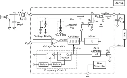
4.3.1 Carlson, E., Strunz, K., Otis, B. A 20 mv input boost converter with efficient digital control for ther- moelectric energy harvesting . . . 31
xiii
4.3.2 Ramadass, Y., Chandrakasan, A.A batteryless ther- moelectric energy-harvesting interface circuit with
35mv startup voltage . . . 32
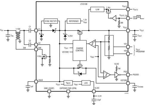
4.3.3 Doms, I., Merken, P., Mertens, R., Van Hoof, C. Integrated capacitive power-management circuit for thermal harvesters with output power10to1000µw 35 4.3.4 Linear Technology Ultralow voltage step-up con- verter and power manager (LTC3108) . . . 36
4.3.5 Chen, P.H., Ishida, K., Zhang, X., Okuma, Y., Ryu, Y., Takamiya, M., Sakurai, T. 0.18-v input charge pump with forward body biasing in startup circuit using65nm cmos . . . 38
4.4 Power Converters for Photovoltaic Transducers . . . 40
4.4.1 Chew, K.W.R., Sun, Z., Tang, H., Siek, L.A400nW single-inductor dual-input-tri-output DC-DC buck- boost converter with maximum power point tracking for indoor photovoltaic energy harvesting . . . 40
4.5 Future Prospects for Energy Harvesting Power Man- agement Circuits . . . 42
5 e n e r g y h a r v e s t i n g b o o t s t r a p p e d b o o s t r e g u l at o r 43 5.1 Introduction . . . 43
5.2 Proposed Circuit Topology . . . 44
5.2.1 Comparison to Previous Works . . . 44
5.2.2 Design Methodology . . . 44
5.2.3 Synchronous Boost Topology . . . 45
5.2.4 Design Methodology . . . 46
5.2.5 Block Diagram . . . 46
5.3 Startup . . . 47
5.3.1 Startup Charge Pump . . . 47
5.3.2 Startup Oscillator and Driver . . . 49
5.4 Steady-State Operation . . . 50
5.4.1 Hysteretic Control . . . 50
5.4.2 Output Voltage Ripple . . . 51
5.4.3 Maximum Load Current . . . 53
5.4.4 Voltage Hysteresis Value . . . 53
5.4.5 Voltage Reference . . . 54
5.5 Simulation Results . . . 57
5.5.1 Simulation Schematic . . . 57
5.5.2 Startup Results . . . 57
5.5.3 Steady State Results . . . 60
5.5.4 Calculation and Simulation Comparison . . . . 60
5.5.5 Efficiency . . . 61
5.6 Efficiency Analysis . . . 62
5.6.1 Design Optimizations . . . 63
5.7 Test Chip . . . 64
5.7.1 Chip Photomicrograph . . . 64
c o n t e n t s xv
5.7.2 Chip Packaging . . . 64
5.7.3 Bench Results . . . 64
5.7.4 Bench and Simulation Comparison . . . 66
5.8 Conclusion . . . 68
5.9 Future Work . . . 68
iii a p p e n d i x 69 a m u lt i p h a s e b u c k o u t p u t i m p e d a n c e 71 a.1 Background . . . 71
a.1.1 Impedance . . . 72
a.1.2 Multiphase Buck Regulator . . . 74
a.2 Buck Regulator Output Impedance . . . 75
a.3 Lab Setup . . . 76
a.3.1 Transconductance Amplifier . . . 76
a.3.2 Frequency Response Analyzer Settings . . . 78
a.4 Measurement Results . . . 78
a.4.1 Disabled Response . . . 79
a.4.2 Single Phase Output Impedance . . . 80
a.4.3 Output Impedance as a Function of Number of Phases . . . 80
a.4.4 Measured Load Transient Response . . . 81
a.5 Compensation Effect on Output Impedance . . . 82
a.6 Future Work . . . 83
b i b l i o g r a p h y 85
Figure2.1 Simplified linear regulator schematic. . . 5
Figure2.2 Linear regulator schematic with load. . . 6
Figure2.3 Low dropout regulator. . . 8
Figure2.4 Ideal switches. . . 8
Figure2.5 Conceptual buck regulator. . . 9
Figure2.6 Buck regulator steady-state timing diagram. . 10
Figure2.7 Conceptual boost regulator. . . 11
Figure2.8 Conceptual synchronous buck regulator. . . 13
Figure2.9 Conceptual synchronous boost regulator. . . . 13
Figure2.10 Practical implementation of a synchronous buck regulator. . . 14
Figure2.11 Practical implementation of a synchronous boost regulator. . . 15
Figure3.1 Conceptual energy harvesting system block di- agram. . . 19
Figure3.2 LDT0-028K piezoelectric transducer. . . 20
Figure3.3 LDT0-028K piezoelectric transducer resonant frequency. . . 21
Figure3.4 CUI CP85-series thermoelectric generator. . . . 21
Figure3.5 CUI CP85138Thermoelectric Generator (TEG) performance. . . 22
Figure3.6 Typical photovoltaic cell I-V characteristic. . . 23
Figure4.1 Block diagram of piezoelectric energy harvester in [2]. . . 26
Figure4.2 Bias-flip rectifier block diagram from [3]. . . . 27
Figure4.3 Full block diagram from [3]. . . 27
Figure4.4 Split-capacitor based AC-DC converter from [4]. 28 Figure4.5 Maximum energy harvesting scheme from [4]. 28 Figure4.6 Complete energy harvesting interface circuit from [5]. . . 29
Figure4.7 MOSFET full-wave rectifier in [5]. . . 30
Figure4.8 Block diagram of boost converter used in [8]. . 31
Figure4.9 Block diagram of circuit used in [9]. . . 33
Figure4.10 Startup circuit used in [9]. . . 33
Figure4.11 Energy storage circuit used in [9]. . . 34
Figure4.12 Block diagram of the circuit presented in [10]. 35 Figure4.13 Block diagram of LTC3108energy harvester in a TEG application. . . 37
Figure4.14 Internal circuitry of the LTC3108 energy har- vester. . . 37
Figure4.15 Three-stage Dickson type charge pump. . . 38
xvi
Figure4.16 Charge pump with forward body bias from [12]. 39
Figure4.17 Block diagram of the boost regulator in [12]. . 40
Figure4.18 Photovoltaic energy harvesting block diagram from [13]. . . 41
Figure5.1 Bootstrapped boost converter block diagram. . 46
Figure5.2 Startup charge pump oscillator. . . 48
Figure5.3 Full charge pump schematic. . . 49
Figure5.4 Startup oscillator and high duty cycle circuitry. 49 Figure5.5 Startup circuitry connected to drivers and out- put switches. . . 50
Figure5.6 Hysteretic control schematic. . . 50
Figure5.7 Hysteretic control state diagram. . . 51
Figure5.8 Constant-on-time voltage ripple analysis. . . . 52
Figure5.9 Banba bandgap voltage reference. . . 54
Figure5.10 Simulation schematic including parasitic resis- tances. . . 56
Figure5.11 Charge pump startup simulation. . . 58
Figure5.12 Steady state operation simulation. . . 60
Figure5.13 Efficiency over load range. . . 62
Figure5.14 Charge pump test chip. . . 64
Figure5.15 Packaged charge pump chip. . . 65
Figure5.16 Charge pump lab setup. . . 66
Figure5.17 Charge pump oscillator buffer output at400mV. 67 Figure5.18 Test chip transfer function with and without load. . . 67
Figure A.1 DA9210load transient response,1phase 2.8V. 72 Figure A.2 Impedance of ideal inductors and capacitors. . 73
Figure A.3 Multiphase buck regulator conceptual schematic. 74 Figure A.4 Multiphase buck current waveforms. . . 75
Figure A.5 Circuit to analyze open-loop output impedance of a buck converter. . . 75
Figure A.6 Output impedance lab setup block diagram. . 77
Figure A.7 Output impedance lab bench photograph. . . . 77
Figure A.8 Transconductance amplifier simplified schematic. 78 Figure A.9 Typicaldisabledimpedance response. . . 79
Figure A.10 Single phase output impedance response over VI N. . . 80
Figure A.11 Output impedance with a constant input volt- age but number of phases changed. . . 81
Figure A.12 Measured load transient response (0A→2A). . 81
xvii
Figure A.13 Output impedance based on compensation pole
trim code. . . 83
L I S T O F TA B L E S Table5.1 Transistor threshold voltageVt0 . . . 47
Table5.2 Simulation values . . . 56
Table5.3 Peak values in related works . . . 61
Table5.4 Charge pump test chip pinout. . . 65
Table A.1 Frequency response analyzer settings. . . 79
A C R O N Y M S A N D A B B R E V I AT I O N S
BJT Bipolar Junction Transistor CCM Continuous Conduction Mode
CMOS Complimentary Metal Oxide Semiconductor CTAT Complimentary To Absolute Temperature DCM Discontinuous Conduction Mode
DUT Device Under Test ESD Electrostatic Discharge
FRA Frequency Response Analyzer HD High Definition
LDO Low Dropout Regulator MCU Micro-Controller Unit
MIMCAP Metal Insulator Metal Capacitor MOS Metal Oxide Semiconductor
MOSFET Metal Oxide Semiconductor Field Effect Transistor MPP Maximum Power Point
MPPT Maximum Power Point Tracking NMOS n-type MOSFET
opamp Operational Amplifier PFM Pulse Frequency Modulation PMOS p-type MOSFET
PTAT Proportional To Absolute Temperature PWM Pulse-Width Modulated
RMS Root Mean Square SoC System on a Chip
SMPS Switch-Mode Power Supply TEG Thermoelectric Generator
TSMC Taiwan Semiconductor Manufacturing Company ZCS Zero Current Switching
xix
Part I
I N T R O D U C T I O N
1
B A C K G R O U N D
Over the last few decades, we have become obsessed with mobile devices. When the cell phone boom started in the 1990s, consumers were just starting to understand the value of always–on communica- tion systems, but now we can’t live without them. Parents need to keep in touch with their children, school kids need to keep in touch with their friends, and company employees need to receive urgent e–
mails from their bosses at any hour of the day or night. We have to be connected at all times—even1second of downtime is unacceptable.
But mobile devices are complicated systems, and they keep adding new features and increasing processor speeds. Each time a new fea- ture is added, or a faster processor is introduced, the power require- ments of the system increase. Yet to cut out features is tantamount to corporate suicide—consumers can’t live without High Definition (HD) video chatting, high-resolution3D games, video recording and high-speed web browsing from their smartphones. And since the competition is adding all these features, every smartphone manufac- turer feels the need to catch up or stay ahead.
These changing specs put increasing strain on power supply de- signers, who have to design their circuits to work with tighter tran- sient specs, at lower voltage, with much higher load currents. Failure to keep a regulated power supply for the System on a Chip (SoC) in these devices can lead to bit flips, kernel panics, and random restarts that completely ruin the user experience.
To make matters worse, consumers constantly complain about the battery life of their mobile devices. Even though this technology didn’t exist 10 years ago, a smartphone that won’t last all day without re- quiring recharging is considered useless. To address this perceived low battery life, power supply designers must also maximize the effi- ciency of their circuits; any small power loss is seconds of application time the user can’t utilize.
Because of the industry demands, and the ever-changing problems faced by the design of their circuits, I have dedicated my research to the study to power electronics for mobile devices. Within this field, energy harvesting is an up-and-coming area that shows great promise in raising our quality of life.
1.1 e n e r g y h a r v e s t i n g
Energy harvesting offers a chance to change the way we think about energy. By using transducers that capture energy from “free” sources
3
in the ambient environment, slight amounts of energy can be har- vested in order to power real systems.
There are many ways that micro-power transducers could be used in energy harvesting systems. A piezoelectric or vibrational trans- ducer attached to a bridge could be used to power a sensor grid. Ther- mal or vibrational transducers in implanted medical devices could re- duce the dependence on invasive surgeries used to change batteries.
Additionally, micro solar cells could be used to power watches or add power to cell phones.
In all of these examples, energy harvesting offers a way to reduce our dependence on conventional energy sources. If they are added to mobile devices, these systems could add trickle-charge to batteries and increase the amount of time a device can be used between charg- ing. While this effect will probably be transparent to the user, the increase in battery life can have a significant impact on the perceived quality of a mobile device.
2
S U R V E Y O F P O W E R M A N A G E M E N T C I R C U I T S R E L E VA N T T O M O B I L E A P P L I C AT I O N S
Power management circuits (orpower converters) are centered around creating a steady output voltage from a varying input source. A sim- ple example of a power management circuit is a microprocessor be- ing driven by a single-cell lithium battery, as is the case in modern cell phones. A single-cell battery typically has a voltage of 2.4 V at minimum charge to5.5V at maximum. Unfortunately, since the pro- cessor runs at a voltage around1.0V and uses a fine Complimentary Metal Oxide Semiconductor (CMOS) process, powering this chip di- rectly with a 5.5V supply will destroy the chip. In order to address this limitation, some type of power conversion circuit must be added between the battery and the microprocessor that delivers a constant 1.0V no matter what changes with the input voltage or load current.
2.1 l i n e a r r e g u l at o r s
One way of addressing this constant output voltage requirement is via a simple Operational Amplifier (opamp) and a large output tran- sistor as shown in Fig. 2.1. Using the fact thatVP =VN in theopamp, the DC transfer function can be written as in (2.1).
VO =
1+ R2 R1
VREF (2.1)
By selecting a suitable reference voltage and tuning the feedback resistors to a proper ratio, the output voltage can be adjusted to any value that is desired. Additionally, as long as theopampcan control the feedback loop and the system is stable, the output voltage will
− +
+−
V
REFV
IV
OR
1R
2Figure2.1: Simplified linear regulator schematic.
5
be well regulated at its set value. This type of power management circuit is known as alinear regulatordue to the analog, linear control implemented using an operational amplifier.
Note that in this simple example, an NPN Bipolar Junction Tran- sistor (BJT) is used at the output. This output transistor is commonly implemented with an n-type MOSFET (NMOS), though an NPN is shown for its relative simplicity. In general, this output transistor only acts as a unity-gain current buffer and should be a large enough size (and with a large enough heat-sink, if required) to handle the maxi- mum load current of the system.
2.1.1 Power Loss and Efficiency
While the linear regulator shown in Fig.2.1 is a simple circuit to im- plement, it generally suffers from high power loss and low efficiency.
Consider the situation in Fig. 2.2 where the regulator is feeding a constant load IO. In this case, the power delivered to the load is
PO =VOIO. (2.2)
Ignoring the quiescent power consumed by the opamp, the input power is
PI ≈VIIO. (2.3)
Thus, the efficiency of this circuit can be written as
η= PO PI ≈ VO
VI
. (2.4)
As an example, assume that the linear regulator is running from a5V input voltage, delivering2A of power to a1.0V load. In this case the efficiency is:
η≈ 1V5V =20%. (2.5)
− +
+−
V
REFV
IV
OR
1R
2I
OLD
Figure2.2: Linear regulator schematic with load.
2.1 l i n e a r r e g u l at o r s 7
While low efficiency is certainly an issue, another problem with this linear regulator is that the power loss (seen over the output transistor) is
PLoss = (VO−VI)IO =4 V×2 A=8 W. (2.6) This power loss is converted to heat in the output transistor, and in a mobile application this would create too much heat which could not be properly dissipated.
2.1.2 Low Dropout Regulators
As mentioned in the previous section, the linear regulator of Fig.2.1 will regulate nicely as long as the control loop (governed by the opamp) is stable. In order to maintain this stability, the output tran- sistor must remain in the linear control region, hence (2.7) and (2.8)
must be satisfied. VBE(ON)is the
Base-Emitter voltage when theBJTis ON
VBE >VBE(ON) (2.7)
VCE(sat)is the Collector-Emitter voltage at which the BJTsaturates
VCE>VCE(sat) (2.8)
In order to accommodate these requirements, assuming that the operational amplifier can swing its output rail-to-rail, the maximum output voltage is
VO(max) =VI−VBE(ON). (2.9) Since VBE(ON) is usually around 0.7 V, even the maximum output voltage can lead to a significant power loss at higher currents. If the output voltage is set to less than VO(max), the power loss across the output transistor will be even higher.
One way to minimize this power loss (and improve efficiency) is to use a PNP output transistor as shown in Fig.2.3. While this approach will still have a power loss across the output transistor, the maximum output voltage is now higher because
VO(max) =VI−VEC(sat). (2.10) Since the saturation voltage of the PNPBJT (labelledVEC(sat)) is only on the order of0.2V, this lower voltage appearing across the output transistor also leads to a lower power loss. The minimum voltage allowed between the input and output voltage in a linear regulator is
V
REFV
IV
OR
1R
2−
+ +
−
I
OLD
Figure2.3: Low dropout regulator.
called thedropout voltage, and hence the circuit of Fig.2.3is called a Low Dropout Regulator (LDO).
Note that switching the output transistor to a PNP also requires changing the inputs to the opamp since the PNP is operated as a common-emitter inverting amplifier. Additionally, by adding a final gain stage and the output transistor, the control loop varies consid- erably depending on the output load. Because of this issue, LDOs tend to be difficult to stabilize over a wide operating range, and care- ful attention needs to be paid to the opamp (control circuitry) and compensation network design.
Also like before, LDOs are commonly implemented using p-type MOSFET (PMOS) output transistors, but a PNP is used in this ex- ample because it is easier to estimate the on-voltage and saturation voltage of Bipolar Junction Transistors.
2.2 s w i t c h i n g r e g u l at o r s
While the linear regulators described in the previous section work well and are suitable for a variety of applications, higher efficiency can be achieved by using switches, inductors and capacitors to reg- ulate an output voltage. The fundamental principle behind Switch- Mode Power Supply (SMPS) is that for an ideal switch, the power loss is always zero watts.
Fig.2.4aand Fig.2.4bshow ideal open and closed switches, respec- tively. For an open switch, the voltage across the switch can be any value but the current through is zero. Similarly, for a closed switch,
I + V -‐
(a) Open switch.
I + V -‐
(b) closed switch.
Figure2.4: Ideal switches.
2.2 s w i t c h i n g r e g u l at o r s 9
the current through the switch can be any value but the voltage across is zero. Because of this, an ideal switch will have no power loss be- cause
PLOSS=V×I =0 W. (2.11)
In practical regulators, non-ideal transistor switches are used, and as such there are a number of power losses related to non-ideal switches.
By utilizing switches, inductors and capacitors, high-efficiency con- verters can be created that step down the output voltage (buck con- verter), boost up the output voltage (boost converter) or both (buck- boost converter). A brief introduction to buck and boost converters will be presented in the next subsections.
2.2.1 Buck Converter
A buck converter is a step-down converter that creates an output voltage less than the input voltage. Due to its high efficiency, buck converters are widely used to power microprocessors, where a higher voltage like a battery or12V supply is stepped down to around1.0V to power the microprocessor.
Figure2.5shows a conceptual buck regulator schematic. The buck regulator requires that the output voltage is less than the input volt- age, which can be seen by analyzing the circuit. SwitchSis generally operated with a fixed period and a duty cycle D. Inspecting the cir- cuit, we notice that the inductor L and capacitor C form a simple second-order low-pass circuit, and because of this, the output voltage is the average of the input voltage (as long as the inductor current stays positive).
For a more mathematical analysis of the buck converter, consider the timing chart in Fig. 2.6. Assuming the diode is ideal and the con- verter operates in Continuous Conduction Mode (CCM), i.e. the in- ductor current is always positive, steady-state operation means that the inductor current value does not change over one full cycle. Math- ematically, this can be expressed as:
V
IL
C S
D
V
OI
OLD
Figure2.5: Conceptual buck regulator.
t0 t1 t2 ton toff
v
O(t)
i
L(t)
V
OFigure2.6: Buck regulator steady-state timing diagram.
iL(t0) =iL(t2) (2.12)
Which implies that Z t1
t0
iL(t)dt+
Z t2
t1 iL(t)dt=0. (2.13)
At this time, it is convenient to note that, for an inductor charging with a constant voltage, we can use the relation
L∆I =V∆t. (2.14)
Note that (2.14) is the inductor equivalent of the well-known C∆V = I∆t used in analog circuit design to model a capacitor charged with a constant current. By inspecting the circuit and using the simplifica- tion of (2.14), we see that (2.13) can be re-written as
(VI−VO)L×ton+VOL×to f f =0. (2.15) Equation (2.15) is known as theinductor volt-second balanceequation, since the terms on the left and right consist of the voltage across the inductor multiplied by the amount of time the inductor charges (or discharges). This equation can be re-written in the more compact and well-known form
VO
VI =D (2.16)
whereDis the Duty Cycleof the Pulse-Width Modulated (PWM) sig- nal applied to control the switch (D=ton/TandT= ton+to f f). Thus, as suggested earlier, the buck regulator acts like a low-pass filter and the output voltage is the average of the switching waveform.
2.2 s w i t c h i n g r e g u l at o r s 11
2.2.1.1 Buck Converter Addendum
There are a number of subtle points that should be elucidated for the Buck converter.
First, the buck converter can run at100% duty cycle. In this situa- tionD=1 and hence the output voltage is equal to the input voltage.
In practical applications, there are times when 100% duty cycle op- eration is useful. Leaving switch S ON will not cause the inductor current to saturate or cause any other undesired behavior, since the input and output voltages will be equal.
Second, since the buck converter’s LandC act as a low-pass filter, the output voltage rises (slightly) during the switch ON time, but falls back down during the switch OFF time. This somewhat subtle effect is shown in Fig. 2.6.
2.2.2 Boost Converter
Another basic switching converter is theboost converterwhich creates an output voltage larger than the input voltage. The schematic of a basic boost converter is shown in Fig. 2.7.
Unlike the buck circuit, the boost converter is a bit more difficult to understand just by inspecting the circuit. The boost regulator works by charging the current in the inductor L during the on-time, then discharging this current into the output capacitor and load during the off-time. By completing the mathematical analysis, it can be seen that the output voltage will always be higher than the input voltage. In fact, if the switch is never commutated, the inductor can be modeled as a short circuit, and the output voltage will equal the input voltage (assuming the diodeDis ideal).
By utilizing the Inductor Volt-Second Balance approach used to de- rive (2.15), a similar expression can be obtained for the boost con- verter.
VIL×ton+ (VI−VO)L×to f f =0 (2.17)
V
IL
C S
D V
OI
OLD
Figure2.7: Conceptual boost regulator.
which can be rearranged as VO
VI = 1
1−D. (2.18)
For a boost converter, (2.18) is the most common way to write the DC transfer function. This equation shows that when the circuit doesn’t switch (D = 0), the output voltage will equal the input volt- age, while at higher duty cycle the output voltage will increase.
2.2.2.1 Boost Converter Addendum
The preceding analysis of the boost converter shows that the output voltage is always higher than the input voltage, and will increase in- finitely if the duty cycle reaches 100% (D = 1). Practically however, this is not the case. At 100% duty cycle, the boost converter’s switch will always be ON, meaning that current will continually build up in the inductor. In a practical circuit, there is a limit to the maximum current that the switch and inductor can handle before failure, and hence 100% duty cycle is not feasible. Practically, the output voltage at 100% duty cycle will also decrease, and the transfer function will actually reach zero. Because of this fact, it is very important to en- sure that the switch in a boost regulator always turns OFF for some amount of time, causing the output voltage to rise. Additionally, par- asitic components in a boost regulator have a large impact on the DC transfer function and on the overall performance of the circuit.
Because of these two issues, even when performing a simple circuit simulation, parasitic resistances and practical components should be added whenever possible. Moreover, circuitry that guarantees that the switch turns OFF for some amount of time must also be implemented.
2.2.3 Synchronous Switch Topology
The buck and boost converter circuits shown previously are asyn- chronous circuits, i.e. they require a diode to function, and the in- ductor current will hit zero amperes if the load current is too low.
In portable applications however, thesynchronoustopology is usually employed. With an asynchronous regulator, if the inductor current drops to zero for some time, the circuit operates in Discontinuous Conduction Mode (DCM). While this is useful in some applications, discontinuous conduction mode is not commonly used in portable applications. Instead, the synchronous switch topology utilizing a sec- ond switch (replacing the diode) is used. A simplified synchronous buck converter circuit is shown in Fig.2.8.
By adding a second switchS2, the inductor current can now flow in the negative direction, meaning that current flows up from ground, throughS2, and to the output capacitor/load. Because of this feature,
2.2 s w i t c h i n g r e g u l at o r s 13
V
IL
C S
1S
2V
OI
OLD
Figure2.8: Conceptual synchronous buck regulator.
even when the load is 0A, the circuit will act as though it is still operating in continuous conduction mode, though now the inductor current can swing negative.
Similar to the synchronous buck converter, a simplified synchronous boost converter is shown in Fig. 2.9. Like the case of the buck con- verter, switch S2 now takes the function of the diode in the asyn- chronous circuit. During the ON time, switch S1 will be ON and charging the inductor current. During the off time, switch S1 turns off and S2 turns on, hence current built up in the inductor is trans- ferred to the output capacitor and load throughS2.
2.2.3.1 Synchronous Topology Advantages
The previous discussion has assumed that diodes are ideal. Practi- cally, in an asynchronous converter like the buck circuit in Fig 2.5, the inductor current will discharge through the diode D during the off-time. This discharge will also lead to a power loss of
PLOSS=VD(on)×I (2.19)
where I is the Root Mean Square (RMS) value of the current flowing through the diode during this time, andVD(on)is the‘on’ voltageof the diode. In applications where the current that flows through the diode is fairly small, this power loss is negligible. In mobile devices however, there is usually a large output current, hence using a diode would
V
IL
C S
1S
2V
OI
OLD
Figure2.9: Conceptual synchronous boost regulator.
have a large effect on the efficiency of the system. Because of this, a synchronous topology is used in most portable power applications.
2.2.3.2 Practical Implementation
Since ideal switches and diodes don’t exist in the real world, the switches shown in Fig. 2.8 are generally implemented with PMOS andNMOStransistors, as shown in Fig.2.10.
To a decent approximation, a Metal Oxide Semiconductor Field Ef- fect Transistor (MOSFET) that is “OFF” is truly off, and no current flows through the channel. When a MOSFET is ON however, there is some conduction loss due to the fact that the channel has a finite resistance. Using the well-known triode MOSFET equation and ap- proximating forVDS being very small, an equation can be derived for thison resistanceof theMOSFET.
rDS(on)≈ 1
k0WL(VGS−Vt) (2.20)
Note that in (2.20), the variables W and L correspond to the gate width and length of the transistor, respectively. Hence, it can be seen that increasing the width of the MOSFET or increasing the gate-to- source voltage will reduce the on resistance. In a battery-powered application, the gate-source voltage of the MOSFET is usually fixed to the battery voltage, meaning that, practically, only the transistor width can be increased to lower the on-resistance.
The factork0 is known as theprocess parameterand is based on the type of process used to make these MOSFET transistors. While the full derivation of this variable is beyond the scope of this manuscript, it is interesting to note that for anNMOS, the value of k0 is2-3times larger than that of aPMOS. Due to this discrepancy, thePMOSis gen-
This is due to the fact that electrons (n-ch) move faster than holes (p-ch)
erally designed with a width2-3times larger than itsNMOScounter- part, ensuring that bothNMOSandPMOShave identical (or nearly- identical) on-resistance.
While mathematically it seems that increasing the transistor width, or increasing theW/Lratio infinitely would be ideal, there are a num- ber of other issues to consider. First, a larger transistor takes up more
V
IL
C S
PS
NV
OI
OLD
Figure2.10: Practical implementation of a synchronous buck regulator.
2.3 s u m m a r y 15
V
IL
C S
PS
NV
OI
OLD
Figure2.11: Practical implementation of a synchronous boost regulator.
chip area, which is especially problematic as die size shrinks smaller and smaller. Additionally, increasing the transistor size increases the gate capacitance, meaning that drivers must be made larger, while in- creasing the amount of dynamic switching losses from the transistors.
In typical applications, there is a set size for power transistors or a minimum-allowable value ofrDS(on)which engineers design around.
Similar to the buck converter, a synchronous boost converter can also be implemented usingMOSFETsas shown in Fig.2.11. While the MOSFETsthemselves function similarly to the ideal switches shown in the previous boost regulator of Fig.2.9, special attention should be paid to the gate driving voltage of these transistors. During the ON time, switch SN is turned on, which can be accomplished by putting a large voltage (i.e. VI N) at the gate of SN. In order to keep SP off during this time however, the source-to-drain voltage must be zero, hence the gate of SN must be tied to the output voltage (which is higher than VI). Notice that for the buck regulator this was not an issue—if the gates of both SN and SP switch between zero and VI N, this is enough to turn the transistors ON or OFF.
While Metal Oxide Semiconductor (MOS) transistors aren’t ideal switches (and will contribute to power loss in the system), they are good enough for many applications and have found wide adoption in power management circuits for mobile applications. As long as the process being used can tolerate an input voltage of about5V, almost any CMOS process can be used to implement power transistors. Of course, better processes will add mask layers to reducerDS(on), reduce sensitivity to Electrostatic Discharge (ESD)/latchup or optimize other parameters that are important to power management circuits.
2.3 s u m m a r y
This chapter has given a basic overview of power management cir- cuits, including linear and switching regulators. Power management is a vast field where multiple textbooks are required to fully under- stand the principles and applications of all types of power converters.
But for the purposes of this dissertation, it is hoped that the explana-
tions in this chapter give a decent introduction to power converters that are used in mobile applications.
Subsequent chapters introduce more complicated concepts in power management. In order to not overwhelm the reader, however, those explanations are written in their respective chapters.
Part II
T O P I C S I N E N E R G Y H A R V E S T I N G
3
S U R V E Y O F E N E R G Y H A R V E S T I N G T R A N S D U C E R S
3.1 b a c k g r o u n d
Energy harvesting represents a new way of thinking about energy.
Instead of relying on power sources with limited supplies or severe drawbacks like gas or nuclear power plants, energy can be captured from ambient sources in our natural environment. There are a num- ber of different types of energy harvesting transducers, and each could be used in different practical applications.
A piezoelectric or vibrational transducer attached to a bridge could be used to power a sensor grid. Micro solar cells could be used to power watches or add power to cell phone batteries, even when pow- ered from relatively weak fluorescent lighting. Furthermore, thermal or vibrational transducers in implanted medical devices could reduce the dependence on invasive surgeries used to change batteries.
A typical system used in energy harvesting systems is shown in Fig. 3.1. The energy harvesting transducer is fed into some kind of battery management circuit (usually a boost converter) which stores harvested energy on some kind of energy storage component (battery, super-capacitor, etc). This stored energy can then be transferred to the system power supply (another power management circuit) which then drives a Micro-Controller Unit (MCU) and some kind of wireless interface circuit.
A good example of this energy harvesting system is a remote sens- ing network on a bridge. Natural vibrations of the bridge cause piezo- electric transducers to gather a small amount of energy, which helps
Energy Harvester
Thermal Solar Vibra6onal RF Harves6ng
Etc.
Boost Converter /
Ba>ery Management System Power
MCU
Wireless Interface ZigBee, etc Energy Storage
Figure3.1: Conceptual energy harvesting system block diagram.
19
charge a battery. The energy stored in this battery can then be used to feed a low-power wireless network that reports the sensor readings periodically back to a main server. This wireless transmission can be performed with aburstingtype of control, i.e. the transceiver is only active for a short amount of time (on the order of 1 ms per hour).
This approach helps to lower the amount of power required by the system and ensures that the transceiver and MCU do not consume more power than the energy harvesting transducer can provide.
However, one drawback with conventional energy harvesting ap- proaches is that they require a battery as a storage element. While battery chemistry gets better every year, there is still no battery that lasts forever, and in these systems the batteries would still need to be replaced at regular intervals.
3.2 t y p e s o f e n e r g y h a r v e s t i n g t r a n s d u c e r s
Focusing on the block diagram in Fig. 3.1, there are a number of dif- ferent types of energy harvesting transducers that can be used. The most common of these arePiezoelectric Transducers,Thermoelectric Gen- erators andPhotovoltaic Transducers. Details about each of these three types of transducer are described in the following subsections.
3.2.1 Piezoelectric Transducers
Piezoelectric transducers generate electrical energy from vibrational energy. In practical applications, these transducers would be placed on some kind of structure that vibrates, like a bridge or a rotating piece of machinery. Vibrational transducers operate at a certain reso- nant frequency which can be changed by altering the effective length of the transducer or changing the position of a tuning mass.
One type of vibrational transducer is the LDT0-028K from Measure- ment Specialties [1] shown in Fig.3.2. With this transducer, the large tuning mass shown on the left side can be altered in order to change the resonant frequency of the transducer. A larger tuning mass cor-
Figure3.2: LDT0-028K piezoelectric transducer.
3.2 t y p e s o f e n e r g y h a r v e s t i n g t r a n s d u c e r s 21
Figure3.3: LDT0-028K piezoelectric transducer resonant frequency.
responds to a lower resonant frequency while no tuning mass corre- sponds to a resonant frequency of about180Hz, as shown in Fig.3.3. Since piezoelectric transducers are connected to some kind of vi- brating source, the output of the transducer is an AC signal, and hence any power management circuits that convert this to a usable voltage will have to convert the AC signal into a DC signal. There are a number of prior works [2–5] that have investigated energy harvest- ing for piezoelectric systems. Details about each of these approaches will be presented in Section4.2.
3.2.2 Thermoelectric Generators
A Thermoelectric Generator (TEG) is operated by exploiting the See- beck effect, where an electrical signal is created if the junctions of two different conductors are held at different temperatures. Using this physical property, injecting current into a TEG can cause it to cool down, which is used in many industrial applications. Conversely, let-
page date DESCRIPTION: application notes
1 of 8 01/2009
20050 SW 112th Ave. Tualatin, Oregon 97062 phonephone 503.612.2300 faxfax 503.612.2382 PART NUMBER: CP Series
APPLICATION NOTES
1. PELTIER HISTORY
Early 19th century scientists, Thomas Seebeck and Jean Peltier, first discovered the phenomena that are the basis for today’s thermoelectric industry. Seebeck found that if you placed a temperature gradient across the junctions of two dissimilar conductors, electrical current would flow. Peltier, on the other hand, learned that passing current through two dissimilar electrical conductors, caused heat to be either emitted or absorbed at the junction of the materials. It was only after mid-20th Century advancements in semiconductor technology, however, that practical applications for thermoelectric devices became feasible. With modern techniques, we can now produce thermoelectric “modules” that deliver efficient solid state heat-pumping for both cooling and heating; many of these units can also be used to generate DC power at reduced efficiency. New and often elegant uses for thermoelectrics continue to be developed each day.
2. PELTIER STRUCTURE
A typical thermoelectric module consists of an array of Bismuth Telluride semiconductor pellets that have been “doped” so that one type of charge carrier– either positive or negative– carries the majority of current. The pairs of P/N pellets are configured so that they are connected electrically in series, but thermally in parallel.
Metalized ceramic substrates provide the platform for the pellets and the small conductive tabs that connect them.
3. PELTIER THEORY
When DC voltage is applied to the module, the positive and negative charge carriers in the pellet array absorb heat energy from one substrate surface and release it to the substrate at the opposite side. The surface where heat energy is absorbed becomes cold; the opposite surface where heat energy is released, becomes hot. Reversing the polarity will result in reversed hot and cold sides.
Ceramic Substrate
P-Type Semiconductor
Pellets Conductor
Tabs N-Type
Semiconductor Pellets Positive (+)
Negative (-)
FIGURE 1. CONSTRUCTION
Released Heat
N-TYPE BISMUTH TELLURIDE
P-TYPE BISMUTH TELLURIDE
Released Heat
Absorbed Absorbed Heat
Heat
DC POWER SOURCE FIGURE 2. THEORY
Figure3.4: CUI CP85-series thermoelectric generator.
22 s u r v e y o f e n e r g y h a r v e s t i n g t r a n s d u c e r s
!"#!"#$
ΔT=Th−Tc(℃)
0
0 4.0 8.0 1.0 2.0
Heat Pumped (W)Input Voltage (V)
8.5 A
6.8 A
5.1 A
3.4 A
1.7 A
8.5 A
6.8 A 5.1 A 3.4 A
1.7 A
CP85138 PERFORMANCE (Th=27°C)
ΔT=Th−Tc(℃)
0
0 4.0 8.0 1.0 2.0
Heat Pumped (W)Input Voltage (V)
8.5 A
6.8 A
5.1 A
3.4 A
1.7 A
8.5 A
6.8 A 5.1 A 3.4 A
1.7 A
CP85138 PERFORMANCE (Th=50°C)Figure3.5: CUI CP85138TEGperformance.
ting both sides of the TEG reach different temperatures will create an electrical signal, which can be used with an energy harvesting cir- cuit to power a useful system. In modern TEGdesign, n- and p-type silicon can be used to create electrical power from a temperature dif- ference.
Fig.3.4shows the internals of the CP85-series thermoelectric gener- ators from CUI [6]. Depending on the voltage and amount of current applied to theTEG, the temperature difference of theTEGcan be con- trolled [7] as shown in Fig. 3.5. While this figure shows the situation when power is applied to the Peltier cooler in order to change the temperature, the opposite is also true and using the TEGas a power source will work as long as there is a temperature difference across both sensor terminals. Although the value is not shown explicitly in Fig.3.5, operating theTEGwith a small temperature difference is able to generate a small voltage (ca.500mV) with a fairly large current.
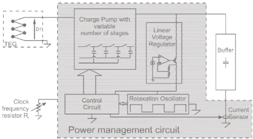
The output of a thermoelectric transducer is a DC voltage, which simplifies the design in creating power management circuits that are capable of driving a realistic and useful load. A number of prior works [8–11] , all of which aim to lower the minimum voltage at which the power converter can operate. A detailed description of each of these circuits will be presented in Section4.3
The output voltage of a TEG seems to vary greatly based on the materials used and the number of devices (or semiconductor voltage generators) placed together in series or parallel. Some transducers have an output voltage in the range of 5 mV / ◦C [8], while others generate a voltage of several hundred millivolts even with a small
![Fig. 3 . 4 shows the internals of the CP 85 -series thermoelectric gener- gener-ators from CUI [ 6 ]](https://thumb-ap.123doks.com/thumbv2/123deta/6240190.1092405/42.892.248.745.99.461/fig-shows-internals-series-thermoelectric-gener-gener-ators.webp)
![Figure 4 . 4 : Split-capacitor based AC-DC converter from [ 4 ].](https://thumb-ap.123doks.com/thumbv2/123deta/6240190.1092405/48.892.249.743.105.305/figure-split-capacitor-based-ac-dc-converter.webp)
![Figure 4 . 17 : Block diagram of the boost regulator in [ 12 ].](https://thumb-ap.123doks.com/thumbv2/123deta/6240190.1092405/60.892.253.738.117.440/figure-block-diagram-boost-regulator.webp)