Study on Growth and Characteristics of Thermally Evaporated Organic Semiconductor Layers
(
加熱蒸着した有機半導体層の成長と特性に関する研究
)July 2018
Doctor of Engineering
Aye Myint Moh
Toyohashi University of Technology
別紙4-1(課程博士(英文))
Date of Submission(month, day, year): 7.9.2018 Department
Mechanical Engineering Student ID Number D 159105
Supervisors
Izaki Masanobu
Seiji Yokoyama
Applicant’s name Aye Myint Moh
Abstract ( Doctor )
Title of Thesis
Study on Growth and Characteristics of Thermally Evaporated Organic Semicon-
ductor Layers (加熱蒸着した有機半導体層の成長と特性に関する研究)
Approx. 800 words
The organic semiconductors have been employed in electronics and optoelectronic devices be- cause of their wide range of properties. A great number of organic materials have been used as the active layer for applications in organic electronics such as organic light emitting diodes (OLEDs), organic field effect transistors (OFETs), and organic photovoltaic devices (OPVs). Organic layers have been prepared by using several methods of solution process such as spin-coating, and vacuum process such as vacuum thermal evaporation. The structure and quality of the resultant organic layers affects the performance of the electronic devices, and the amorphous and bulk-heterojunction struc- ture that was a nano-scale mixture of the n-type and p-type organic semiconductor have been em- ployed for organic PV devices.
Organic semiconductors of π-conjugated small molecules are promising and versatile organic semiconductors for the electronics and optoelectronic devices including organic PV devices because of the high mobility relating to the diffusion length of the carrier. The transporting phenomena of the mobility is affected by the molecular arrangement in the organic semiconductor layers, and the arrangement of the thin layers installed into the devices has been controlled by adjusting the growth including the preparation technique, substrate and under-layer material, and the deposition rate. The heteroepitaxial growth has been generally employed for the fabrication of electronics and optoelec- tronics devices constructed of inorganic semiconductors, and the lattice relationship at the hetero- interface between the layer and substrate material affects the atomic arrangement of the resultant inorganic layer. The information and knowledge on the growth of organic semiconductors is still insufficient compared with that for inorganic semiconductors.
In this thesis, the structure of single layers and bi-layers of π-conjugated small molecules of 2,7- dioctyl[1]benzothieno[3,2-b][1]benzothiophene (C8-BTBT) and N,N'-dioctyl-3,4,9,10- perylenedi- carboximide (PTCDI-C8) prepared on single crystal substrates by a vacuum thermal evaporation was investigated with X-ray diffraction (XRD) and atomic force microscopy (AFM). The purpose of this work is to characterize the growth of organic semiconductors including the effects of the under-layer material and orientation and to propose the tentative growth model applicable for the development of next generation p-conjugated small molecular based devices.
In Chapter 1, the background and purpose of this study was mentioned.
In Chapter 2, the preferred orientation and growth behavior of C8-BTBT deposited on quartz glass, (1120)A-, (0001)C-, (1102)R-single-crystal Al2O3 (sapphire), (100)-, and (111)-single-crystal MgO substrates were investigated by XRD and AFM. The (001) out-of-plane orientation with a similar in-plane orientation was developed irrespective of the substrate material and orientation, and the degree of the development was reflected by the grain structure of the substrates.
In chapter 3, effects of the layer thickness and preparation temperature of the C8-BTBT layer on C-sapphire substrate on the growth and characteristics have been investigated with XRD, AFM, op- tical absorption measurement, and resistivity measurement with and without light irradiation. The C8-BTBT layers with the optical bandgap energy around 3.3 eV possessed the (001) out-of-plane
orientation irrespective of the layer thickness and preparation temperature. The C8-BTBT layers were growing up in direction parallel to the substrate surface keeping almost constant height, and the continuous layer was formed by the coalescence of the C8-BTBT grains. The electrical resistivity decreased with increase in the preparation temperature due to the increase in the grain size, and the light irradiation induce the drastic decrease to 42-28 Wcm. The tentative growth mechanism gov- erned by p-p-stacking-induced molecular ordering and diffusion of molecules on the substrates was proposed based on the experimental results.
In chapter 4, the preferred orientation and structure of PTCDI-C8 layers on the Al2O3 and MgO substrates were investigated by XRD and AFM observation. The (001) out-of-plane orientation was developed irrespective of the substrate material and orientation, and the continuous layer composed of needle-like grains was formed at the thickness of 15 nm followed by the grain growth with the thickness. The growth of the PTCDI-C8 layer was similar to that for C8-BTBT layer, and the pro- posed growth mechanism is adequate to the PTCDI-C8 growth.
In Chapter 5, the surface state of C8-BTBT/PTCDI-C8 bi-layers prepared on C-sapphire sub- strate were investigated by XRD, AFM, and Kelvin Force Microscopy (KFM). The lattice relation- ship of (001)-C8-BTBT//(001)-PTCDI-C8 was developed irrespective of the stacking order, but the C8-BTBT/PTCDI-C8 bi-layer showed an excellent performance in the surface morphology and po- tential homogeneity compared with the PTCDI-C8/C8-BTBT bi-layer, suggesting the importance of the stacking order in the fabrication of the bi-layer and the p-p-stacking-induced molecular ordering of each layer on the growth.
In Chapter 6, the results obtained in this study was summarized. The tentative growth mechanism proposed based on the experimental results was adequate to the growth of the single layers and bi- layers of C8-BTBT and PTCDI-C8, and the growth model and experimental results obtained here will support to the improvement of the performance of future π-conjugated based organic semicon- ductor layers and device fabrication for organic-based applications.
i
CONTENTS
CHAPTER 1: Introduction
1.1 Introduction to organic semiconductors 1
1.2 Structure of organic semiconductor devices 1.2.1 Organic Photovoltaics (OPVs) 7
1.2.2 Organic Field Effect Transistors (OFETs) 10
1.3 Importance of the growth control to enhance the performance 12
1.4 Growth of inorganic and organic thin films and preparation techniques for organic layers 1.4.1 General concepts of thin film growth 17
1.4.2 Preparation techniques for organic semiconductors and organic thin film growth 19
1.5 Organic semiconductor materials investigated in this work 22
1.6 Growth of organic molecules C8-BTBT and PTCDI-C8 26
1.7 Design of the growth of the C8-BTBT and PTCDI-C8 28
1.8 Research objectives 29
1.9 Outline of this study 31
REFERENCES 33
ii
CHAPTER 2: Growth of C8-BTBT molecules on inorganic single crystal substrates with various orientations
2.1 Introduction 46
2.2 Experimental procedures 48
2.3 Results and discussion 2.3.1 Effects of the substrate materials on the preferred orientation of the 48
C8-BTBT layers 2.3.2 Grain structure of the C8-BTBT layers prepared on the single crystal substrate 53
2.3.3 Tentative growth model of the C8-BTBT layer on single crystal substrates 55
2.4 Conclusions 56
REFERENCES 57
iii
CHAPTER 3: Growth and characteristics of C8-BTBT layers on C-sap- phire substrate by thermal evaporation
3.1 Introduction 61
3.2 Experimental procedures 63
3.3 Results and discussion 3.3.1 Orientation of the C8-BTBT layers prepared on C-sapphire substrate 64
3.3.2 Growth of the C8-BTBT layers on the C-sapphire substrate 67
3.3.3 Optical and electrical characteristics of the C8-BTBT layers 71
3.4 Conclusions 74
REFERENCES 75
iv
CHAPTER 4: Growth and characteristics of PTCDI-C8 layers on single crystal substrates with various orientations
4.1 Introduction 78
4.2 Experimental procedures 80
4.3 Results and discussion 4.3.1 Effects of the substrate material and orientation of the PTCDI-C8 layers 81
4.3.2 Orientation of the PTCDI-C8 layers on C-sapphire substrate 84
4.3.3 Grain structure and growth of the PTCDI-C8 layers 85
4.4 Conclusions 89
REFERENCES 90
v
CHAPTER 5: Fabrication and structure of PTCDI-C8/C8-BTBT bi-layer
5.1 Introduction 94
5.2 Experimental procedures 96
5.3 Results and discussion 5.3.1 Effects of the stacking sequence on preferred orientation of PTCDI-C8/C8-BTBT bi-layers 97
5.3.2 Surface homogeneity of the PTCDI-C8/C8-BTBT bi-layer 99
5.3.3 Growth model of the PTCDI-C8/C8-BTBT bi-layer 100
5.4 Conclusions 101
REFERENCES 102
vi
CHAPTER 6: Summary
6.1 Research summary 105
6.2 Acknowledgement 109
6.3 Research achievements 111
6.3.1 List of publications 111 6.3.2 List of conferences 112
1
CHAPTER 1
Introduction
1.1 Organic semiconductors
The organic semiconductors have a wide range of properties as thermal, physical, opti- cal, electrical, and magnetic characteristics which make them possible to be employed in large area, and lightweight electronics and optoelectronic applications.[1–5] Since impressive devel- opment in organic semiconductor materials as conductive halogen-doped polyacetylene with
2
conductivity up to 105 S/m have been discovered by Shirakawa, Heeger, and MacDiarmid, the research interest has been focused on the use of molecular based materials in electronics appli- cations.[6] The semiconducting properties of organic materials exhibit the π-conjugation sys- tem. This π-conjugated bonds in organic materials allow for electron delocalization along mol- ecule which give rise the semiconducting properties including conductivity and electronic be- haviors. By applying these concepts, it have been demonstrated that the suitability of organic semiconductor materials in a wide range of commercial devices including displays, smart tags, diodes, transistors, solar cells and sensors.[7–11] All of these electronic devices mainly based on organic layers which serve as the active layer. Since the quality of the active organic layers is directly linking to the performance of the devices, fabricating the organic layers with prom- ising organic materials and characterization of its formations are highly required for develop- ment of efficient devices.
The π-conjugated organic semiconductors are promising and versatile materials for electronics and optoelectronic devices.[12–15] Many research have been progressed and fo- cused on the development of high performance organic devices built from conjugated organic molecules because high efficient organic light-emitting diodes (OLEDs) was demonstrated by C.W. Tang and S. A. VanSlyke in 1987.[16] A great number of π-conjugated organic materials have been used for application in organic electronics; organic light emitting diodes (OLEDs), organic field effect transistors (OFETs), and organic photovoltaic devices (OPVs), etc.[5][17–
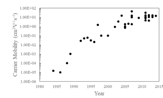
20] In general, charge transport property of charge carrier mobility is very important factor for these devices. It have been reported the comprehensive review of the progress in carrier mobil- ity of organic semiconductors with the year from 1984 to 2014 in Figure 1.1 and Table 1.1.[21][22]
3
Figure 1.1 Evolution of field-effect mobility value of organic semiconductor based TFTs.
Table 1.1 The reported results for highest field effect mobility values of organic semiconductor based TFTs 1984 to 2014.
Year Organic Semiconductors Deposition Method Mobility (cm2V-1s-1)
Refer- ence 1964 Cu-pthalocyanine Vacuum deposition Not Reported [23]
1983 Polyacetylene Solution process Not Reported [24]
1984 Merocyanine 1.5×10⁻⁵ [25]
1986 Polythiophene Solution process 10-5 [26]
1988 Polyacetylene
Poly(3-hexylthiophene) Phthalocyanine
Solution process Solution process Vacuum deposition
10-4 10-4
[27]
[28]
[29]
1989 Poly(3-alkylthiophene) α-sexithiophene
Solution process Vacuum deposition
10-3 10-3
[30]
[31]
4
1992 α-sexithiophene Pentacene
Vacuum deposition Vacuum deposition
0.027 2×10⁻³
[32]
1993 α- ω-dihexyl-sexithiophene Polythienylenevinylene
Vacuum deposition Solution process
0.05 0.22
[33]
[34]
1994 α- ω-dihexyl-sexithiophene Vacuum deposition 0.06 [35]
1995 α-sexithiophene Pentacene
Vacuum deposition Vacuum deposition
0.03 0.038
[36]
[37]
1996
1996
Phthalocyanine
Poly(3-hexylthiophene) Pentacene
Vacuum deposition Solution process Vacuum deposition
0.02 0.045 0.62
[38]
[39]
[40]
1997 Pentacene
Bis(dithienothiophene) trans-trans-2,5-Bis-[2-5-(2,2- bithienyl)ethenyl]thio- phene(BTET)
Vacuum deposition Vacuum deposition Vacuum deposition
1.5 0.05 0.01
[41]
[42]
[43]
1998 Poly(3-hexylthiophene) α- ω-dihexyl-quaterthiophene Dihexyl-anthradithiophene
Solution process Vacuum deposition
0.1 0.23 0.15
[44]
[45]
[46]
2000 α- ω-dihexyl-quinquethiophene Solution process 0.1 [47]
2002 Pentacene
N,N’-dioctyl-3,4,9,10-perylene tetracarboxylic diimide
(PTCDI-C8)
Solution process Vacuum deposition
0.89 0.6
[48]
[49]
2003 Pentacene Vacuum deposition 3.4 [50]
5
2004 Rubrene Single crystal 15 [51],[52]
2005 Rubrene Solution process 0.7 [53]
2006 2,7-Diphenyl[1]ben-
zothieno[3,2-b]benzothiophene (DPh-BTBT)
Vacuum deposition 2 [54]
2007 TIPS-pentacene Pentacene Rubrene
Hexamethlenetetrathiafulvalene (HMTTF)
titanyl phthalocyanine (TiOPc)
Solution process Single crystal Single crystal Single crystal
Vacuum deposition
1.8 15-40 43 10
10
[55]
[56]
[57]
[58]
[59]
2009 Dinaphtho[2,3-b:2’,3’- f]thieno[3,2-b]-thio- phene(DNTT)
Single crystal 8.3 [60]
2011 2,7-dioctyl[1]benzothieno[3,2- b][1]benzothiophene
(C8-BTBT) TIPS-pentacene C10-DNTT C10-DNTT
Dianthracen-[2,3-b:2’,3’f]
thieno[3,2-b]thiophene (DATT)
Single crystal, Solution process
Solution process Vacuum deposition Solution process Single crystal
31.3
4.6 8 11 16
[61]
[62]
[63]
[64]
[65]
6
2012 Hexacene C13-BTBT
Dithienylthieno(3,2-b)thiophene (DTT) and N-alkyl diketo- pyrrolo-pyrrole (DPP)
Single crystal Vacuum deposition Solution process
4.3 17.2 10.5
[66]
[67]
[68]
2013 TIPS-pentacene
Bis(benzothieno) naphthalenes (BBTN)
Solution process Vacuum deposition
11 15.6
[69]
[70]
2014 Poly (thineoisoindigo-alt-naph- thalene)(PTⅡG-Np)
Solution process 14.4 [71]
According to those charge carrier mobility values, progression is the development of designing and synthesis of new materials, deposition techniques and controlling the growth during deposition which make improving the interface between substrate-molecules and/or molecules-molecules.[42][72] The performance and efficiency analysis of the π-conjugated small organic molecular based devices have been emphasized since some devices including OFET based displays, radio frequency identification tag, OLED display and lighting were com- mercially available. However, some challenges still remain for good performance molecular based devices as the stability of the devices with high mobility. To fulfill these statements, the organic thin films with high crystallinity and less defect concentration are highly demanded.
7
1.2 Structure of organic semiconductor devices
The organic semiconductors are promising materials to be used in organic electronics and optoelectronics devices. [73–75] The different properties and structure of the organic mo- lecular layers determine the performance of the organic electronics devices. Different kinds of organic electronics and optoelectronics devices demand different properties of the layer struc- ture. For instance, highly order monocrystalline structure is particularly required for high per- formance organic field effect transistors (OFETs) and organic photovoltaic devices (OPVs).
[76–78] In contrast, amorphous structure with high uniformity and smooth surface formation is desirable for organic light emitting devices (OLEDs) because of the hopping-type charge trans- fer and highest quantum yield in amorphous structure layers.[79]
Different electronics and optoelectronics structure or configuration of devices required the different properties of semiconductor layers as molecular packing structure including mo- lecular orientation and grain structure within the organic active layers. Among the development of various molecular based electronic devices, two typical devices OPVs and OTFTs are de- scribed here.
1.2.1 Organic Photovoltaics (OPVs)
The organic semiconductor layers serve as active layers in organic photovoltaics OPVs devices and it convert light energy to electricity. OPVs could be fabricated by using different device structures including single layer cells, and layers stacking of organic active layers as heterojunction cells, tandem cells and so on. The single layer structure of OPVs showed poor performance with power conversion efficiency less than 0.1% before the mid1980s.[80] In 1986, efficiency improvement become 1% have been achieved by stacking the bi-layer of electron donor (D) and electron acceptor (A) as heterojunction type solar cells.[16] The molecular blend
8
type co-deposited bulk heterojunction solar cell was developed by Hiramoto et al.[81,82] The different configurations of heterojunction OPVs are shown in Figure 1.2.
Figure 1.2 Schematic diagrams of structure of OPVs (a) bi-layer planar heterojunction (b) bulk- heterojunction.
In heterojunction cells, donor layer and acceptor layer of photoactive layers were sand- wiched between two electrodes; cathode and anode. There are four basic principles (in Figure 1.3) for the operation of heterojunction OPVs. They are (1) light absorption and formation of excitons, (2) exciton diffusion to the donor-acceptor interface, (3) exciton dissociation, and (4) charge carrier transport and charge collection at the electrodes. [83]
When the solar spectrum is directed onto the organic semiconductor layer and absorp- tion of photons which lead to the electron-hole pairs of excitons formation in the first step of the operations. After absorption of light, photo generated excitons diffuse inside the layer within a few nanometer range 5-20 nm.[84] Since the exciton diffusion length in organic semiconduc- tor have a limitation, it is required for exciton to reach a donor-acceptor interface. Exciton dis- sociation occurs at the donor-acceptor interface when the difference in energy level of LUMO
9
of donor and acceptor is higher than exciton binding energy. Exciton recombination may hap- pen when excitons do not reach the donor-acceptor interface, and in this case, photocurrent could not be generated. Exciton dissociation is one of the crucial steps for performance of the OPVs which is affected by the interface structure as the planar heterojunction or bulk hetero- junction. The excitons require to dissociate at the donor-acceptor interface in order to collect the charge at the electrodes. It is clearly seen that these process of the OPVs are affected by the structure including orientation, morphology, and grain structure of the donor-acceptor lay- ers.[17][85]
Figure 1.3 Schematic diagram of basic principles for the operation of heterojunction OPVs (1) light absorption and formation of excitons, (2) exciton diffusion to the donor-acceptor interface, (3) exciton dissociation, and (4) charge carrier transport and charge collection at the electrodes.
10
1.2.2 Organic Field Effect Transistors (OFETs)
Organic Field Effect Transistors are fundamental building block for electronic devices as displays, sensors, radio frequency identification tags and so on.[9,10][86,87] Generally, OFETs can be fabricated by three basic layers (1) Organic semiconductor layer (2) three-elec- trodes (gate, source and drain), and (3) an insulating layer. Four basic types of conventional OFETs device structures are shown in Figure1.4.
Figure 1.4 Schematic diagrams of typical structure of FETs (A), (B) Bottom-gate, and (C), (D) Top-gate.
Basically, two ohmic contacts of the source and drain electrodes are stacking together with organic semiconductor layer and gate electrode is in contact with an insulating layer. The density of charge carrier are formed at the insulator-organic semiconductor interface when the
11
voltage is applied to the gate electrode. It provides the conducting channel between the source and drain.[75][88,89]
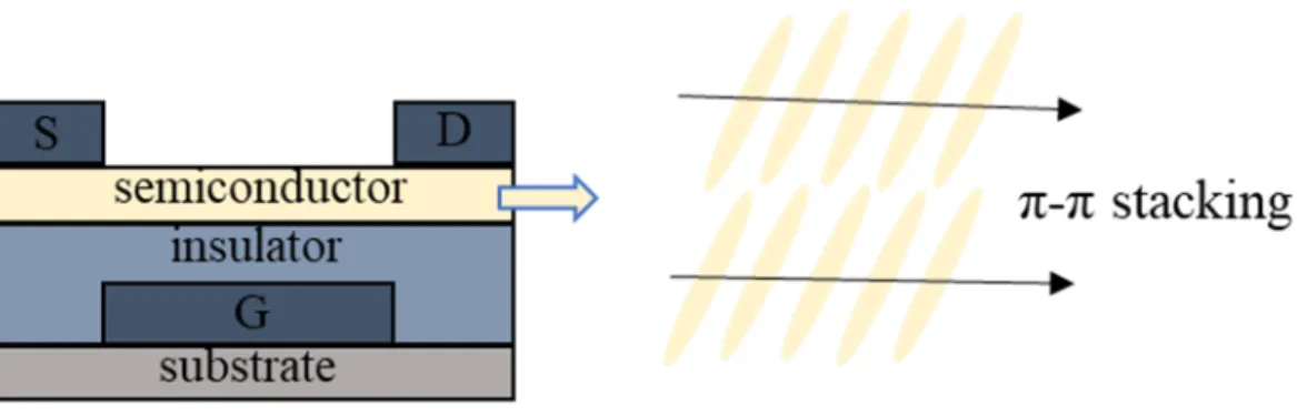
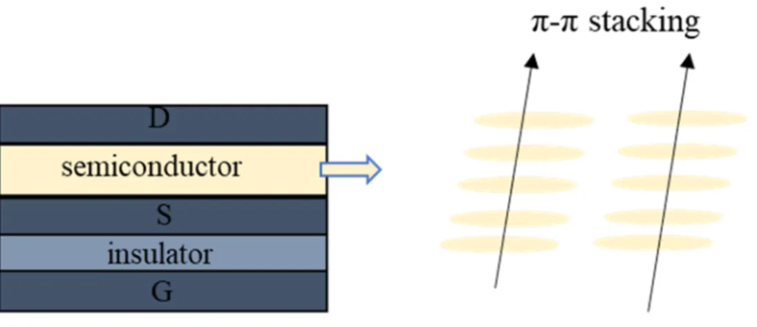
High crystalline structure of organic thin films are required for OFETs in order to obtain high charge carrier mobility. It is possible to achieve the high carrier mobility device since the charge transport direction is directly linking to the molecular orientation; for example, the standing up molecular orientation and lying down molecular orientation in the system of the active layer. In the molecular layers with standing up molecular orientation; that is, π-π stacking direction is parallel to the substrate, in this case, device structure in Figure 1.5 could be con- sidered as suitable device structure because charge transportation direction meets the π-π stack- ing direction. The lying down molecular orientation, i.e, π-π stacking direction is nearly normal or perpendicular to the substrate, in this case, different configurations as in Figure 1.6 is re- quired to meet high carrier mobility in charge transportation process.[90]
Figure 1.5 Structure of conventional OFET with lateral π-π stacking direction of molecules in organic semiconductor layer.
12
Figure 1.6 Structure of vertical-structure OFET (VOFET) with vertical π-π stacking direction of molecules in organic semiconductor layer.
1.3 Importance of the growth control to enhance the performance
The growth of organic semiconductors; single crystal growth to molecular thin film growth have been widely studied because of their application in organic electronics.[91] The performance of the organic devices mainly depend on charge carrier transport in molecular layers. The charge carrier transport from one molecule to another along p-molecular orbital and related to the electron cloud splitting with its nearest molecules. The overlapping degree of neighboring molecular orbital within packing structure determine the charge carrier transport in organic semiconductor which turn linking to the electrical properties.[92] In semiconductor, the electrical conductivity is the transport of the electric current density. The drift current den- sity Jdrift is proportional to the carrier drift velocity, carrier concentration and charge carrier. It can be written as follows;
Jndrift= -q n vdn = q n µnE (1.1)
Jpdrift= q p vdp = q p µpE, (1.2)
13
where, drift velocity for electrons vdn = − µnE, [93] and drift velocity for holes vdp = µpE n = carrier concentration of electrons, p = carrier concentration of holes, q = electric charge carrier.
The total drift current density can be expressed as
Jdrift = Jndrift+ Jpdrift = q (n µn+ p µp) E (1.3)
According to Ohm’s Law, J = σ E = E/ρ , where, σ = conductivity and ρ = resistivity For n-type semiconductor, ρn ≈q n µ1
n
(1.4)
For p-type semiconductor, ρp ≈q p µ1
p
(1.5)
The diffusion length of the carrier can be expressed as,
LD = µn τn E, (1.6)
LD = µp τp E (1.7)
Where, µn and µp are the hole and electron drift mobility, τn and τp are trapping lifetime of the electrons and holes, and E is the electric field.
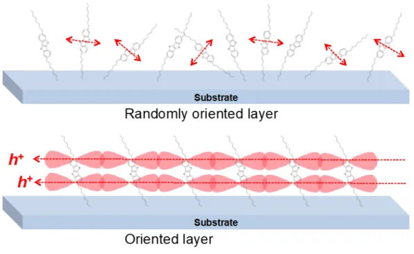
The charge transport properties of a deposited semiconductor layer can be determined by the charge carrier mobility so that the charge carrier mobility is the key of the determining factor for the performance of the organic based electronic devices. The charge carrier diffusion and mobility of organic semiconductor strongly depends on the prepared layer structure and orientation including grain structure of the deposited layer.[90] And randomly orientated and oriented molecular structure (Figure 1.7) are also determining the charge transfer processes in layers. The randomly orientated layer with disordered layer could reduce the carrier diffusion length. The higher crystalline order with oriented layer favored to improve the exciton diffusion length which is leading to the high performance film. [94]
14
Figure 1.7 Schematic illustration of organic layer structure (a) randomly oriented (b) oriented layer on substrate.
A large charge carrier mobility is demanded for all electronic applications. It is specu- lated that the mobility of the organic semiconductor mainly relies on the transfer integral and reorganization energy and both of these are very important parameters in molecular packing structure.[95,96] The transfer integral is the splitting of the highest occupied molecular orbital (HOMO) and the lowest unoccupied molecular orbital (LUMO) which define the distance be- tween π-overlapping distances with neighboring molecules. The reorganization energy is the energy loss when a charge carrier passes through a molecule and is dependent on the conjuga- tion length, degree, and packing of the organic molecules. It is believed that the large transfer integral and low reorganization energy turn out to be high carrier mobility.[97–100] Hence, these two parameters which in turn depend on the molecular packing structure of the organic semiconductors.
15
In general, it is well known that four different kinds of molecular packing structure;
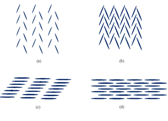
Herringbone stacking without 𝜋-𝜋 overlapping between adjacent molecules, Herringbone stacking with 𝜋-𝜋 overlapping between adjacent molecules, Lamellar 1D-𝜋-stacking and La- mellar 2D-𝜋-stacking which are shown in Figure 1.8.[5][101] Most of studies in molecular based device performance have proven that the molecular packing structure is a key role in charge transport process. In addition to packing structure, crystallinity, orientation, grain struc- ture and morphology are also the factors influencing the performance.[102–104]
Figure 1.8 Four typical packing structure of conjugated molecules (a) Herringbone stacking without 𝜋-𝜋 overlapping between adjacent molecules (b) Herringbone stacking with 𝜋-𝜋 over- lapping between adjacent molecules (c) Lamellar 1D-𝜋-stacking (d) Lamellar 2D-𝜋-stacking.
16
It has been speculated that internal ordering of the organic layers structure could en- hance the charge carrier mobility. The performance of the device efficiency could be improved by controlling the structure of semiconducting layers. In order to deposit the ordered semicon- ducting molecular layers, many techniques have been used including solution deposition, or- ganic molecular beam epitaxy (OMBE) and vacuum deposition and so on.[104–107] It has been proved that the quality of the films depends not only on the preparation techniques but also affected by the parameters like choice of substrate materials, deposition rate, layer thickness, substrate temperature during deposition process. Moreover, surface tuning method as self-as- sembled monolayer (SAM) which is the first prior to deposition of organic semiconductor lay- ers have been able to improve the order of the molecular structure and morphology.[108]
The charge carrier transport as electrical properties and light absorption as optical prop- erties of films depend mainly on the molecular packing and orientation. It has been reported that the orientation of the α,ω-dihexyl-sexithiophene (DH6T) and α-sexithiophene (6T) could be controlled by using Ag(111) substrate, in such case, long axis of molecules are almost nor- mal to the substrate (upright standing) or lying down on the substrate.[109] One of the structure controlling could be done by substrate materials and the manipulating the interface between molecule and substrate materials. The π-conjugated based organic thin films exhibit anisotropic properties so that the molecular orientation could be tuned.
Therefore, controlling the growth of the prepared layers and characterization of the de- posited layers together with understanding of the structure including preferred orientation, grain structure and morphology of the deposited organic layers support the information of how to design and fabricate for quality controlled high-performance electronic devices.
17
1.4 Growth of inorganic and organic thin films and preparation techniques for organic layers
1.4.1 General concepts of thin film growth
Thin film growth are very important for many applications including coating and semi- conductor devices. The physical mechanism of adsorption, surface diffusion, chemical binding and atomic processes at surface and interface were in the process of the thin film growth. And, deposition parameters as deposition rate, and substrate temperature effect the growth of thin films. Generally, thin films were deposited on substrate material, and there are two modes of growth which depend on how the relation occur between the substrate and films, homoepitaxial growth in which crystallographic relation between the substrate and film are under epitaxial, heteroepitaxial growth in which the relation between the substrate material and films are not identical. Thin film growth is controlled by thermodynamics and kinetics. Three scenarios have been described based on the growth modes depending on the interaction between surface and interface energies. There are three different growth modes Frank-van der Merwe (layer-by- layer), Volmer-Weber (islands), Stranski-Krastanov (layer plus islands) according to the sur- face energies such as the substrate surface (gs), the film surface (gf), and the surface-film inter- face (gi). The growth modes are shown in Figure 1.9. [110,111]
The layer-by-layer growth is the 2D growth which is the one monolayer tends to be completely covered before the next layer formed. The continuous layers with less number of defects formed in 2D growth mode. The 2D layer-by-layer growth could be achieved for epitaxial growth,i.e, lattice-matched materials. The Volmer-Weber growth or islands growth is the formation of three dimensional islands. In this mode, atoms or molecules are strongly bound to each other than to the substrate which leads to the 3D islands. In the Stranski- Krastanov growth mode, islands are formed after forming the first few layers. In this growth mode, a transition of growth modes 2D layer-by-layer growth to 3D islands growth happens.
18
The Volmer-Weber and Stranski-Krastanov growth modes tend to form the formation of amorphous or polycrystalline structrue.
Figure 1.9 Schematic illustration of the growth modes: (a) Frank-van der Merwe (layer-by- layer), (b) Volmer-Weber (islands), (c) Stranski-Krastanov (layer plus islands).
Heteroepitaxial growth is crucial for fabricating semiconductor devices. The lattice relation between the deposited film and substrate determine the quality of the films. For example, inorganic thin film of ZnO were prepared on Au(111) and the lattice mismatch between film and substrate is (1x1)ZnO(0001)[1120]//(1x1)Au(111)[110] 12.7%. This film showed randomly oriented ZnO layer with poor performance. The quality of the thin film could
19
be improved by controlling the substrate with lattice matching. The ZnO film prepared on Ga:ZnO film with the lattice relation of (1x1)ZnO(0001)[1120]//Ga:ZnO(0001)[1120] in mismatch 0.8%. That improved ZnO films showed the (0001) oriented ZnO with good performance.[112] Hence, the interface between the film and substrate material in order to get the good quality film could be controlled by substate materials.
1.4.2 Preparation techniques for organic semiconductors and organic thin film growth Organic semiconductors have different kind of properties and it has been used in wide range of applications; conductive coatings, flexible light sources and displays, low-cost printed integrated circuits, and plastic solar cells. Generally, organic semiconductors can be divided into two major classes: conjugated polymers and conjugated low-molecular weight materials (small-organic molecules). Since chemical properties of these materials are different, two major processing methods were performed in order to form organic thin films; solution-processed deposition and dry-processed deposition.
Polymeric macro-molecules are composed of repetition of monomer, and they are sol- uble in organic solvents so that they can be deposited by solution process. For example, the alkyl-substituted polythiophenes, poly(3-hexylthiophene) (P3HT) is a type of highly soluble polymer in a various kind of organic solvents [28] and those kinds of soluble polymers have been prepared by solution process (also called wet processing) such as spin-coating, dip-coating, drop coating, screen printing, inkjet-printing and so on.
There are two sub-group of small-organic molecular materials; pigments which are in- soluble in organic solvents, and dyes which are soluble. In the case of deposition of small or- ganic molecules, since most of small-organic molecules are insoluble in organic solvent, they are deposited by dry processes as thermal vacuum evaporation or thermal sublimation in vac- uum. The promising materials and widely studied of small-organic molecules are pentacene,
20
sexithiophene and copper phthalocyanine. Whatever, it is still challenging the controlled growth of organic semiconductor layers by using solution process or vacuum process.
Organic Thin Film Growth
Organic thin film growth exhibit different growth behaviors as compared to the inor- ganic thin film growth. Inorganic semiconductors are composed of covalent bonding between neighboring atoms while organic semiconductors are established by weak van der Waals forces between molecules. Hlawacek et.al demonstrated that the additional effects of organic thin film growths which are not observed in atomic inorganic growth. [113]
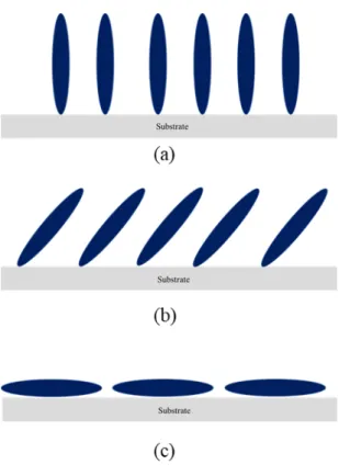
Organic molecules are anisotropic objects and which have internal degrees of freedom including the orientational degree of freedom and the vibrational degree of freedom. The ori- entational degree of freedom (Figure 1.10) which is a new phenomenon because the orientation of molecule may change during the growth, for instance, the long axis of molecules almost upright position on the substrate, and the long axis of molecules almost lying down position.
One of the difference between inorganic and organic thin film growth is that this qualitative phenomenon of orientational degree of freedom are not included in metal or inorganic thin film growth. The vibrational degree of freedom effect to the diffusion behavior of molecules on the substrate surface, and the interaction between substrate and deposited layer.[114]
Another point of difference between organic thin film growth and inorganic film growth is that interaction potential. The interaction between molecules, in such case, van der waal interaction in molecule-molecule, and atomic absorption between substrate-molecule interac- tion which are different. A close lattice matching is required for conventional inorganic semi- conductor thin films growth due to avoid the high density of misfit dislocations. Contradictory
21
to inorganic growth system, it has been found that the crystalline order can be achieved in or- ganic growth system even though the molecule and substrate materials mismatch are highly different.
Figure 1.10 Schematic illustration of organic thin film growth (a) upright position (b) almost standing position with the orientational degrees of freedom (b) lying down position on the sub- strate.
The size differences between unit cells of the molecules and substrates which can cause the low-symmetry structure with multiple domains.[111] The surface of the substrate with dan- gling bonds limited the diffusion and this may lead to disorder film formations because the molecules may dissociate.
22
1.5 Organic Semiconductor Materials investigated in this work
In this thesis, we examined the growth and characteristics of the vacuum-evaporated donor and acceptor type organic molecules of 2,7-dioctyl[1]benzothieno[3,2-b][1] benzothio- phene (C8-BTBT) and N,N'-dioctyl-3,4,9,10-perylenedicarboximide (PTCDI-C8) on single crystal substrates. Both of these molecules compose of conjugated core and alkyl side chains.
Donor type: 2,7-dioctyl[1]benzothieno[3,2-b][1] benzothiophene (C8-BTBT) Acceptor type: N,N'-dioctyl-3,4,9,10-perylenedicarboximide (PTCDI-C8)
The choice of C8-BTBT and PTCDI-C8 molecules is motivated by the reason of they are promising materials to be used in optoelectronics devices and high carrier mobility values have been obtained. The chemical structure of C8-BTBT and PTCDI-C8 are shown in Figure 1.11.
Figure 1.11 The chemical structures of small conjugated molecules (a) 2,7-dioctyl[1]ben- zothieno[3,2-b][1]benzothiophene (C8-BTBT), and (b) N,N'-dioctyl-3,4,9,10-perylenedicar- boximide (PTCDI-C8).
23
2,7-dioctyl[1]benzothieno[3,2-b][1] benzothiophene (C8-BTBT)
2,7-dioctyl[1]benzothieno[3,2-b][1] benzothiophene is a member of BTBT derivatives and it is one of the promising materials to be used in electronic devices. The empirical formula C30 H40 S2 with a formula weight 464.77 g/mol and the melting point is at 108-112 °C. This molecule consists of a one BTBT core and two alkyl chains with a lamella-like alternating structure which is shown in Figure 1.12. It is monoclinic lattice structure with a space group of P21/a.[115] The crystallographic unit cells of C8-BTBT are shown in Table 1.2.
Table 1.2 Crystallographic unit cells of C8-BTBT
a (nm) b (nm) c (nm) α (deg) β (deg) γ (deg)
C8-BTBT 0.5927 0.788 2.918 90 92.443 90
Figure 1.12 Molecular packing structure of 2,7-dioctyl[1]benzothieno[3,2-b][1]benzothio- phene (C8-BTBT), (a) ball and stick structure, (b) space filling structure.
24
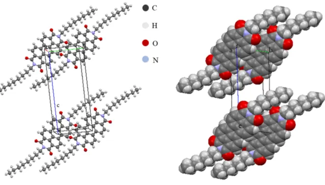
N, N'-dioctyl-3,4,9,10-perylenedicarboximide (PTCDI-C8)
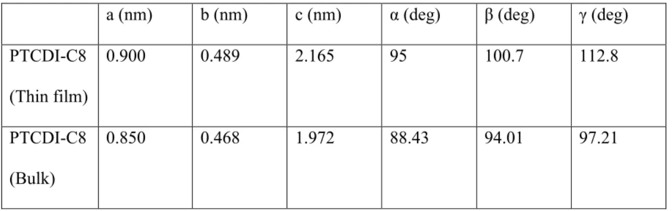
N,N'-dioctyl-3,4,9,10-perylenedicarboximide (PTCDI-C8) is one of the perylene deriv- atives and has been used in active layer of electronic and optoelectronic applications. The chem- ical formula is C40 H42 N2 O4 with a molecular weight of 614.77 g/mol and the melting point is above 300 °C. This molecule is composed of a perylene core and two alkyl side chains with herringbone crystal structure. A schematic diagram of PTCDI-C8 is shown in Figure 1.13. It belongs to triclinic lattice structure with space group P1. The crystallographic structure of PTCDI-C8 has been characterized by A. L. Briseno et.al.[116,117] The structure of PTCDI-C8 parameter slightly altered according to the phase of thin film or bulk. The crystallographic data of both types are given in Table 1.3.
Table 1.3 Crystallographic unit cells of PTCDI-C8 thin film and bulk structure
a (nm) b (nm) c (nm) α (deg) β (deg) γ (deg) PTCDI-C8
(Thin film)
0.900 0.489 2.165 95 100.7 112.8
PTCDI-C8 (Bulk)
0.850 0.468 1.972 88.43 94.01 97.21
25
Figure 1.13 Molecular packing structure of N,N'-dioctyl-3,4,9,10-perylenedicarboximide (PTCDI-C8), (a) ball and stick structure, (b) space filling structure.
26
1.6 Growth of organic molecules C8-BTBT and PTCDI-C8
This work mainly focuses on the fabrication and growth of conjugated small-organic molecular based materials by vacuum thermal evaporation technique. Vacuum thermal evapo- ration can be used to deposit the small-organic semiconductor materials which are insoluble in organic solvents. Figure 1.14 shows the vacuum evaporation system used in this work.
Figure 1.14 Vacuum Thermal Evaporation System
Vacuum evaporation take place inside the bell jar and are equipped with a turbo-molec- ular pump and oil free scroll pump for evacuation process. The filament which acts as heating up for the source materials, and crucible, sensor head and substrate holder are installed inside the vacuum chamber. Water cooling pipes are equipped to the chamber externally. For con- trolling the evaporation process of thickness and deposition rate during deposition, the quartz
27
crystal microbalance sensor is equipped between the crucible and shutter and connect with con- troller. When the current applied to source materials through filament under vacuum, the evap- orated materials is deposited on the substrate which is placing upside down position on the substrate holder. Vacuum thermal evaporation technique offers to control the formation of thin film by the deposition parameters; such as deposition rate, substrate temperature, and layer thickness. The vacuum evaporation technique is capable of precise control of the film thickness and producing the multilayer thin films.
The surface state of the deposited layers is strongly influenced by the thin-film growth, including the choice of the substrate materials and substrate temperature, flux density and the rate of the deposited materials and so on. The growth of organic thin film directly influences the properties of organic semiconductors such as absorption, charge carrier mobility and energy levels, etc. High charge carrier mobility have been obtained by controlling the organic thin film growth, and minimize the defect concentration and grain boundaries. Since film structure in- cluding molecular ordering, orientation, morphology, roughness and defect densities are con- sequence of the growth, manipulation and engineering of the film growth become indispensable.
And, it is also needed to understand the mechanisms for the growth of organic films to optimize the film structure. The kinetic and thermal properties of molecules during deposition process, the driving forces, interaction between surface and interfaces, etc., and these factors impact the growth and nucleation of deposited molecules.
28
1.7 Design of the growth of the C8-BTBT and PTCDI-C8
In this thesis, C8-BTBT and PTCDI-C8 have been used as an organic semiconducting materials and it is required to understand the growth and structure of these organic molecules by vacuum thermal evaporation on single crystal substrates. In the growth of molecular thin films, the orientation of the molecules in single layer, bi-layer and multilayers with respect to substrate depends mainly on the molecule-substrate interaction or molecule-molecule intermo- lecular interaction. The role of substrate type strongly influence on the interface between sub- strate-molecule, and on the growth of organic layers. Therefore, characterization of the layer structure of the organic semiconductor with respect to substrate material and understanding of the molecular packing structure in prepared layers are important role to determine the optical properties as light absorption, and electrical properties as charge carrier transport. It is also evidence that deposition parameters effect the growth of organic semiconductors.
In this study, we designed the heteroepitaxial growth of π-conjugated organic semicon- ductors on quartz glass, (1120) A-, (0001) C-, and (1102) R-single crystal Al2O3 (sapphire), and (100)-, and (111)-single crystal MgO substrates by vacuum thermal evaporation. These layers were deposited with different layer thickness and different substrate temperature. The influence of substrate materials, layer thickness and substrate temperature has been investigated for struc- tural properties, optical properties of light absorption and electrical properties of the deposited organic layers. Understanding the structure and controlling the grain structure of deposited mol- ecules on substrates could be an effective way to progress in organic electronic devices.
29
1.8 Research objectives
Our research work is focusing on heteroepitaxial growth of organic layers on single crystal substrates which are of interest as this structures and configurations are applied in or- ganic based electronic devices. The development of organic electronics mainly depends on the optical and electrical properties of the prepared organic layers. Low crystallinity and random orientation of the prepared layer limit the carrier mobility. On the other hand, organic based devices require highly ordered structure of crystalline properties with preferred orientation. The choice of substrate type has made possible to control the structure and morphology of the or- ganic layers. And also, deposition parameters as layer thickness and substrate temperature were also possible to control the structure of layers including morphology, grain structure and surface roughness. Therefore, characterization of the growth and structure of the organic layers is cru- cial for performance of devices. Several information including the following points are required for the field of organic based applications.
• To investigate the structure and morphology of heteroepitaxial growth of organic sem- iconductor molecule C8-BTBT on inorganic single crystal aluminum oxide and magne- sium oxide substrates with various orientations.
• To investigate the structural, morphological, optical and electrical properties of C8- BTBT organic layer on single crystal C-sapphire substrate with the effect of layer thick- ness and substrate temperature.
• To investigate the growth, structure and optical characteristics of vacuum evaporated PTCDI-C8 layer on single crystal substrates of A-, C-, R- sapphire, and (111)-MgO, and (100) MgO substrates.
30
• To investigate the surface state and morphology of the bi-layer structure of C8-BTBT and PTCDI-C8 by different stacking sequences.
The overall objective of this thesis is to investigate and control of interfaces between organic–organic and organic-single crystal substrate in order to improve the performance of organic devices.
31
1.9 Outline of this study
In this thesis, we study the growth of p-conjugated organic molecules 2,7- dioctyl[1]
benzothieno[3,2-b]benzothiophene (C8-BTBT) and N,N’-dioctyl-3,4,9,10-perylenedicar- boximide (PTCDI-C8) deposited on single crystal sapphire and MgO substrates. The designing of the molecular layers with preferred orientation has been prepared by using vacuum thermal evaporation technique. The dependence of optical and electrical properties on the structure and morphology of organic molecular layers were demonstrated. Moreover, the effect of layer thick- ness and substrate temperature variation on the structure and morphology of deposited molec- ular layers were described. The structure of the organic layer strongly impacts on the optical and electrical properties of the devices. Since the molecular based electronic devices perfor- mance is mainly rely on the deposited organic layers, understanding the formation of layer, i.e structure, which optimize the future progress of the technology of electronic and optoelectronic molecular based devices.
Chapter two gives the growth of p-type organic semiconductor 2,7-dioctyl[1]ben- zothieno[3,2-b]benzothiophene (C8-BTBT) on quartz glass, (1120) A-, (0001) C-, and (1102) R-single crystal Al2O3 (sapphire), and (100)-, and (111)-single crystal MgO substrates by vac- uum thermal evaporation. The morphology and structure of C8-BTBT layers on single crystal substrates with various orientations were investigated by atomic force microscopy (AFM) ob- servations and X-ray diffraction (XRD) analysis. The growth of C8-BTBT on single crystal substrates shows that molecule-molecule interaction is stronger than the molecule-substrate in- teraction according to p-p-stacking-induced molecular ordering with (001) out-of-plane orien- tation development regardless of substrate material and orientation.
In chapter three, organic semiconductor 2,7-dioctyl[1]benzothieno[3,2-b] benzothio- phene (C8-BTBT) were deposited only on a single crystal (0001)Al2O3 (C-sapphire) by vacuum thermal evaporation. The effects of layer thickness and preparation temperature on structural,
32
morphological, optical and electrical characteristics were investigated by X-ray diffraction analysis, atomic force microscopy observation, optical absorption measurement, and resistivity measurement with and without light irradiation. C8-BTBT layers on C-sapphire substrate show (001) out-of-plane orientation irrespective of the preparation conditions; layer thickness and substrate temperature. The C8-BTBT layer was formed by the growth of (001)-C8-BTBT is- lands in direction parallel to the substrate surface and then the growth in direction normal to the substrate surface after the formation of the continuous layer.
In chapter four, the growth of vacuum evaporated N,N'-dioctyl-3,4,9,10-perylenedi- carboximide (PTCDI-C8) layers on single crystal Al2O3 and MgO substrates with various ori- entations were investigated by X-ray diffraction analysis and atomic force microscopic obser- vation. The optical band gap energy was estimated from optical absorption spectra. The growth of the PTCDI-C8 was governed by the π-π stacking like the C8-BTBT growth.
Chapter five presents the fabrication of bi-layer structure with different stacking se- quence of 2,7-dioctyl[1]benzothieno[3,2-b][1]benzothiophene (C8-BTBT) and (001)-N,N' di- octyl-3,4,9,10-perylenedicarboximide (PTCDI-C8) on (0001) Al2O3 (C-sapphire) substrate by vacuum thermal evaporation. The orientation, morphology and surface state of vacuum evapo- rated bi-layers of C8-BTBT and PTCDI-C8 on C-sapphire substrate were investigated by X- ray diffraction and scanning probe microscopy (SPM). The stacking sequence strongly affected to the morphology and surface potential of the bi-layer C8-BTBT and PTCDI-C8 layers.
Finally, chapter six gives a short summary of the results observed from our experiments.
33
REFERENCES
[1] F.M. Li, A. Nathan, Y. Wu, and B. S. Ong, Organic Thin film Transistor Integration: A Hybrid Approach, First Edition, Wiley-VCH Verlag GmbH and Co.KGa A. 1-12 (2011).
[2] M.O. Neill, S.M. Kelly, Ordered Materials for Organic Electronics and Photonics, Adv.
Mater., 23, 566 (2011).
[3] K. Asadi, M. Li, P.W.M. Blom, M. Kemerink, D.M. De Leeuw, Organic ferroelectric opto-electronic memories, Mater. Today., 14, 592 (2011).
[4] Y. Lin, X. Zhan, Small molecule semiconductors for high-efficiency organic photovoltaics, Chem. Soc. Rev., 41, 4245 (2012).
[5] C. Wang, H. Dong, W. Hu, Y. Liu, D. Zhu, Semiconducting π-Conjugated Systems in Field-Effect Transistors:a material odyssey of organic electronics, Chem. Rev., 112, 2208 (2012).
[6] H. Derivatives, J. Louis, A.G. Macdiarmid, Synthesis of Electrically Conducting Organic Polymers : Halogen Derivatives of Polyacetylene, (CH)x, J Chem Soc Chem Comm, 474, 578 (1977).
[7] Y.M. Yang, W. Chen, L. Dou, W. Chang, H. Duan, B. Bob, G. Li, Y. Yang, High- performance multiple-donor bulk heterojunction solar cells, Nat. Photonics, 9, 190 (2015).
[8] H. Nothofer, U. Scherf, M. Gross, D.C. Mu, K. Meerholz, D. Neher, C. Bra, È.P. Chemie, Improving the performance of doped p -conjugated polymers for use in organic light- emitting diodes, Nature, 405, 661 (2000).
[9] P.F. Baude, D.A. Ender, M.A. Haase, T.W. Kelley, D. V Muyres, S.D. Theiss, P.F.
Baude, D.A. Ender, M.A. Haase, T.W. Kelley, D. V Muyres, S.D. Theiss, Pentacene- based radio-frequency identification circuitry Pentacene-based radio-frequency identification circuitry, Appl. Phys. Lett., 3964, 10 (2006).
34
[10] S.J. Bardeen, W. Shockley, Organic thin film transistors, Mater. Today., 7, 20 (2004).
[11] A.N. Sokolov, M.E. Roberts, Z. Bao, Fabrication of low-cost electronic biosensors sensors capable of operating in biologically relevant media, Mater. Today., 12, 12 (2009).
[12] L. Zang, Y. Che, and J.S. Moore, One-Dimensional Self-Assembly of Planar π- Conjugated Molecules : Adaptable Building Blocks for Organic Nanodevices, Acc.
Chem. Res., 41, 1596 (2008).
[13] B. Mukherjee, K. Sim, T.J. Shin, J. Lee, M. Mukherjee, M. Ree, S. Pyo, Organic phototransistors based on solution grown, ordered single crystalline arrays of a π- conjugated molecule, J. Mater. Chem., 22, 3192 (2012).
[14] S. Gunes, H. Neugebauer, and N.S. Sariciftci, Conjugated Polymer-Based Organic Solar Cells, Chem. Rev., 107, 1324 (2007).
[15] B. Mukherjee, Large photoresponse from a small molecule: Application in photodetector and pseudo-transistor, Optik (Stuttg)., 126, 1258 (2015).
[16] C.W.Tang, and S. A. VanSlyke, Organic electrolumescent diodes, Appl. Phys. Lett. 51, 913 (1987).
[17] H. Hoppe, and N.S. Sariciftci, Organic solar cells: An overview, J. Mater. Res. 19, 1924 (2004).
[18] A. Mishra, and P. Bäuerle, Small Molecule Organic Semiconductors on the Move : Promises for Future Solar Energy Technology, Angew. Chem. Int. Ed. 51, 2020 (2012).
[19] C.D. Dimitrakopoulos, and D.J. Mascaro, Organic thin-film transistors: A review of recent advances, IBM J. Reasearch Dev. 45, 11 (2001).
[20] W. Kowalsky, E. Becker, T. Benstem, H.H. Johannes, D. Metzdorf, H. Neuner, and J.
Schöbel, Organic semiconductors: fundamentals and applications, Adv. Solid State Phys.
40, 795 (2000).
35
[21] O. Abanoz, C. Dimitrakopoulos, Recent advances in organic field effect transistors, Turk J Phys. 38, 497 (2014).
[22] C.D. Dimitrakopoulos, P.R.L. Malenfant, Organic thin film transistors for large area electronics, Adv. Mater. 14, 99 (2002).
[23] G.H. Heilmeier, and L.A. Zanoni, Surface studies of α-copper phthalocyanine films, J.
Phys. Chem. Solids, 25, 603 (1964).
[24] F. Ebisawa, J. Kurokawa, S. Nara, J. Appl. Phys. 54, 3255 (1983).
[25] K. Kudo, Field Effect Measurement of Organic Dye Films, Jpn. J. Appl. Phys. 23, 230 (1984).
[26] A. Tsumura, H. Koezuka, T. Ando, Macromolecular electronic device : Fieldeffect transistor with a polythiophene thin film, Appl. Phys. Lett. 49, 1210 (2013).
[27] J.H. Burroughes, C.A. Jones, and R.H. Friend, New semiconductor device physics in polymer diodes and transistors, Nature 335, 137 (1988).
[28] A. Assadi, C. Svensson, M. Willander, O. Inganäs, A. Assadi, C. Svensson, M. Wiilander, O. Inganas, Fieldeffect mobility of poly ( 3hexylthiophene ), Appl. Phys. Lett. 53, 195 (2013).
[29] C. Clarisse, M. T. Riou, M. Gauneau, M. Le Contellec, Field-effect transistor with diphthalocyanine thin film, M. Elect. Lett. 24, 674 (1988).
[30] J. Paloheimo, E. Punkka, H. Stubb, P. Kuivalainen, in Lower Dimensional Systems and Molecular Devices, Proceedings of NATO ASI, Spetses, Greece, Plenum, New York 1989.
[31] G. Horowitz, D. Fichou, X. Peng, Z. Xu, F. Garnier, M. Molrculaires, H. Dunant, R.
March, M. Balkanski, A Field-effect transistor based on conjugated alpha-sexithienyl, Solid State Commun. 72, 381 (1989).
36
[32] G. Horowitz, X. Peng, D. Fichou, F. Garnier, Role of the semiconductor/insulator interface in the characteristics of π-conjugated-oligomer-based thin-film transistors, Synth. Met. 51, 419 (1992).
[33] F. Garnier, A. Yassar, R. Hajlaoui, F. Deloffre, P. Alnott, Molecular Engineering of Organic Semiconductors: Design of Self-Assembly Properties in Conjugated Thiophene Oligomers, P. J. Am. Chem. Soc. 115, 8716 (1993).
[34] H. Fuchigami, A. Tsumura, H. Koezuka, Polythienylenevinylene thinfilm transistor with high carrier mobility, Appl. Phys. Lett. 63, 1372 (1993).
[35] F. Garnier, R. Hajlaoui, A. Yassar, P. Srivastava, All-Polymer Field-Effect Transistor Realized by Printing Techniques,P. Science 265, 1684 (1994).
[36] A. Dodabalapur, L. Torsi, H.E. Katz, Organic Transistors : Two-Dimensional Transport and Improved Electrical Characteristics, Science 268, 270 (1995).
[37] C.D. Dimitrakopoulos, A.R. Brown, A. Pomp, C.D. Dimitrakopoulos, A.R. Brown, A.
Pomp, Molecular beam deposited thin films of pentacene for organic field effect transistor applications Molecular beam deposited thin films of pentacene for organic field effect transistor applications, J. Appl. Phys. 80, 2501 (1996).
[38] Z. Bao, A.J. Lovinger, A. Dodabalapur, Z. Bao, A.J. Lovinger, A. Dodabalapur, Organic fieldeffect transistors with high mobility based on copper phthalocyanine Organic field- effect transistors with high mobility based on copper phthalocyanine, Appl. Phys. Lett.
69, 3066 (1996).
[39] Z. Bao, A. Dodabalapur, A.J. Lovinger, transistor applications with high mobility Soluble and processable regioregular poly ( 3-hexylthiophene ) for thin film field-effect transistor applications with high mobility, J. Appl. Phys. Lett. 69, 4108 (1996).
[40] Y.Y. Lin, D.J. Gundlach, T.N. Jackson, In 54th Annual Device Research Conference Digest, IEEE: Santa Barbara, CA, USA, p.80, (1996).
37
[41] Y.Y. Lin, D.J. Gundlach, S. Nelson, T.N. Jackson, IEEE Electrin Device Lett. 18, 606 (1997).
[42] H. Sirringhaus, R.H. Friend, X.C. Li, S.C. Moratti, A.B. Holmes, Bis ( dithienothiophene ) organic field-effect transistors with a high ON/ OFF ratio, Appl.
Phys. Lett. 71, 3871 (1997).
[43] C.D. Dimitrakopoulos, A. Afzali-ardakani, B. Furman, J. Kymissis, S. Purushothaman, Trans- trans- 2,5- Bis- [2- {5- (2,2'-bithienyl)} ethenyl] thiophene : synthesis, characterization , thin film deposition and fabrication of organic field-effect transistors, Synthetic Metals, 89 193 (1997).
[44] H. Sirringhaus, N. Tessler, R.H. Friend, Integrated Optoelectronic Devices Based on Conjugated Polymers, Science 280, 1741 (1998).
[45] H.E. Katz, A.J. Lovinger, J.G. Laquindanum, α,ω -Dihexylquaterthiophene: A Second Thin Film Single-Crystal Organic Semiconductor, Chem. Soc.10, 457 (1998).
[46] J.G. Laquindanum, H.E. Katz, A.J. Lovinger, M. Hill, R. V August, Synthesis , Morphology , and Field-Effect Mobility of Anthradithiophenes, J. Am. Chem. Soc. 120, 664 (1998).
[47] H.E. Katz, A.J. Lovinger, J. Johnson, C. Kloc, T. Siegrist, W. Li, Y.Y. Lin, A.
Dodabalapur, A soluble and air-stable organic semiconductor with high electron mobility, Nature 404, 478 (2000).
[48] A. Afzali, C.D. Dimitrakopoulos, T.L. Breen, High-Performance , Solution-Processed Organic Thin Film Transistors from a Novel Pentacene Precursor, J. Am. Chem. Soc.124, 8812 (2002).
[49] P.R. L. Malenfant, C.D. Dimitrakopoulos, J.D.Gelorme, L.L.Kosbar, and T.O. Graham, N-type organic thin-film transistor with high field-effect mobility based on a N,N'- dialkyl-3,4,9,10-perylene tetracarboxylic diimide derivative, Appl. Phys. Letts. 80, 2517
38
(2002).
[50] T.W. Kelley, L.D. Boardman, T.D. Dunbar, D. V Muyres, M.J. Pellerite, T.P. Smith, High-Performance OTFTs Using Surface-Modified Alumina Dielectrics, J. Phys. Chem.
B. 107, 5877 (2003).
[51] R.W.I. De Boer, M.E. Gershenson, A.F. Morpurgo, V. Podzorov, Organic single- crystal field-effect transistors, Phys. Status Solidi A. 201, 1302 (2004).
[52] V.C. Sundar, J. Zaumseil, V. Podzorov, E. Menard, R.L. Willett, T. Someya, M.E.
Gershenson, J.A. Rogers, Elastomeric Transistor Stamps : Reversible Probing of Charge Transport in Organic Crystals, Science 303, 1644 (2004).
[53] N. Stingelin-stutzmann, E. Smits, H. Wondergem, C. Tanase, P. Blom, P. Smith, D.D.E.
Leeuw, solution-processed rubrene hypereutectics, Nat Mater. 4, 601 (2005).
[54] K.Takimiya, H. Ebata, K. Sakamoto, T. Izawa, T. Otsubo, Y. Kunugi, 2,7-
Diphenyl[1]benzothieno[3,2-b]benzothiophene, A New Organic Semiconductor for Air- Stable Organic Field-Effect Transistors with Mobilities up to 2.0 cm2V-1s-1, J. Am.
Chem. Soc.128, 12604 (2006).
[55] S.K. Park, T.N. Jackson, J.E. Anthony, D. A. Mourey, High mobility solution processed 6,13-bis(triiopropyl-silylethynyl)pentacene organic thin film transistors, Appl. Phys.
Lett. 91, 063514 (2007).
[56] O.D. Jurchescu, M. Popinciuc, B.J. Van Wees, T.T.M. Palstra, Interface-Controlled , High-Mobility Organic Transistors, Adv. Mater. 19, 688 (2007).
[57] M. Yamagishi, J. Takeya, Y. Tominari, Y. Nakazawa, T. Kuroda, S. Ikehata, M. Uno, T.
Nishikawa, T. Kawase, High-mobility double-gate organic single-crystal transistors with organic crystal gate insulators, Appl. Phys. Lett. 90, 182117 (2007).
39
[58] Y. Takahashi, T. Hasegawa, S. Horiuchi, R. Kumai, Y. Tokura, G. Saito, High mobility field-effect transistor based on hexamethylenetetrathiafulvalene with organic metal electrodes, Chem. Mater. 19, 6382 (2007).
[59] B.L. Li, Q. Tang, H. Li, X. Yang, W. Hu, Y. Song, Z. Shuai, W. Xu, Y. Liu, D. Zhu, An Ultra Closely π -Stacked Organic Semiconductor for High Performance Field-Effect Transistors, Adv. Mater. 19, 2613 (2007).
[60] S. Haas, Y. Takahashi, K. Takimiya, T. Hasegawa, High-performance dinaphtho- thiophene single crystal field-effect transistors. Appl. Phys. Lett. 95, 022111 (2009).
[61] H. Minemawari, T. Yamada, H. Matsui, J. Tsutsumi, S. Haas, R. Chiba, R. Kumai, T.
Hasegawa, Inkjet printing of single-crystal films, Nature. 475, 364 (2011).
[62] G. Giri, E. Verploegen, S.C.B. Mannsfeld, S. Atahan-Evrenk, D.H. Kim, S.Y. Lee, H.A.
Becerril, A. Asupuru-Guzik, M.G. Toney, Z. Bao, Tuning charge transport in solution- sheared organic semiconductors using lattice strain, Nature 480, 504 (2011).
[63] M.J. Kang, I. Doi, H. Mori, E. Miyazaki, K. Takimiya, M. Ikeda, H. Kuwabaa, ( C n - DNTTs ): Organic Semiconductors for High- Performance Thin-Film Transistors, Adv.
Mater, 23, 1222 (2011).
[64] K. Nakayama, Y. Hirose, J. Soeda, M. Yoshizumi, T. Umemura, M. Uno, W. Li, M.J.Kang, M. Yamagishi, Y. Okada, E. Miyazaki, Y. Nakazawa, A. Nakao, K. Takimiya, J. Takeya, Patternable solution-crystallized organic transistors with high charge carrier mobility, Adv. Mater. 23, 1626 (2011).
[65] A.N. Sokolov, S. Atahan-evrenk, R. Mondal, H.B. Akkerman, A.P. Zoombelt, Z. Bao, A. Aspuru-guzik, From computational discovery to expermental characterization of a high hole mobility organic crystal, Nature Communications 2, 437 (2011).
[66] M. Watanabe, Y.J. Chang, S. W. Liu, T.H. Chao, K. Goto, M.M.Islam, C. H.Yuan, Y.
T.Tao, T. Shinmyozu, T.J. Chow, The synthesis, crystal structure and charge-transport
40
properties of hexacene, Nat. Chem. 4, 574 (2012).
[67] A.Y. Amin, A. Khassanov, K. Reuter, T. Meyer-friedrichsen, M. Halik, Low-voltage organic field effect transistors with a 2-Tridecyl[1] benzothieno[3,2-b][1]
benzothiophene semiconductor layer, J. Am. Chem. Soc. 134, 16548 (2012).
[68] J. Li, Y. Zhao, H.S. Tan, Y. Guo, C.A. Di, G. Yu, Y. Liu, M. Lin, S.H. Lim, Y. Zhou, H.
Su, B.S. Ong, A stable solution-processed polymer semiconductor with record high- mobility for printed transistor, Sci. Rep. 2, 754 (2012).
[69] Y. Diao, B.C. Tee, G. Giri, J. Xu, D.H. Kim, H.A. Becerril, R.M. Stoltenberg, T.H. Lee, G. Xue, S.C.B. Mannsfeld, Z. Bao, Solution coating of large-area organic semiconductor thin films with aligned single-crystalline domains, Nat. Mater. 12, 665 (2013).
[70] N. Kurihara, A. Yao, M. Sunagawa, Y. keda, K. Terai, H. Kondo, M. Saito, H. Ikeda, H.
Nakamura, High-Mobility Organic Thin-Film Transistors Over 10 cm 2 V -1 s -1 Fabricated Using Bis ( benzothieno ) naphthalene Polycrystalline Films, Japanese Journal of Applied Physics 52, 05DC11-1 (2013).
[71] G. Kim, S. Kang, G.K. Dutta, Y. Han, T.J. Shin, Y. Noh, C. Yang, A thienoisoindigo- naphthalene polymer with ultrahigh mobility of 14.4 cm 2 /V s That Substantially Exceeds Benchmark Values for Amorphous Silicon Semiconductors, J. Am. Chem. Soc.
136, 9477 (2014).
[72] S. Y. Yang, K. Shin, C.E. Park, The Effect of Gate-Dielectric Surface Energy on Pentacene Morphology and Organic Field-Effect Transistor Characteristics, Adv. Funct.
Mater 15, 1806 (2005).
[73] A. Swist, J. Soloducho, Organic semiconductors-materials of the future?, Chemik. 66, 293 (2012).
[74] W. Brütting, Physics Organic Semiconductors, Wiley-VCH, (2005).