i
A STUDY ON CODE-MODULATED
SYNCHRONIZED-OOK TRANSCEIVER FOR
LOW POWER WIRELESS SENSOR NETWORKS
NGUYEN VAN TRUNG
A DISSERTATION
PRESENTED TO THE FACULTY
OF THE UNIVERSITY OF ELECTRO-COMMUNICATIONS IN CANDIDACY FOR THE DEGREE
OF DOCTOR OF PHILOSOPHY
RECOMMENDED FOR ACCEPTANCE
BY THE DEPARTMENT OF ENGINEERING SCIENCE SUPERVISOR: KOICHIRO ISHIBASHI & CONG-KHA PHAM
ii
iii
Acknowledgements
First of all, I would like to offer my deepest appreciation to my supervisors, Professor Koichiro Ishibashi and Professor Cong-Kha Pham, for their patient guidance, enthusiastic encouragement and useful critiques during the doctoral course at UEC. Throughout the course, I received not only scientific instruction in my research but also useful advice for coping with problems in my life. Thanks to their supporting, originating with lack experience in scientific research, I became more matured. I hope that in the future we still maintain the good relationship and have more chance to cooperate.
Next, I would also like to extend my thanks to Associate Professor Ryo Ishikawa and Doctor Yasuo Sato for their technical support, to our lab secretaries and staffs of Graduate School of Informatics and Engineering, Department of Engineering and Science for their enthusiastic support to complete official procedures.
I wish to thank the University of Electro-Communications (UEC) and Vietnam Ministry of Education and Training, Vietnam International Education and Development (VIED) for giving me a chance to study in Japan. I also would like to thank the International Student Offices (ISO) staffs and lecturers for their supporting during my course.
I would like to acknowledge JST-CREST Grant Number JPMJCR16Q1, Japan and VLSI Design and Education Center (VDEC), the University of Tokyo in collaboration with Synopsys, Inc. and Cadence Design Systems, Inc. for their supporting for this work.
Relating to my health condition, I would like to express my profound gratitude to doctors and nurses in Tokyo Metropolitan Tama Medical Center Hospital for treating my disease and helping me to be able to continue my research and complete the doctoral course.
Last but not least, I would like to express my gratitude to my teachers and my colleagues in the Faculty of Radio-Electronics, Le Quy Don Technical University, Vietnam for provide the best condition for me to pursue the doctoral course; to all members of ISHIBASHI Lab and PHAM Lab for their kindness and their support; to my friends and seniors who always encouraged me to keep going on the research way. Finally, I would like
iv
to thank and give my love to my parents, my relatives for their encouragement, to my wife and my son who sacrificed too much for me and always with me to complete the doctoral course.
v
Copyright © 2019 Nguyen Van Trung
All right reserved.
vi
vii
Abstract
A Study on Code-Modulated Synchronized-OOK Transceiver for Low
Power Wireless Sensor Networks
NGUYEN VAN TRUNG
Doctoral Program in Electronics Engineering The University of Electro-Communications
Wireless Sensor Networks (WSNs) currently has attracted significant attention because of its unlimited potential. Normally, a WSN composes of few or hundreds or even thousands spatially distributed sensor nodes which are able to sense, self-process and communicate through wireless channel. To satisfy these function, a sensor node often consists of sensor, microprocessor, memory, power supply and RF communication device. In which, transmission and reception using RF transceiver consumes most power of a sensor node. In condition that sensor node is supplied by limited power source, reducing power consumption of RF transceivers is critical to prolong lifetime of sensor node. Besides, along to technology advancement, wireless devices have been used popularly, which leads to a scenario that sensor node operates simultaneously with other nodes and other wireless devices in the vicinity. These easily become interference sources which can have negative effects on WSN. Such fact demands enhancing immunity of RF transceiver in WSNs. This thesis studies to design a low power TRX system high immunity to interference using for low power WSNs.
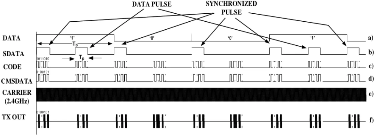
In order to achieve the target, this thesis considers several issues of modulation scheme, operation mode and hardware design. In terms of modulation scheme, the study exploits low power advantage of OOK and S-OOK system in combination with ability of withstanding to interference of spread spectrum technique to propose Code-Modulated Synchronized-OOK (CMS-OOK) scheme. CMS-OOK system not only reduce significantly power consumption but also enhance system immunity to interference by assigning different codes to different nodes. According to this scheme, DATA which needs to be sent, firstly, is
viii
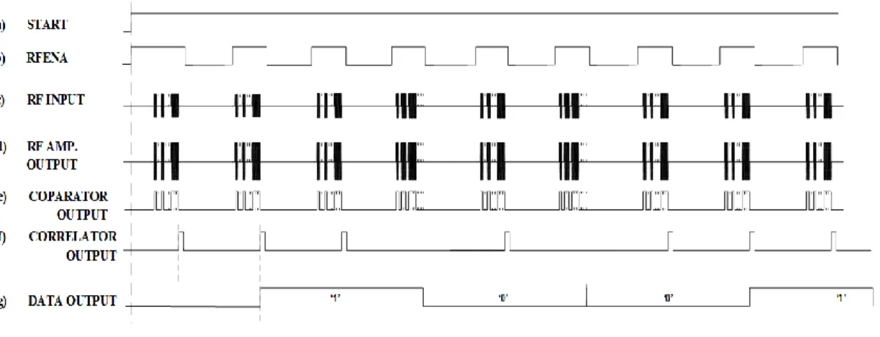
transformed to synchronized data (SDATA) including synchronized pulses and data pulses. By this way, data ‘1’ is represented by a synchronized pulse and a data pulse while only a synchronized pulse is used to display data ‘0’. Then, a code, which is generated in those pulses interval, is multiplied with SDATA to create Code-Modulated Synchronized Data (CMSDATA). Finally, this signal is modulated by 2.4GHz carrier and radiated to free space through antenna. In order to demodulate CMS-OOK signal is sent from the TX, CMS-OOK RX utilizes envelop detector and comparator structure in cooperation with digital correlator. Issue of synchronizing received signal and the pre-agreed code is addressed by using 2x- or 4x-oversampling digital correlator.
Regarding to operation mode, the system deploys intermittent communication or normally-off operation to decrease power consumption. Intermittent and normally-off operation mode are originated as a way of computing which is used for energy saving purpose. Authors who develop Beat sensor networks applied normally-off operation mode to their system and manifested its energy efficiency. Other group implemented their receiver with intermittent operation can reduce a half of power consumption. The challenge of these operation modes is the settling time of carrier oscillator. Whenever sensor node wants to send a data, it takes time to settle the carrier oscillator from sleep (intermittent operation) or power-off (normally-off operation) state. This time is call settling time. During this time, RF TX consumes amount of energy. The longer settling time of TX is, the more power is dissipated. The proposed CMS-OOK TX utilizes low power ring oscillator (RO) as carrier generator, which usually has short settling time. Whereby, TX can be almost completely turned-off (normally-off operation) or consume a small sleeping power (intermittent operation) when no data is sent and wake-up fast from the power-down state or sleep state to start transmitting data. This short wake-up time helps CMS-OOK TX save more power than that of other TXs which use crystal oscillator or PLL oscillator with high stable frequency but long setting time.
Relating to hardware design, the thesis considers about architecture, circuit design and fabrication technology. Firstly, 65nm SOTB CMOS technology is chosen for implementation of CMS-OOK TRX system. With valuable features such as low operation voltage, small leakage current, ability of body bias control, SOTB CMOS commensurate
ix
with low power applications. Besides, the thesis also investigates RF characteristics of SOTB devices. A pair of SOTB NMOS and PMOS with gate length of 60nm, total width of 8x6µm = 48 µm were designed, fabricated and evaluated. Devices evaluation results show cut-off and maximum frequency of NMOS are, respectively, 40GHz and 28GHz, while those of PMOS are consequently 26GHz and 20GHz. These frequencies are far higher than 2.4GHz frequency, the target frequency of the proposed CMS-OOK TRX, which guarantees that these devices are able to use for RF applications.
Basing on SOTB devices, a pair of 2.4GHz TX and RX using CMS-OOK modulation scheme are designed, simulated and fabricated. On TX side, OOK modulation allows to utilize large jitter carrier oscillator like ring oscillator (RO) as well as high-efficiency and low-linearity E-class power amplifier. This contributes on reducing power for TX. Besides, thanks to code modulation and sweeping body bias voltage of SOTB devices, bandwidth of TX output spectrum is widen and peak power of spectrum is reduced. Evaluated results of 65nm SOTB device-based CMS-OOK TX chip show that the TX consumes average 83µW at 1kbps data transmission and achieves -62dBm/MHz power spectral density with 15MHz bandwidth (using 31-bit code), which satisfies the FCC radio regulations. On the other side, we also propose a CMS-OOK RX which, then, is simulated and fabricated on 65nm SOTB CMOS. The RX consists of analog RF front-end including a low noise amplifier (LNA) in series with 4-stage RF amplifier, followed by envelope detector and comparator, and a digital part at the end. LNA and RF amplifier contribute on reducing noise figure and increasing gain to improve RX sensitivity. In digital part, a 2x-oversampling digital correlator is used to decode received CMS-OOK signal in order to recover data clock and data sent from the TX. The digital part also generates a window pulse (RFENA) to turn-on and turn-off RF front-end to save power consumption. By simulation using SOTB CMOS models, analog part of the RX consumes average 38.8µW at 1kbps data rate with -76 dBm sensitivity. Besides, system simulation shows a 10 times lower BER of CMS-OOK system in comparison with that of OOK system in condition that interference is not too strong, which states that immunity of RX is improved. Experiment results of TRX system with discrete TRX RF modules and FPGA board show that CMS-OOK scheme can be implemented successfully.
x
CMS-OOK TRX brings to us a lot of benefits when applied to low power WSNs. Firstly, in term of power consumption, as the wake-up time is very short, the CMS-OOK TX nearly consumes no power during this time. This helps the TX save much power in comparison with other TXs using crystal oscillator or PLL oscillator. For example, in an experiment in our laboratory with a normally-off WSN using LoRa TRX with crystal oscillator shows that the wake-up time takes 150ms and TX consumes average 25mW, this means TX consumes total 3.75mJ which even is much higher than required power to send necessary data (2.5mJ). On the RX side, applying S-OOK technique in combination with code modulation reduces significant power consumption. Saved power is depends on the ratio between data bit duration and synchronized pulse duration. As a result, maintaining power supply for TRX becomes more relaxed, which is suitable to EHWSN with intermittent or normally-off operation. Secondly, Code-Modulation and sweeping body bias voltage in TX are spreading spectrum technique which produces numerous advantages. With wider bandwidth and lower peak power transmission, CMS-OOK TRX easily satisfies the radio regulations. Moreover, spreading-spectrum technique helps TRX increase not only the sensitivity but also the immunity to interference of RX by 4dB in signal to interference ratio (SIR) in comparison with that of OOK TRX. This means communication range and reliability of TRX are enhanced. With these benefits, CMS-OOK TRX can be applied for low power WSNs.
xi
xii
Contents
Acknowledgements ... iii
Abstract... vii
List of Tables ... xv
List of Figures ... xvi
List of Abbreviations ... xix
Chapter 1 ... 1
Introduction ... 1
1.1 Research background ... 1
1.1.1 Wireless sensor networks ... 1
1.1.2 Energy harvesting WSN with intermittent and normally-off operation ... 4
1.1.3 Interference in wireless communication – Radio regulations ... 6
1.2 Purpose of the study ... 7
1.3 Dissertation layout... 10
Chapter 2... 15
Considerations of Wireless Sensor Networks for Low Power, Longer Communication Distance and Immunity to Interference ... 15
2.1 Low power TRX design ... 15
2.1.1 Link budgeting ... 15
2.1.2 Modulation scheme and architecture ... 16
2.1.3 Operation mode ... 18
2.2 Spread-spectrum technique ... 18
2.4 Conclusion ... 22
Chapter 3... 28
xiii
3.1 Synchronized-OOK modulation ... 29
3.2 Spread-Spectrum communications and Direct-Sequence Spread-Spectrum technique ... 31
3.3 Code-Modulated Synchronized-OOK scheme ... 32
3.4 Chapter conclusion ... 37
Chapter 4... 39
Wide bandwidth CMS-OOK Transmitter Using 65nm SOTB CMOS Technology with Sweeping Body Bias Technique ... 39
4.1 Block diagram and operation ... 39
4.2 A 65nm SOTB devices-based TX circuit ... 40
4.3 Simulation results ... 41
4.4 Experiment results ... 45
4.5 Chapter conclusion ... 50
Chapter 5... 52
Low-Power and High Immunity to Interferences CMS-OOK Receiver ... 52
5.1 System architecture of the CMS-OOK RX ... 52
5.2 Circuit level design bases on 65nm SOTB devices ... 53
5.2.1 Analog part ... 53
5.2.2 Digital part... 59
5.3 Simulation results ... 64
5.5 CMS-OOK TRX system experiment with discrete RF module and FPGA board. ... 69
5.6 Conclusion ... 71
Chapter 6... 73
Consideration of Applying CMS-OOK Transceiver to Low Power Wireless Sensor Networks ... 73
6.1 Power consumption of the TX ... 73
6.2 Interference resistance of CMS-OOK TRX system ... 78
6.3 Interference experiment of system using discrete RF modules and FPGA ... 82
xiv Chapter 7... 87 CONCLUSION ... 87 APPENDIX A ... 90 APPENDIX B ... 93 AUTHOR BIOGRAPHY………... 95
xv
List of Tables
1.1 Energy contribution in a sensor node……… 7
2.1 Settling time comparison……… 18
4.1 Comparison with State of Art (TX)………... 50
xvi
List of Figures
1.1 Wireless Sensor Networks 2
1.2 General architecture of a Sensor Node 3
1.3 Power schematic of transmitter in
a) Intermittent operation and b) Normally-off operation
4
1.4 Power consumption comparison between conventional operation and normally-off operation [1-14]
5
1.5 Interferences in the vicinity 6
1.6 Power distribution in the low-energy adaptive clustering hierarchy sensor node
8
2.1 A generic low-complexity TRX system architecture 16
2.2 Power versa sensitivity radio survey 17
2.3 Spread Spectrum Communications system 19
2.4 The structure of SOTB CMOS 20
2.5 Chip photo of investigated SOTB 21
2.6 Measured FT and Fmax of 65nm SOTB CMOS at Vd = 1.2V, Vg = 0.65V,
Vb = 0 for NMOS, Vd = - 1.2V, Vg = -0.65V, Vb = 0 for PMOS
21
3.1 a) Conventional OOK signal b) S-OOK signal 29 3.2 Current consumption of the S-OOK RF front-end 30 3.3 SS communication system (a) and spectrum transformation (b) 31
3.4 Waveform operation of CMS-OOK TX 32
3.5 Waveform operation of S-OOK RX 33
3.6 Architecture of CMS-OOK TX 35
3.7 Architecture of CMS-OOK RX 35
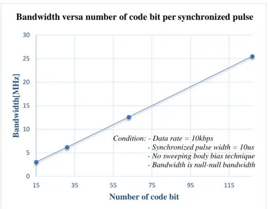
3.8 Dependence of BW on number of code bit during synchronized pulse duration
36
xvii
4.2 Architecture of the digital part 40
4.3 Timing chart of the CMS-OOK TX 40
4.4 Detailed schematic of the analog part of CMS-OOK TX 42 4.5 Waveform of TX produced by HSPICE simulator 43 4.6 Dependence of carrier frequency on body voltage swing (simulated) 43 4.7 Dependence of RO BW AND TX BW on body voltage swing
(simulated)
44 4.8 Dependence of TX output spectrum on body voltage swing (simulated) 44 4.9 Layout picture of TX analog part and TX board 46
4.10 Experiment setting up diagram 46
4.11 Measured real-time waveform (31-bit code) (1) Synchronized pulse, (2) Data pulse
47
4.12 Spectrum of CMS-OOK signal with single carrier frequency 47
4.13 Spectrum of S-OOK and CMS-OOK signals 48
5.1 Spectrum of S-OOK and CMS-OOK signals 52
5.2 CMS-OOK RX in combination with Wake-up RX 54
5.3 Operation waveform of CMS-OOK RX 54
5.4 Detailed schematic of RF front-end (Analog part) 55
5.5 LNA schematic 56
5.6 4-stage RF Amplifier 56
5.7 Envelope detector and Comparator 57
5.8 Spiral inductor 58
5.9 An on-chip 14nH spiral inductor in 65nm SOTB process 58
5.10 Block diagram of digital part 59
5.11 Timing chart of digital part 59
5.12 31-bit 2x-sampling digital correlator 60
5.13 Detailed structure of RFENA Generator and S-OOK demodulator 61 5.14 Schematic (a) and symbol (b) of Pulse Forming, Short Pulse and Long
Pulse blocks
62
5.15 Timing chart for recovering data 62
xviii
5.17 Layout picture of CMS-OOK RX 65
5.18 Transient simulation results 66
5.19 Noise figure, S11 and S21 of RF front-end 67
5.20 Simulation results of digital part 67
5.21 Experiment setting up diagram 69
5.22 Experiment setting up 69
5.23 Operation wave form of experiment 70
6.1 Intermittent operation TX 74
6.2 Normally-off operation TX 74
6.3 Normally-off operation of CMS-OOK TX 74
6.4 Waveform of original data, synchronized data and CMS data 76 6.5 Co-located TX inside same WSN as an interference source 78 6.6 Simulation diagram of system with 2 TX and 1 RX 79 6.7 Adjusting threshold of correlator to recover data 80 6.8 BER comparison between OOK and CMS-OOK TRX 81 6.9 BER comparison between OOK and CMS-OOK TRX at low SNR 81 6.10 Interference experiment of CMS-OOK system with 2 TXs and 1 RX
configuration
83
xix
List of Abbreviations
ADC Analog to Digital Converter
BER Bit Error Rate
BW Band Width
CMOS Complementary Metal Oxide Semiconductor
CMS-OOK Code-Modulated Synchonized-OOK
CS Common Source
DAC Digital to Analog Converter
DS-SS Direct Sequence Spread Spectrum
EH Enery Harvesting
EHWSNs Enery Harvesting Wireless Sensor Networks
FD-SOI Fully Depleted Silicon-On-Insulator
FOM Figure Of Merit
FSK Frequency Shift Keying
IoT Internet of Thing
LNA Low Noise Amplifier
MCU MicroController Unit
OOK On-Off Keying
PLL Phase Locked Loop
PSD Power Spectral Density
PSK Phase Shift Keying
RF Radio Frequency
RO Ring Oscillator
RX Receiver
SN Sensor Node
SER Symbol Error Rate
SIR Signal to Interference Ratio
SNIR Sinal to Noise and Interference Ratio
xx
S-OOK Synchonized-On-Off Keying
SOTB Silicon On Thin Buried Oxide
SS Spread Spectrum
TRX Transceiver
TX Transmitter
ULP Ultra Low Power
UWB Ultra Wide Band
1
Chapter 1
Introduction
In this chapter, the background of Wireless Sensor Networks, energy harvesting Wireless Sensor Networks with intermittent and normally-off operation modes and interference in wireless communication are presented. Then, the purpose of the study is shown through the challenges to achieve study targets. Finally, that is the dissertation layout for clarifying the structure of this dissertation.
1.1 Research background
1.1.1 Wireless sensor networks
Recently, Internet-of-Things (IoTs) has been emerged as one of the most important parts of current technology revolution. It helps to realize communication between a lot of objects, machines and devices [1-1, 1-2]. Wireless Sensor Networks (WSNs) are the key elements of the IoTs because they can help users to interact with their environment by sensing or controlling physical parameters. Collaborating of individual nodes is a good way to fulfill tasks that single node is incapable of doing so. Because of downsides of wire communication such as high cost, less flexibility and mobility and so on, wireless communication is commensurate to enabling this collaboration. Applications of WSNs lie on various sections from environment monitoring, smart home to medical applications and so on. Besides, recent advances in technology have made it possible to produce not only tiny size with multiple sensors but also low power consumption, low cost, adaptability, mobility and convenience. These make the usage of WSNs be increasing exponentially and become an attractive object to many researchers. [1-3, 1-4]
2
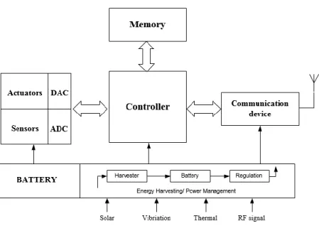
A WSN normally composes of few to several hundreds or even thousands spatially sensor nodes which are capable of sensing, data self-processing and communicating to the others through wireless channel [1-5] as shown in Fig. 1.1. In order to fulfill these functions, a sensor node (SN) often consists of five main components: sensors/actuators, microcontroller, memory, power supply and communication device (Fig. 1.2). In which, microcontroller is the heart of a wireless sensor node because it accumulates information from the sensors, self-processes this data, makes decision of when and where to send the data, receives data from other sensor nodes, and decides react of the actuators. The sensors monitor and collect necessary data from its objective in shape of electrical signals which are led to the controller via Analog to Digital Converter (ADC). The actuators are used to execute commands from the controller corresponding to a particular task such as controlling a motor, a light and so on. In many cases, it is necessary to use memory to store intermediated sensors data, packets from other nodes, and so on. Next component of the sensor node is radio communication device which establishes wireless connections to the other sensor nodes. Normally, it is convenient to use a communication device which combines transmitter (TX) and receiver (RX) as a single entity called transceiver (TRX). All sensor node is powered up by power supply which can be batteries or energy harvesting circuits with limited amount of energy, hence limiting the sensor node lifetime. Popularly, battery can
3
rarely satisfy design goals of long network life time and high reliability while energy harvesting circuits, which convert various kinds of energy to electrical energy, can guarantee for long lifetime but high cost. A hybrid circuit which is a combination of energy harvesting circuit and batteries has desirable potential to deal with the trade-offs of long lifetime and reasonable low cost [1-6].
In order to build a WSN, designers firstly need to understand the requirements and challenges. Depending on applications, the requirements of WSNs are various. However, generally below metrics are considered [1-4, 1-5]:
- Quality of service: Depending on type of specified applications, quality of service can be high reliability or latency or others.
- Lifetime: This is a very important figure of merit (FOM) of a WSN. In many scenarios, sensor node operation has to rely on a limited power supply (batteries or EH circuits or hybrid). It is usually not practicable to replace these energy sources because of huge number of sensor nodes. Thus, WSNs are expected to operate at least for a given mission time or as long as possible. It is noticeable that lifetime has direct trade-offs against quality of services, which need to be considered carefully in designing WSNs.
4
- Scalability: As the number of sensor nodes can be huge, the employed design must be able to scale to that number.
- Maintainability: The WSNs must be able to change to adapt to change of ambient environment and itself.
- Mobility: It is ability of the WSN to handle mobile nodes and changeable data paths. - Programmability: WSN with changeable programming can not only self-process
information but also react flexibly on changes of it tasks.
1.1.2 Energy harvesting WSN with intermittent and normally-off operation
As regarded in previous section, lifetime is one of the most important requirements of a WSN. The sensor nodes lifetime mainly depends on the battery capacity. However, the sensor nodes expenditure is a critical issue in practical WSNs designing. It is usually economically advantageous to discard a sensor nodes rather than sensor nodes recharging
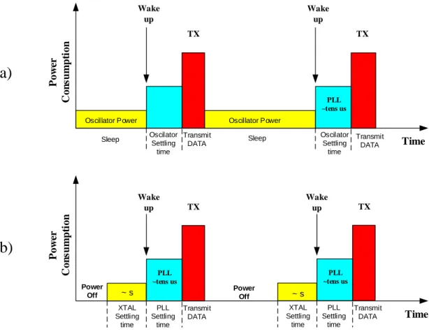
Fig. 1.3: Power schematic of transmitter in
a) Intermittent operation and b) Normally-off operation
P ow er C on su m p ti on Time TX Wake up
Sleep OscilatorSettling time Transmit DATA TX Wake up PLL ~tens us P ow er C on su m p ti on Time TX Wake up Power Off PLL Settling time PLL ~tens us Transmit DATA XTAL Settling time ~ s TX Wake up Power Off PLL Settling time PLL ~tens us Transmit DATA XTAL Settling time ~ s Sleep Oscilator Settling time Transmit DATA Oscillator Power Oscillator Power
a)
b)
5
[1-7]. There is a range of approaches for resolving this issue is proposed in [1-7 - 1-15] such as collecting energy from ambient environment [1-7 – 1-10, 1-15], routing algorithm [1-11, 1-12], developing power management method [1-13, 1-14, 1-15], etc. One of the most interesting technique to prolong the WSNs lifetime is Energy Harvesting (EH) in which the sensor nodes can recharge their batteries by harvesting renewable energy from ambient environment, such as sunlight, vibration, wind, radio signal and so on, then store it in a battery or super-capacitor [1-16]. This helps WSNs operate quasi-perpetually due to the large number of recharge cycles while the surrounding energy source is nearly unlimited.
Regularly, EH circuits often harvest and buffer energy, then produce for the SN operating as soon as sufficient energy is banked. As energy is not always available or it takes time for harvesting and buffering enough energy to do a useful amount of work, operation in EHSN is usually intermittent [1-15]. Another effective operation mode for EHSN is deploying normally-off radio TRX, which directly cuts down the power consumption of the TRX. Both intermittent and normally-off operation are the ways of computing which switch to sleep mode or aggressively powers off components of computer systems when they need not to operate [1-13, 1-15, 1-16]. The authors in [1-9, 1-10] applied and develop normally-off operation mode to BEAT sensor network which shows a very low power consumption.
0 1 2 3 4 5 6
Conventional Operation Normally-off MCU architecture T ota l P ow er Consumption [mJ ]
Fig. 1.4: Power consumption comparison between conventional
6
Moreover, the low-power sensor node using normally-off MCU architecture in [1-14] can reduce its power consumption by around 70% (Fig. 1.4). In [1-16], thanks to intermittent operation, the RX consumes only a half power in comparison with full-time operation. The power schematic of TX in intermittent and normally-off operation mode are shown in Fig. 1.3. With intermittent operation in Fig. 1.3a), SN often sleeps with small power consumption when no data needs to be sent. As soon as it needs send a data, the oscillator is waken-up firstly then TX will transmit the data. As can be seen from Fig. 1.3b), when there is no data needs to be sent, the TX in the sensor node is in power-off state for saving energy. Whenever the TX needs to send data to other nodes, it will be powered up to transmit data through wireless channel. In both cases, carrier oscillator of the TX require a time duration to start-up before becoming stable to transmit data. This settling time can be short or long, which is depends on what kind of oscillator is deployed. Anyways, it is obvious that the longer start-up time of oscillator is, the more power TX is consumed definitely. Hence, finding out a solution to reduce start-up time of TX carrier oscillator promises much power consumption cut-down.
1.1.3 Interference in wireless communication – Radio regulations
Inside WSN
External Interference Sources
7
Wireless system designers always have to cope with interferences from both natural sources and other users of medium [1-18]. Especially, advances of technologies make demand of connections become more and more, which leads to a scenario that any wireless system has to live with interference created by other systems in the vicinity (Fig. 1.5). Besides, as the fact that exploiting very high frequency applications up to hundreds GHz or beyond face to many tough challenges, radio frequency is a valuable and limited resources. For example, 2.4 GHz ISM band is the most widely used frequency by applications of WiFi, ZigBee, short-range communication, and so on. Such a fact makes wireless systems have to share the same frequency band, which is easily to create negative effects on other systems. Bad impacts of interference often make performance of WSNs become worse, from reducing quality of services to congest the communication, even blocking the communication in WSNs. Therefore, all wireless systems must be robust against interference from other systems.
As regarded above, sharing common valuable frequency resource easily creates interferences to other same frequency band. In principle, the stronger desired signal power in comparison with the interferences, the less negative effects on the system are. However, that can result in a race of increasing TX power, which makes the situation become worse and worse. That such fact demands a radio regulations to guarantee that wireless systems can operate functionally with less bad effects from the others. Hence, while developing wireless systems, designers have to consider to not violate the radio regulations.
1.2 Purpose of the study
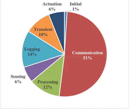
It is noticeable that most energy of a sensor node is consumed in transmission and reception data by its radio TRX. A study in [1-5] shows that about 77.5% of total sensor node energy
Component Percentage (%)
Sensor 6.8
CPU 15.7
Transceiver 77.5
Total 100
8
is spent by the radio TRX (Table 1.1). In other work in [1-19] estimated the energy consumption for communication, processing, transient, sensor loggings and sensing of a low-energy adaptive clustering hierarchy sensor node. The pie chart describing of components is shown in Fig. 1.6. It is easy to realize from this pie that more than a half of total sensor node energy is spent on wireless communication.
In major of WSNs study, main energy sources supplying for the sensor node are portable and limited sources such as battery or energy harvesting (EH) circuits. This can lead to a situation that whenever power source becomes exhausted, the sensor node no longer complete its duty unless the power source is replenished. Besides, battery-powered WSNs also reveal other disadvantages such as inconvenience in replacing for numerous number of sensor nodes, capability of posing an environment risk, etc. EH-WSNs accumulating power from renewable source in ambient environment is an excellent solution to address the battery issue. However, even in that such case, power supply still is not unlimited. Thus, it is necessary to use the power effectively to prolong the sensor nodes lifetime.
There are various methods which were proposed to increase lifetime of sensor nodes, in which reducing power consumption of radio TRX, including both TX and RX, is the best
Fig. 1.6: Power distribution in the low-energy adaptive
clustering hierarchy sensor node
Initial 1% Communication 51% Processing 12% Sensing 6% Logging 14% Transient 10% Actuation 6%
9
effective and directly way to improve sensor node lifetime. Dealing with this issues demands designers to consider a combination of following issues:
Modulation scheme
This is one of the most effective factor to reduce power of TRX system. It completely decides the structure of TRX is complex or low-complex, which directly effects on the power consumption of TRX. The simpler modulation scheme, the more power consumption cut-down.
Operation mode
This controls the way TRX operate. It decides whether TRX works continuously or intermittent or periodically, or in cooperation with wake up receiver and so on.
Frequency band
This has effects on the selection of device technology and circuit topologies. Also, it constrains the specification of TRX system under the radio regulations at that frequency band.
Low power architecture and circuit
Basing on the modulation scheme considered above, the architecture of TRX is sketched. To deploy TRX corresponding to the designed structure, low power circuit topologies are considered and exploited carefully.
Device technology
It is obvious that development of RF TRX is always accompany with the pace of device technologies. Designers need to consider to select the best suitable and feasible technology for their design.
Besides, in circumstance that there are a lot of co-allocated RF devices operate simultaneously, robustness against noise and interference from environment and other RF systems is a crucial metric needs to be considered. These unwanted signals can come from other TXs sending in the same band at the same time (multiple access interference) or from other devices such as microwave ovens, these create co-channel interference. Adjacent-channel interference works in a neighbor band of TRX can inject a part of it power to TRX because of poor-slope filters [1-5]. All of them can make errors for TRX operation, this often is estimated via symbol or bit error rate (SER or BER). SER or BER of TRX system depends
10
on the actual modulation scheme and on the ratio of the received signal power and the noise and interference power (SNIR). In theory, the lower SNIR is, the smaller SER or BER is. There are some solutions for TRX robustness against interference such as using angle modulation (frequency and phase modulation) or utilizing coherent receiver or applying spread spectrum technique. These solutions produce not only good resistance against interference but also excellent sensitivity. However, they cost complex structure and as a consequence, consume more power.
Thus, addressing this trade-offs between low power operation and robustness against interference is one of the purposes of this study.
In addition, this study also concerns about the communication range of the TRX system according to the range of WSN applications. Theoretically, communication distance can be increased by raising TX output power, RX sensitivity and gain of the antenna. Consider in the case of same antenna, we can lengthen communication range by increasing TX output power or enhancing RX sensitivity or both. Regarding to the former solution, increasing output power of TX can be done easily but the downside of this is that TRX system can suffer violence the radio regulations. On the other hand, improving sensitivity is very popular but it often costs more power consumption. These trade-offs also are the other objective of this study.
In general, in this study, we focus on finding the solutions to design a TRX system with low power consumption, robustness to interference and good communication range which is used for low power WSNs.
1.3 Dissertation layout
The dissertation composes of seven chapters as followed:
Chapter 1 gives an overview of WSNs in terms of requirements, specifies the purpose of the study and the challenges need to be addressed to fulfill the objective.
Chapter 2 present the consideration in low power design in terms of modulation scheme, operation mode, architecture and circuit, and device technology to give the solutions to cope with the challenges shown in Chapter 1.
11
Chapter 3 presents a new modulation scheme so-called as Code-Modulation Synchronized-OOK (CMS-OOK) with the waveform, architecture and basic benefits of this scheme
Chapter 4 describes the architecture of CMS-OOK transmitter with low-complexity, suitability to normally-off operation mode. A CMS-OOK TX using sweeping body bias technique based on 65nm SOTB CMOS technology is designed, simulated and evaluated.
Chapter 5 demonstrates architecture of CMS-OOK receiver which allows to increase sensitivity and enhance resistance to interference. A CMS-OOK RX is designed, simulated and fabricated in 65nm SOTB CMOS technology.
Chapter 6 analyze the benefits and consider the suitability of CMS-OOK TRX to low power WSNs.
Finally, Chapter 7 summarizes the research issues and the achieved results; discusses limitations need to continue dealing with in the future.
12
References
[1-1] “Tech Trends 2018: The symphonic enterprise.” [Online]. Available:
https://www2.deloitte.com/content/dam/insights/us/articles/Tech-Trends-2018/4109_TechTrends-2018_FINAL.pdf. [Accessed: 10th Nov. 2018]
[1-2] I. Khan, F. Belqasmi, R. Glitho, N. Crespi, M. Morrow, and P. Polakos, “Wireless Sensor Network Virtualization: A Survey,” IEEE Communication
Surveys & Tutorials, Vol. 18, No. 1, First quarter 2016, pp. 553-576.
[1-3] V. Jindal, “History and Architecture of Wireless Sensor Networks for Ubiquitous Computing,” International Journal of Advanced Research in
Computer Engineering & Technology (IJARCET), Vol. 7, Issue 2, Feb. 2018,
pp. 214-217.
[1-4] C. Chong and S. P. Kumar, “Sensor Networks: Evolution, Opportunities, and Challenges,” Proceedings of the IEEE, Vol. 91, No. 8, Aug. 2003, pp. 1247-1256.
[1-5] H. Karl, and A. Willig, “Protocols and architectures for Wireless Sensor Networks,” John Wiley && Sons, West Sussex, England, 2005.
[1-6] A. E. Zonouz, L. Xingm, V. M. Vokkarane, Y. L. Sun, “Hybrid wireless sensor networks: a realiability, cost and energy-aware approach,” Journals IET
Wireless Sensor Systems, Vol.6, Iss. 2, Jan. 2016, pp. 42-48.
[1-7] V. Shakhov, “On efficiency Improvement of Energy Harvesting Wireless Sensor Networks,” 39th International Conference on Telecommunications and
Signal Processing (TSP), 2016, pp. 56-59.
[1-8] S. Ulukus, A. Yener, E. Erkip, O. Simeone, M. Zorzi, P. Grover, and K. Huang, “Energy Harvesting Wireless Communications: A Review of Recent
13
Advances”, IEEE Journal on Selected Areas in Communications, Vol. 33, No. 3, pp. 360-381, March 2015.
[1-9] S. Ishigaki and K. Ishibashi, “Power Beat: A Low‐cost and Energy Harvesting Wireless Electric Power Sensing Scheme for BEMS,” IEEE ICBEST 2015, Aug 2015.
[1-10] R. Takitoge and K. Ishibashi et. al., “Temperature Beat: Persistent and Energy Harvesting Wireless Temperature Sensing Scheme,” IEEE SENSORS 2016, Nov. 2016.
[1-11] P. Kaushik, J. Singhai, “Energy Efficient Routing Algorithm For Maximizing the Minimum Lifetime of Wireless Sensor Network: A Review,” Intenational
Journal of Ad hoc, Sensor & Ubiquitous Computing (IJSUC) Vol.2, No.2, pp.
25-36, June 2011.
[1-12] J. H. Chang, L. Tassiulas, “Maximum Lifetime Routing in Wireless Sensor Networks, IEEE/ACM Transactions on Networking,” Vol. 12, No.4, August 2004, pp. 609-619.
[1-13] H. Nakamura, T. Nakada, and S. Miwa, “Normally-Off Computing Project: Challenges and Opportunities,” 19th Asia and South Pacific Design Automation Conference (ASP-DAC), pp. 1-5, Jan. 2014.
[1-14] M. Hayashikoshi, H Ueki, H. Kawai, and T. Shimizu, “Normally-Off MCU Architecture and Power Management Method for Low-Power Sensor Network,” 2015 International SoC Design Conference (ISOCC), Nov. 2015, pp. 151-152.
[1-15] B. Lucia, V. Balaji, A. Colin, K. Maeng, abd E. Ruppel, “Intermittent Computing: Challenges and Opportunities,” 2nd Summit on Advances in
14
[1-16] T. Terada et. al., “A CMOS UWB-IR Receiver Analog Front End with Intermittent Operation,” 2007 Symposium on VLSI Circuits Digest of Techincal
Papers, 2007, pp. 86-87.
[1-17] M. A. Khan, Z. A.Khan, S. Ahmed, F. Haldi, and S. H. Ahmed, “Toward Energy Harvesting in Wireless Sensor Networks,” IEEE The 4th HCT
Information Technology trends (ITT2017), Dubai, UAE, Oct. 2017.
[1-18] C. Rose, S. Uluku, and R. D. Yates, “Wireless Systems and Interference Avoidance,” IEEE Transactions on Wireless Communications, Vol. 1, No. 3, July 2002, pp. 415-428.
[1-19] M. N. Halgamuge, M. Zukerman, and K. Ramamohanarao, “An estimation of sensor energy consumption,” Progress In Electromagnetics Research B, Vol.12, 2009, pp. 259-295.
15
Chapter 2
Considerations of Wireless Sensor Networks for Low Power,
Longer Communication Distance and Immunity to Interference
In this Chapter, some issues of low power consumption, lengthening communication distance and enhancing immunity to interference of TRX are considered. Basing on that, some potential solutions will be proposed and considered to apply.
2.1 Low power TRX design
Designing radios with ultra-low-power consumption is always an attraction and challenge to RF designers. It can enable a lot of new and exciting applications such as WSNs, IoTs and so on. As RF TRXs often consume most of the power budget in small SNs [2-1], decreasing TRX power consumption is a useful way to reduce device size as well as increase lifetime of SNs. In principle, RF TRX designing often must deal with numerous trade-offs, that is a complex relationship between power, sensitivity, noise, frequency, gain, linearity and supply voltage. Thus, cutting down radio power can be challenging. For purpose of low power, designers must consider to sacrifice one or more other metrics.
2.1.1 Link budgeting
Consider a representative WSN system operating with 2.4GHz carrier frequency in short range communication. The minimum TX output power can be calculated based on Friis equation for free space as a baseline case [2-2]:
16
𝑃𝑟𝑒𝑐𝑒𝑖𝑣𝑒𝑟 = 𝑃𝑡𝑟𝑎𝑛𝑠𝑚𝑖𝑡+ 𝐺𝑎𝑛𝑡𝑒𝑛𝑛𝑎+ 20 log10
𝜆
4𝜋𝑑 (2 − 1) where λ is the carrier wavelength and d is the distance between TX and RX. According to equation (2-1), in free space a 10m link suffers from about 60dB of path loss at 2.4GHz band. With a typical surface mount antenna for 2.4GHz has a gain of 0dBi and other reasons can make TX signal experience as much as 30dB loss, TX should have output power of 0 dBm [2-3]. In order to achieve successful operation of TRX, the condition of “Preceiver is higher
than RX sensitivity” must be guaranteed. Maximum communication distance is fulfilled under condition of Psensitivity = Preceiver is satisfied. Therefore, communication distance d can
be raised by increasing power of TX or increasing sensitivity of RX. It is notice that increasing power of TX must guarantee to not violate the radio regulations while improving sensitivity of RX often cost more power consumption by using LNA and RF amplifiers.
2.1.2 Modulation scheme and architecture
To achieve low power operation, designer has to optimize across all design layers from modulation scheme, architecture to circuits and devices. One of the most effective way to reduce power is decreasing the complexity of modulation scheme which leads to make architecture of TRX become simpler. Conventional super-heterodyne TRX architecture
17
often adopts quadrature amplitude modulation (QAM) or angle modulation [2-3]. Although, this structure has a lot of advantages, it also brings more additional complexities into TRX system such as phase-locked loop (PLL), high-linear power amplifier (PA). Of course, this means the power of TRX increases.
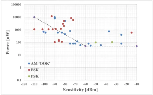
Employing a non-coherent modulation scheme such as On-Off Keying (OOK) can significantly simplify the architecture of TRX, such as eliminating the PLL, using nonlinear but high efficiency PAs which allows to reduce further power consumption. Hence, low power TRX designers have trend of utilizing OOK modulation scheme with low-complexity architecture as shown in Fig. 2.1. For the same reason, RX structure with envelope detector or super regenerative is prefer. However, adopting this kind of modulation scheme with low-complexity architectures has to face to trade-offs performance in terms of sensitivity, spectral efficiency, resistance to interference etc. Fig. 2.2 shows a low power radio survey in recent time [2-4 – 2-18]. As can be seen, most of OOK RX consumes lower power in comparison with FSK and PSK RX.
This study endeavors to achieve better spectral efficiency, immunity to interference at low power operation.
Fig. 2.2: Power versa sensitivity radio survey
0.1 1 10 100 1000 10000 100000 -120 -110 -100 -90 -80 -70 -60 -50 -40 -30 -20 -10 P o w er [uW] Sensitivity [dBm] AM 'OOK' FSK PSK
18
2.1.3 Operation mode
Normally, the active power of TXs is usually much higher than that of RX [2-19]. Thus, one of the best way to reduce power consumption of TRX is cutting down power consumption of TX. Intermittent and normally-off operations which are discussed in Chapter 1 are the most directly efficient solutions. In order to achieve reducing energy with this operation mode, carrier oscillator of TX must be designed in such a way that TX will completely turn-off or consume a tiny power when no data is sent but wake-up quickly from power-down state to start transmitting data. A comparison between settling time of a ring oscillator, two PLL oscillators and a crystal oscillator is carried on and the comparison results are exhibited in Table 2.1. Obviously, the RO has the shortest-settling time in comparison with other kinds of oscillator, which indicates that RO is completely suitable to intermittent and normally-off operation.
It is popular that OOK TRXs often utilize ring oscillator as carrier source. Besides, as regarded in previous section that OOK modulation scheme is usually preferred for low power purpose. This suggests that OOK TRXs using ring oscillator with low power and short-settling time can reduce huge power when they operate in normally-off or intermittent mode.
2.2 Spread-spectrum technique
SS communications with its inherent interference attenuation capability and low peak power spectral density has been very popular. These crucial features of SS technique are noticeable for finding solutions to improve immunity to interference of TRX and increase the power of TX while still ensure to meet radio regulations.
Table 2.1: Settling time comparison ISSCC'15 [2-20] IRFICS'18 [2-21] LoRa [2-22] JSSC'16 [2-23] Type of Oscillator PLL PLL Crystal Ring Oscillator
Settling time 15µs 0.4µs 250µs 0.5ns Frequency Accuracy High High High Low
19
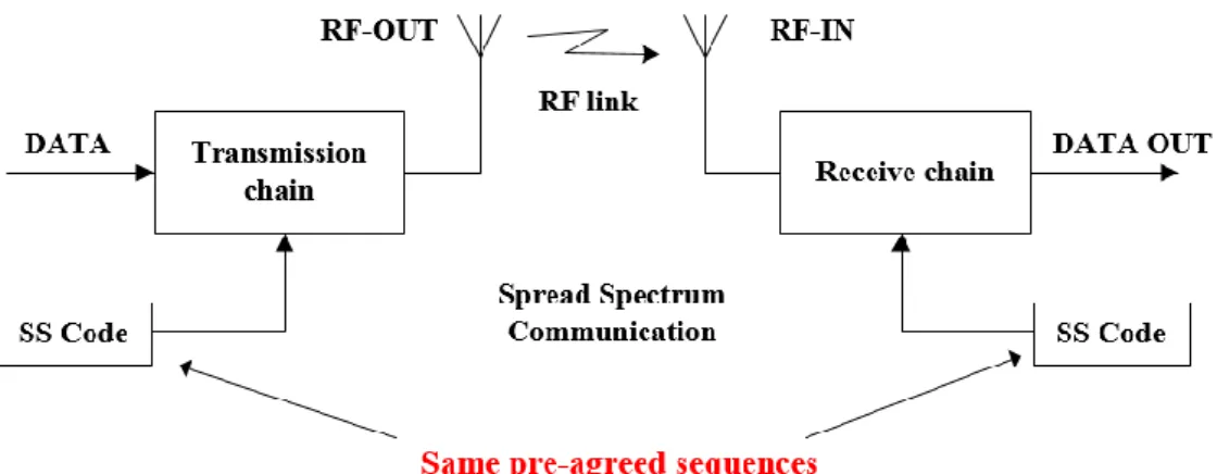
Several of the techniques are “direct-sequence SS” (DS-SS) modulation in which a fast pseudo-randomly generated sequence is multiplied with low rate DATA need to be sent, “frequency hopping SS” (HFSS) in which the carrier is caused to shift frequency in a pseudorandom way and “time hopping SS” wherein burst of signal are initiated at pseudorandom time [2-24, 2-25]. Among them the first is the simplest in implementing the hardware.
A simple SS communication channel is shown in Fig. 2 [2-26]. It is noticeable that the SS RX must pre-understand the code of the TX. So that the RX can demodulate to recover data by using matched filter. RX can utilize analog matched filter or digital matched filter depending on the situation. RX with analog matched filter can receive SS signal from TX with very low SNR and TXs can use the same frequency band to communicate without making interference to the others. However, structure of analog matched filter is complex according to high power consumption. For low power operation, digital matched filter which is deployed in digital circuit is more reasonable, but it cost limitation of interference resistance. This will be discussed more in Chapter 6.
Besides, as soon as SS technique is used for TRX system, it produces wider bandwidth signal and process gain which helps sensitivity of RX increase. Sensitivity of a SS communication system is calculated as below [2-24, 2-25]:
𝑃𝑠𝑒𝑛𝑠𝑖𝑡𝑖𝑣𝑖𝑡𝑦[𝑑𝐵𝑚] = 𝑁𝐹(𝑑𝐵) + 𝑘𝑇𝐵𝑅𝐹[𝑑𝐵𝑚] +
𝐸𝑏
𝑁0[𝑑𝐵] − 𝑃𝐺(𝑑𝐵) (2 − 2)
20
where NF is noise figure of RX, k = 1.38∙10-23 J/K is Bolztmann constant, T = 290K at room
temperature, BRF is RF carrier bandwidth in Hz which is equal to chip rate for the SS system,
Eb/N0 is signal to ratio (SNR) corresponding to a given bit error rate (BER), PG is process
gain which is calculated by the ratio between code rate and data bit rate. Hence, we can rewrite above equation for SS system operates at room temperature as followed:
𝑃𝑠𝑒𝑛𝑠𝑖𝑡𝑖𝑣𝑖𝑡𝑦[𝑑𝐵𝑚] = −174 + 𝑁𝐹(𝑑𝐵) + 10𝑙𝑜𝑔𝐵𝑅𝐹[𝐻𝑧] +
𝐸𝑏
𝑁0[𝑑𝐵] − 𝑃𝐺(𝑑𝐵) (2 − 3)
Comparing with sensitivity of general RX which is calculated according to equation (2-4) [2-26]:
𝑃𝑠𝑒𝑛𝑠𝑖𝑡𝑖𝑣𝑖𝑡𝑦[𝑑𝐵𝑚] = −174 + 𝑁𝐹(𝑑𝐵) + 10𝑙𝑜𝑔𝐵𝑅𝐹[𝐻𝑧] +
𝐸𝑏
𝑁0[𝑑𝐵] (2 − 4) It is easy to realize that with the same bandwidth of signal, SS RX can improve the sensitivity by process gain PG [dB]. Thus, this study intends to apply spread spectrum technique to the proposed TRX system in order to exploit its advantage of excellently withstanding to interference.
2.3 RF Characteristics of 65nm SOTB CMOS Device
The Silicon-On-Thin Buried Oxide (SOTB) CMOS, which is one of the FD-SOI CMOS processes, has been developed recently with a lot of advantages in comparison to
21
conventional BULK CMOS [2-27 - 2-29]. These merits indicate that the SOTB CMOS is a brilliant candidate for low voltage, low-power applications [2-30, 2-31].
Figure 2.4 shows the cross section of SOTB CMOS devices [2-28, 2-29]. Unlike conventional SOI CMOS with a thick BOX layer, SOTB CMOS has much thinner BOX thickness of about 10nm and has deep Nwell layer, thus the body voltages of PMOS and NMOS can be controlled separately. As a result, designers can control operation of circuits using SOTB devices easily by adjusting body bias voltage. Changing in body bias voltages
SOTB CMOS
Fig. 2.5: Chip photo of investigated SOTB
CMOS
Fig. 2.6: Measured FT and Fmax of 65nm SOTB CMOS at Vd = 1.2V, Vg = 0.65V, Vb = 0 for NMOS
22
is consequence in variation of threshold voltage of SOTB devices, and then of devices operation. This feature is very useful because it helps us change frequency of a based-on SOTB devices oscillator circuit by varying body bias voltage of NMOS and PMOS.
Besides, being a kind of SOI device with small drain conductance SOTB devices help analog circuits using them can operate at low voltages [2-30]. Whereby, SOTB devices are commensurate with low power design.
A question that is SOTB device suitable to RF circuit design or not? To answer this question, we, firstly, investigated RF characteristics of SOTB NMOS and PMOS. A couple of 8-finger SOTB NMOS and PMOS with same size of 6um width (48um total width) and 60nm length were laid-out, fabricated and evaluated. Micrograph of the fabricated CMOS chip is exhibited in Fig. 2.5.
Evaluation of SOTB CMOS RF characteristics was carried out under followed conditions: Vd = 1.2V, Vg = 0.65V, Vb = 0 for NMOS and Vd = - 1.2V, Vg = -0.65V, Vb = 0
for PMOS. Measured results of the cut-off frequency FT and the maximum oscillation
frequency Fmax of the CMOS are shown in Fig. 2.6. It is easy to see that the SOTB NMOS
owns quite high FT and Fmax of 40 GHz and 28 GHz, respectively, while those of PMOS are
consequently smaller values of 26 GHz and 20GHz [2-31]. In comparison to operation frequency 2.4GHz of proposed CMS-OOK TRX in this study, these values are much higher. This guarantees that 65nm SOTB CMOS is capable of implementing well for 2.4 GHz band application designs.
2.4 Conclusion
In this Chapter, consideration of TRX system in terms of power, communication distance and immunity to interference is present.
In order to reduce power consumption of TRX, intermittent and normally-off operation of TX is selected in combination with utilizing low-complexity architecture of OOK TRX. 65nm SOTB CMOS devices are chosen for implementing physical TRX system because of its excellent advantages. Especially, body bias control of SOTB CMOS can
23
diffuse spectrum of carrier frequency, which results in spreading spectrum of TX output signal. Whereby, bandwidth efficiency of the TRX is improved.
Regarding to lengthening communication distance, solutions to increase TX output power and RX sensitivity are considered. Among them, spread spectrum technique by code modulation in combination with sweeping carrier frequency by controlling body bias voltage of SOTB devices are applied. Thanks to this combination, not only TX output power can be raised without radio regulations violence but also TRX has more process gain to increase sensitivity. Moreover, this also can help TRX improve immunity to interference by widening BW and assigning different codes to different TXs.
Based on above considerations and selections, a new modulation scheme is proposed in Chapter 3 and implementation of a TRX system based on 65nm SOTB CMOS technology was carried out and evaluated in Chapter 4 and Chapter 5.
24
References
[2-1] J. M. Rabaey, J. Ammer, T. Karalar, S. Li, B. Otis, M. Sheets, T. Tuan, “PicoRadios for wireless sensor networks: The next challenge in ultra-low power design,” IEEE International Digest of Technical papers, Solid-State Circuits
Conference, 2002, pp. 2001-2002.
[2-2] H. T. Friis, “A note on a simple transmission formular,” Proceeding s of the I. R.
E. and Waves and Electrons, May 1946, pp. 254-256.
[2-3] H. Karl, and A. Willig, “Protocols and architectures for Wireless Sensor Networks,” John Wiley && Sons, West Sussex, England, 2005.
[2-4] J. Bae et al., “A 490 uW fully MICS compatible FSK transceiver for implantable devices,” 2009 Symposium on VLSI Circuits Digest of Technical Papers, pp. 36– 37
[2-5] S. Wu, B. Razavi, “A 900-MHz/1.8-GHz CMOS receiver for dual-band applications,” IEEEJ.Solid-State Circuits 33, 2178–2185 (1998)
[2-6] M. Vidojkovic et al., “A 0.33 nJ/b IEEE802.15.6/proprietary-MICS/ISM band transceiver with scalable data-rate from 11 kb/s to 4.5 Mb/s for medical applications,” ISSCC,2014, pp. 170–172
[2-7] S. Chakraborty et al., “An ultra-low power reconfigurable multi-standard transceiver using fully digital PLL,” Proc. Symp. VLSI Circuits, June 2013, pp. 148–149
[2-8] R. Kumar et al., “A fully integrated 2x2 b/g and 1x2 a-band MIMO WLAN SoC in 45nmCMOS for multi-radio IC,” ISSCC, 2013.
[2-9] J. Masuch et al., “A 1.1 mW RX 81.4 dBm sensitivity CMOS transceiver for Bluetooth low energy,” IEEE Trans. Microw. Theory Tech. 61, 1660–1673 (2013)
25
[2-10] Y.H. Liu et al., “A 2.7 nJ/bit multi-standard 2.3/2.4 GHz polar transmitter for wireless sensor networks,” ISSCC Dig. Tech. Papers, February 2012, pp. 448– 450
[2-11] R.E. Crochiere, L.R. Rabiner, “Multirate Digital Signal Processing,” Prentice-Hall Inc., Englewood Cliffs, New Jersey 07632 (Prentice Prentice-Hall, 1983)
[2-12] T. Ha, S. Lee, J. Jim, “Low-complexity correlation system for timing synchronization in IEEE802.11a wireless LANs,” in Proceedings of Radio and
Wireless Conference, 2003
[2-13] J.C. Roh, A. Batra, S. Hosur, “Packet detection and coarse symbol timing for rotated differential M-ary PSK modulated preamble signal,” US Patent 8,630,374 [2-14] H.-S. Kim, S.-J. Lee, M. Goel, “Method, device, and digital circuitry for providing a closed-form solution to a scaled error locator polynomial used in BCH decoding,” US Patent 8,392,806
[2-15] P. Reviriego, C. Argyrides, J.A. Maestro, “Efficient error detection in Double Error Correction BCH codes for memory applications,” Microelectron. Reliab.
52(7), 1528–1530 (2012)
[2-16] J. Kwong, Y.K. Ramadass, N. Verma, A.P. Chandrakasan, “A 65 nm sub-Vt microcontroller with integrated SRAM and switched capacitor DC–DC converter,” IEEE J. Solid-State Circuits 44(1), 115–126 (2009)
[2-17] R. Tabrizian et al., “A 27 MHz temperature compensated MEMS oscillator with sub-ppm instability,” in IEEE 25th Int’l Conf. on Micro-Electro Mechanical
Systems (MEMS), 29th January - 2nd February 2012, pp. 23–26
[2-17] N. Fletcher, J.M. Rabaey, “Ultra-Low Power Wakeup Receivers for Wireless Sensor Networks,” (EECS Department, University of California Berkeley, 2008)
26
[2-18] X. Huang, S. Rampu, X. Wang, G. Dolmans, H. de Groot, “A 2.4 GHz/915 MHz 51 W wake-up receiver with offset and noise suppression,” in IEEE Solid-State
Circuits Conference, February 2010.
[2-19] M. T. Hoang, “A study on ultra-low power and high sensitivity OOK CMOS RF Receiver for Wireless Sensor Networks,” Doctoral thesis, the University of Electro-Communications, 2015.
[2-20] Y. H. Liu et al., “A 3.7mW-RX 4.4mW-TX fully integrated Bluetooth Low-Energy/IEEE802.15.4/proprietary SoC with an ADPLL-based fast frequency offset compensation on 40nm CMOS,” ISSCC, Feb. 2015, pp. 236-237.
[2-21] X. Chen, J. Breiholz, F. Yahya, C. Lukas, H. S. Kim, B. Calhoun, D. Wentzloff, “A 486µW All-Digital Bluetooth Low Energy Transmitter with Ring Oscillator Based ADPLL for IoT Applications,” IEEE Radio Frequency Integrated Circuits
Symposium, 2018, pp.168-171.
[2-22] SX1276/77/78/79 datasheet, Semtech Cor. [Online]. Available:
https://www.semtech.com/uploads/documents/DS_SX1276-7-8-9_W_APP_V5.pdf. Accessed: 10th Nov. 2018
[2-23] W. Bae, H. ju, K. Park, S. Y. Cho, and D. K. Jeong, “A 7.6mW, 414 fs RMS-jitter 10Ghz Phase Locked Loop for a 40 Gb/s Serial Link Transmitter Based on a Two-Stage Ring Oscillator in 65nm CMOS,” IEEE Journal of Solid-State
Circuits, No. 10, Oct. 2016, pp. 2357-2367
[2-24] J. S. Lee, and L. E. Miller, “CDMA Systems Engineering Handbook,” Artech
House Publishers, 1998.
[2-25] S. C. Yang, “CDMA RF System Engineering,” Artech House Publishers, 1998. [2-26] B. Razavi, “RF Microelectronics,” Pearson Education, Inc., 2012
27
[2-27] R. Tsuchiya et al., “Silicon on thin box: a new paradigm of the CMOSFET for low-power high-performance application featuring wide-range back-bias control,” IEEE International Electron Devices Meeting, Dec. 2004, pp. 631-634 [2-28] T. Ishigaki, “A study on Silicon-on thin-Box (SOTB) CMOSFET for low power
LSIs,” Doctoral Thesis, Tokyo Institute of Technology, 2012.
[2-29] S. Morohashi, N. Sugii, C.K. Pham, K. Ishibashi et. al., “10MHz 44µW Operation Power, 4.2nA Sleep Current 50K Gate Logic Design using Adjustable Vb for SOTB devices,” IEEE S3S Conference, 2013.
[2-30] K. Ishibashi, N. Sugii et al., “A perpetuum mobile 32 bit CPU with 13.4 pJ/cycle, 0.14 lA sleep current using reverse body bias assisted 65 nm SOTB CMOS technology,” Cool chip XVII Conference, pp. 1–3, 2014.
[2-31] V. T. Nguyen, R. Ishikawa, and K. Ishibashi, “83nJ/bit Transmitter Using Code-Modulated Synchronized-OOK on 65nm SOTB for Normally-Off Wireless Sensor Networks,” IEICE Trans. On Electronics, Vo1. E101-C.472 Jul. 2018, pp. 472-472
28
Chapter 3
Proposal of Code-Modulated Synchronized – OOK
Modulation Scheme
In order to achieve ULP operation, it is necessary to optimize across all design layers, ranging from modulation schemes and architectures to circuits and devices. One of the most efficient ways to reduce power is to decline the complexity of the modulation schemes, which normally also decreases the overall architectural complexity [3-1]. According to a survey on energy efficient modulation and coding techniques for WSNs, the modulation and coding process are very important to improve the energy efficiency and BW efficiency of a wireless networks. It is popular that non-coherent modulation scheme such as OOK and FSK are mostly modulation used in sensor node radio TRXs. These schemes not only greatly simplify the architecture of TRX but also are compatible with nonlinear but high efficient PAs [3-2], which enable a further reduction in power consumption. In which, direct-modulation TX architectures utilizing OOK direct-modulation scheme and RX with envelope detector or super-regenerative architectures are prefer. Besides ULP issue, in the fact that there are a lot of radio devices operating simultaneously in the vicinity of the TRX [1, 3-2]. In this scenario, improving reliability of TRX means enhancing the resistance to interference. In this section, we propose a Code-Modulated Synchronized-OOK (CMS-OOK) scheme which helps us not only reduce power consumption but also enhance immunity to interference.
29
3.1 Synchronized-OOK modulation
The Synchronized-OOK modulation scheme is firstly witnessed in the Impulse-Radio Ultra Wide band (IR-UWB) TRXs of M. Crepaldi [3-3], and then is used in the TRXs system of M. T. Hoang in [3-4]. Theoretically, in the conventional OOK modulation, RF carrier appears during whole duration of data ‘1’ and absents from time of data ‘0’ (Fig. 3.1a). In difference to this, S-OOK signal is established by two kinds of pulse: synchronized pulse and data pulse. According to this, data ‘1’ is displayed by two pulses including a synchronized pulse and a data pulse, while data ‘0’ is represented by only one synchronized pulse (Fig. 3.1b).
Fig. 3.1a) shows the waveform of a data needs to be sent (DATA) and the corresponded conventional OOK RF signal. It is easy to realize that RF carrier signal appears continuously during data ‘1’ pulse width, Tb. Thus, OOK TX here consumes power during
this time. On the other hand, the sent data (DATA), OOK baseband signal (SDATA) and S-OOK RF signal are described in Fig. 3.1b). This figure informs that S-S-OOK TX only expends power during only duration of synchronized pulse and data pulse Tp, which is much smaller
than Tb. As a result, to send a data at the same rate with the condition that OOK TX and
S-OOK TX have same average power Pavg, the energy is used for transmitting a pair of data
‘1’ and data ‘0’ of S-OOK TX is Tb/3Tp times lower than that of OOK TX. With Tp is much
shorter than Tb, S-OOK TX swallows much smaller energy than OOK TX does. Besides,
Fig. 3.1: a) Conventional OOK signal
30
this also leads to another effect that BW of S-OOK RF signal is wider than that of OOK RF signal.
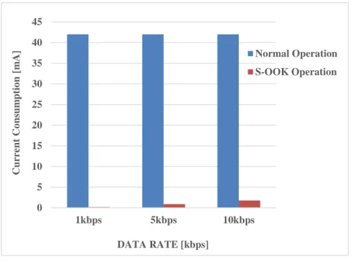
In [3-4], authors implemented and evaluated S-OOK RX chip based on 65nm SOTB CMOS technology. It is noticeable that complicated clock and data recovery circuit are vanished from the S-OOK RX. Moreover, the RF circuits in the RX can be heavily duty-cycled using a narrow window, known as RFENABLE duration. These help RX nearly consume no power in duration between synchronized pulses and data pulses. Thanks to these techniques, S-OOK RX produced -58dBm sensitivity and 1.36uW power consumption at 10kbps data rate.
The benefit of power efficiency of S-OOK scheme can be seen through the chart in Fig. 3.2. In comparison with normal operation at the same data rate, S-OOK RX consumes nearly 90% lower power.
On the other hand, S-OOK modulation exposes some disadvantages. First, as it is necessary to use 2 RF pulses to represent a bit, data rate is limited and usually pre-determined. Second, less complex architecture of RX provided good power consumption but poor
Fig. 3.2: Current consumption of the S-OOK RF front-end
0 5 10 15 20 25 30 35 40 45 1kbps 5kbps 10kbps C urre nt C o ns um ptio n [m A ] DATA RATE [kbps] Normal Operation S-OOK Operation
31
sensitivity. Finally, it is noticeable that S-OOK essentially is a special case of OOK modulation. Thus, reliability of S-OOK TRX system is reduced in presence of interference. It also demands a method to synchronize data pulse and synchronized pulse.
3.2 Spread-Spectrum communications and Direct-Sequence Spread-Spectrum technique
Spread-spectrum (SS) communications technology was first described on paper by an actress and musician in 1941 and was not taken seriously [3-5]. It even was forgotten until the 1980s, when the came alive and has become increasingly popular with initial applications in military anti-jamming tactical communications, anti-multipath systems and so on. Typical applications for the resulting short-range data TRXs include satellite-positioning systems (GPS), 3G mobile telecommunications, W-LAN (IEEE802.11a, IEEE802.11b, IEE802.11g), and Bluetooth. SS technique is a crucial solution for the endless race between communication demands and radio-frequency availability [3-6].
This technique is defined as follows: “Spread spectrum is a means of transmission in which the signal occupies a bandwidth in excess of the minimum necessary to send the information; the band spread is accomplished by means of a code which is independent of the data, and a synchronized reception with the code at the receiver is used for de-spreading and subsequent data recovery” [3-5].
Direct Sequence Spread Spectrum (DS-SS) is one of three main SS techniques. In such this way, data needs to be sent is spread over a wide band by multiplying with a code sequence (Fig. 3.3). On the transmission path, there are narrower interferences which are
a) b)
![Fig. 1.4: Power consumption comparison between conventional operation and normally-off operation [1-14]](https://thumb-ap.123doks.com/thumbv2/123deta/7729599.1711529/25.892.179.722.144.506/fig-power-consumption-comparison-conventional-operation-normally-operation.webp)