T OKYO C ITY U NIVERSITY
D
OCTORALT
HESISStudy on Design Technique of High
Resolution ADC Using Dynamic Analog
Components
Chunhui PAN
A thesis submitted in fulfillment of the requirements for the degree of Doctor of Engineering
in the
Graduate School of Engineering Department of Information Engineering
March 16, 2019
iii
Abstract
Chunhui PAN
Study on Design Technique of High Resolution ADC Using Dynamic Analog Components
The digital signal processing is performed widely on the computer system and com- munication system. Benefit from digital circuits are robust and can be realized by extremely small and simple structures, the fast, and very complex accurate systems can be implemented. As time goes by, the speed and density of digital integrated circuits is increasing, the dominance of digital system in almost all areas of commu- nications system and consumer products is increasingly obvious. However, humans live in the physical world of analog signals, the data converters are needed to inter- face with the digital signal processing (DSP) system. As the speed and capability of DSP cores increases, the speed and accuracy of the converters associated with DSP have to increases, which led to unprecedented challenges.
Low voltage, high signal-to-noise and distortion ratio (SNDR) ADC analog-to-digital converters (ADCs) are widely used in the mixed-signal system on chip (SoC) in the fields of the wireless sensor network such as human body information measurement, environmental information monitor, interactive multimedia system, consumer de- vice and industrial applications. In recent years, with the feature size of CMOS (Complementary Metal Oxide Semiconductor) devices scaled down, the increasing speed of devices has enabled the ADCs to achieve several tens of MS/s to low GS/s sampling rates. However, the degradation of the transistor is influencing the perfor- mance of the integrated circuit, such as the increase of threshold-voltage mismatch, and the reduction of the intrinsic gain. Moreover, the dynamic range of analog signal
is limited by the low supply voltage. Due to the degradation of the analog circuit lin- earity, the realization of the high-gain amplifier and high-resolution ADC is difficult.
In order to achieve the high energy efficiency of ADC.
In this thesis, the design technique of delta sigma modulator using dynamic analog components is proposed to improve the performance of AD convertor. The dynamic amplifier (ring amplifier) is used to realize the integrator in the proposed delta sigma modulator. Benefit from the bias circuit not requited in the dynamic amplifier, the energy efficiency of delta sigma modulator can be improved. The SAR quantizer with dynamic comparator is used to realize the internal multi-bit quantizer, which not only can relax the slew-rate requirement on the amplifier in the integrator, but also can maintain the high energy efficiency for delta sigma modulator. Moreover, several techniques are proposed for enhance the performance of delta sigma mod- ulator using dynamic analog component. The passive adder embedded noise cou- pling (NC) SAR quantizer is proposed to realize the summation of analog signals, and the quantization error feedback (It can feed the shaped the quantizer noise to the loop filter without the active amplifier) which achieve an addition 1st-order noise shaping without the extra integrator. As a result, a 3rd-order noise coupled delta sigma modulator is realized by two integrators using dynamic amplifier and the proposed noise coupling SAR quantizer, it achieved the greater bandwidth and the better performance (eg. better FOMW and FOMS). Furthermore, a novel implemen- tation of complex integrator circuit is proposed to improve the energy efficiency and to reduce the circuit area of quadrature bandpass delta sigma modulator. The digi- tized noise coupling SAR quantizer is used to realize high order noise shaping and image rejection for the quadrature bandpass delta sigma modulator. By applying the above proposed techniques, a 6th-order QBPDSM with 2nd-order image rejec- tion is realized by two dynamic analog components based complex integrators and the digital domain noise coupling SAR quantizer embedded by passive adder, which achieved the better performance.
v
Acknowledgements
Three years of doctoral candidate career is coming to an end, looking back to the past along the way, it is really hard to describe this feeling with words. Although most of the time were spent in a busy environment, I have made great progress in learning and growing during this period, both in problem solving and in dealing with people. Now I have successfully obtained my doctor’s degree. I am so grateful to all the people who have helped and cared for me in this period.
First, I would like to thank my supervisor, Professor San, thank you for your invalu- able guidance, technical knowledge and support during the study. From master’s program to doctoral program, a total of five years of time, not only he provided me with good study environment, learning resources, and detailed guidance for this re- search, but also cultivated my professional objective research spirit and taught me the way of doing things. I would also like to acknowledge Prof. T. Shibata, Prof. M.
Sawahashi, Prof. K. Sawano and Prof. A. Hyogo for their invaluable advice. Sincere thanks are also extended to my colleagues in the Integrated System Laboratory.
Finally, I would like to thank my parents for their care, support and encouragement during my PhD program. Thank you for your efforts to let me pursue my ideal without any worries, so that I can successfully complete my study. I would also like to dedicate this paper to all those who have helped and cared for me. I hope you can share this honor and happiness with me. In the future, I will try my best to enrich myself and push the limits my strengths so as not to fall short of everyone’s expectations of me.
Chunhui Pan Tokyo City University March 2019
vii
Contents
Abstract iii
Acknowledgements v
1 Introduction 1
1.1 Background . . . 1
1.2 Objectives . . . 7
1.3 Construction . . . 10
References . . . 13
2 Theory of Delta Sigma Modulator 15 2.1 Preface . . . 15
2.1.1 Oversampling . . . 15
2.1.2 Noise Shaping . . . 17
2.2 Mathematical Model of Delta Sigma Modulator . . . 20
2.2.1 Noise Transfer Function . . . 20
2.2.2 Quantization Error Model . . . 21
2.2.3 Calculation of In-Band Noise Power . . . 24
2.3 High Order Delta Sigma Modulator . . . 27
2.3.1 Feed-back Structure . . . 27
2.3.2 Feed-forward Structure . . . 30
2.3.3 Performance Estimation . . . 32
2.4 Summary . . . 33
References . . . 34
3 Delta Sigma Modulator Using Ring Amplifier 35 3.1 Preface . . . 35
3.1.1 Drawback of Conventional Delta Sigma Modulator . . . 35
3.1.2 Concept of Proposed Delta Sigma Modulator . . . 36
3.2 Architecture . . . 36
3.3 Implementation . . . 37
3.3.1 Integrator using Ring Amplifier . . . 37
3.3.2 SAR Quantizer with Passive Adder . . . 46
3.3.3 Data Weighed Average Logic Circuit . . . 49
3.4 Noise Analysis . . . 52
3.4.1 Noise Analysis of Ring Amplifier . . . 52
3.4.2 Noise Analysis of Integrator using Ring Amplifier . . . 53
3.4.3 Noise Analysis of Dynamic Comparator . . . 58
3.5 Simulation . . . 64
3.6 Measurement . . . 64
3.6.1 Layout and Microphotograph . . . 64
3.6.2 Measurement Results . . . 65
3.7 Summary . . . 68
References . . . 68
4 Improved Delta Sigma Modulator Using Ring Amplifier 71 4.1 Preface . . . 71
4.1.1 Drawback of Proposed DSM using Ring Amplifier . . . 71
4.1.2 Design Considerations of DSM using Ring Amplifier . . . 72
4.2 Architecture . . . 74
4.2.1 Structure of Improved Delta Sigma Modulator . . . 74
4.2.2 Transmission Function of Improved Delta Sigma Modulator . . 75
4.3 Implementation . . . 76
4.3.1 Pseudo Differential Ring Amplifier . . . 78
4.3.2 Improved SAR quantizer with Passive Adder . . . 82
4.3.3 Multi-bit DAC and DWA Logic Circuit . . . 87
4.4 Simulation . . . 89
4.5 Measurement . . . 90
4.5.1 Layout and Microphotogragh . . . 90
ix
4.5.2 Measurement Results . . . 91
4.6 Summary . . . 93
References . . . 93
5 3rd-Order Noise Coupled Delta Sigma Modulator 95 5.1 Preface . . . 95
5.1.1 Error Feedback Technique . . . 95
5.1.2 Comparison of Noise Coupling Implement Method . . . 96
5.2 Architecture . . . 96
5.3 Implementation . . . 97
5.3.1 Pseudo Differential Ring Amplifier with improved CMFB . . . 100
5.3.2 Passive Adder embedded QNS SAR Quantizer . . . 102
5.3.3 Multi-bit DAC and DWA Logic Circuit . . . 106
5.4 Simulation . . . 109
5.4.1 Noise Analysis of Integrator with Different DAC . . . 109
5.4.2 Simulation with Thermal Noise . . . 111
5.5 Summary . . . 114
References . . . 115
6 6th-Order Quadrature Bandpass Delta Sigma Modulator 117 6.1 Preface . . . 117
6.1.1 Image Rejection Technique . . . 117
6.1.2 Comparison of Complex Integrator Implement Method . . . 118
6.1.3 Concept of Proposed Quadrature Bandpass DSM . . . 119
6.2 Architecture . . . 121
6.3 Implementation . . . 122
6.3.1 Proposed Complex Integrator Circuit . . . 127
6.3.2 Pseudo Differential Ring Amplifier with Energy Saving . . . 130
6.3.3 Noise Coupling SAR Quantizer . . . 134
6.3.4 Multi-bit DAC and Quadrature-DWA Logic . . . 138
6.4 Simulation . . . 141
6.5 Summary . . . 142
References . . . 143
7 Conclusion 145 7.1 Conclusion . . . 145 7.2 Future Work . . . 150
A SQNR of High Order Delta Sigma Modulator With Multi-bit Quantizer 153
B VerilogA Code 157
C Publication List 173
xi
List of Figures
1.1 FOMS versus CMOS Technology . . . 2
1.2 FOMW versus CMOS Technology . . . 2
1.3 Energy efficiency of ADC . . . 3
1.4 FOMS versus Speed . . . 5
1.5 FOMW versus Speed . . . 5
1.6 Implementation of integrator using ring amplifier . . . 7
1.7 Construction of this dissertation . . . 10
2.1 A typical DSP system with interface circuit . . . 15
2.2 System model of the delta sigma modulator . . . 17
2.3 Block diagram of delta sigma modulator . . . 18
2.4 Block diagram of first-order delta sigma modulator . . . 20
2.5 Transfer function of mid-rise and mid-tread quantizer . . . 22
2.6 Probability density function of the quantization error . . . 23
2.7 Noise transfer function of first-order delta sigma modulator . . . 24
2.8 SQNR versus OSR of first-order delta sigma modulator using the in- ternal quantizer with the different resolution (1∼5bit) . . . 26
2.9 Block diagram of second-order feed-back structure delta sigma mod- ulator . . . 28
2.10 Output waves of integrators in the second-order feed-back delta sigma modulator using 4-bits internal quantizer while the sine signal with an amplitude of±1 V is input (Vreference =1.2V) . . . 29
2.11 Block diagram of second-order feed-forward structure delta sigma modulator . . . 30
2.12 Output waves of integrators in the second-order feed-forward delta sigma modulator using 4-bits internal quantizer while the sine signal
with an amplitude of±1 V is input (Vreference=1.2V) . . . 31
2.13 SQNR of high order delta sigma modulator using 1-bit internal quan- tizer . . . 32
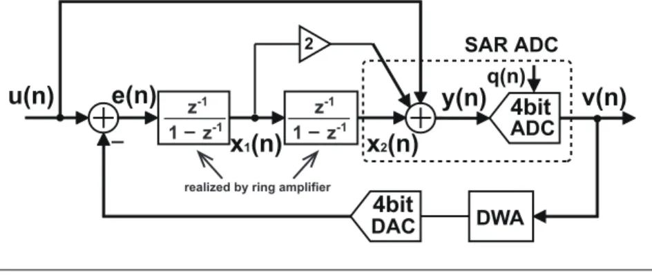
3.1 Block diagram of proposed 2nd-order feed-forward delta sigma mod- ulator with passive-adder embedded SAR quantizer . . . 37
3.2 Circuit implementation of Proposed 2nd-order feed-forward delta sigma modulator using ring amplifier (R-AMP) . . . 38
3.3 Schematic of fully differential R-AMP (Ring-Amplifier) . . . 39
3.4 Integrator using dynamic amplifier consist of inverter . . . 41
3.5 Operation of integrator using dynamic amplifier consist of inverter . . 42
3.6 Track hold circuit using ring amplifier . . . 43
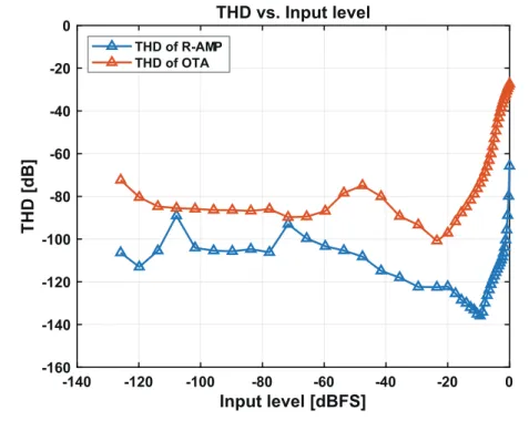
3.7 SNDR & SFDR versus Input level of T/H circuit using ring amplifier and OTA . . . 44
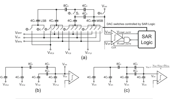
3.8 THD versus Input level of T/H circuit using ring amplifier and OTA . 45 3.9 Implementation of proposed charge redistribution SAR quantizer and it’s the equivalent circuit at two kinds of operation mode . . . 46
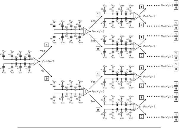
3.10 Switching procedure of proposed 4-bit SAR quantizer . . . 47
3.11 Schematic diagram of dynamic comparator . . . 48
3.12 Schematic diagram of data-weighted-averaging . . . 49
3.13 SPICE simulated results comparison of delta sigma modulator power spectrum at the ON/OFF mode of DWA . . . 50
3.14 Schematic diagram of 1st-stage of ring amplifier for calculating the input-referred thermal noise voltage . . . 52
3.15 Simulated output power spectrum of T/H circuit using ring amplifier 54 3.16 Noise analysis of integrator using ring amplifier . . . 55
3.17 Schematic diagram for the noise analysis simulation of dynamic com- parator using PSS and PNOISE . . . 59
3.18 Circuit implementation for noise analysis of dynamic comparator . . . 60
3.19 Power spectrum of ideal 20-bit SAR quantizer . . . 62
xiii
3.20 Simulated output power spectrum of proposed 2nd-order feed-forward
delta sigma modulator (@Supply voltage = 1.2 V) . . . 63
3.21 Chip microphotograph and layout of the prototype modulator . . . 65
3.22 Measured output power spectrum of proposed 2nd-order feed-forward delta sigma modulator (@Supply voltage = 1.1 V) . . . 66
3.23 Measured SNDR and SNR vs. input signal level . . . 66
3.24 Measured SNDR vs. supply voltage . . . 67
4.1 Block diagram of proposed delta sigma modulator . . . 72
4.2 Simplified circuit implementation of proposed delta sigma modulator 73 4.3 Block diagram of improved delta sigma modulator . . . 74
4.4 Simplified circuit implementation of improved delta sigma modulator 75 4.5 Circuit implementation of proposed 2nd-order feed-forward delta sigma modulator using ring amplifier (R-AMP) with simplified operation phase . . . 77
4.6 Schematic of pseudo differential ring amplifier (R-AMP) . . . 79
4.7 AC analysis circuit of ring amplifier . . . 80
4.8 Open-Loop-Gain of Ring Amplifier versus Amplitude of Output Signal 81 4.9 Circuit Implementation of the improved charge redistribution asyn- chronous SAR quantizer with passive adder . . . 83
4.10 Equivalent circuit of the improved charge redistribution SAR quan- tizer in the different operation. . . 84
4.11 Schematic diagram of asynchronous SAR logic . . . 85
4.12 Schematic diagram of the double-tail dynamic comparator used in SAR quantizer . . . 86
4.13 SPICE simulated results comparison of delta sigma modulator power spectrum at the ON/OFF mode of DWA . . . 88
4.14 Simulated output power spectrum of improved 2nd-order feed-forward delta sigma modulator using dynamic analog component . . . 89
4.15 Chip microphotograph and layout of the prototype modulator . . . 91
4.16 Measured output spectrum for fin ≈26.92kHz and -4dBFS input sig- nal amplitude . . . 92
4.17 Measured SNDR and SNR vs. input signal level . . . 92
5.1 Block diagram of proposed 3rd-order delta sigma modulator using QNS SAR Quantizer . . . 97 5.2 Schematic diagram of proposed 3rd-order feed-forward delta sigma
modulator using ring amplifier (R-AMP) with QNS SAR quantizer . . 98 5.3 Timing chart of proposed 3rd-order feed-forward delta sigma modu-
lator using ring amplifier (R-AMP) with QNS SAR quantizer . . . 99 5.4 Schematic of pseudo differential R-AMP (Ring-Amplifier) . . . 101 5.5 Circuit implementation of proposed passive adder embedded QNS
SAR Quantizer . . . 103 5.6 Schematic diagram of the dynamic comparator used in SAR quantizer 104 5.7 Equivalent circuit of the proposed QNS SAR quantizer in the different
operation . . . 105 5.8 Circuit implementation of proposed the QNS circuit . . . 107 5.9 Equivalent circuits of the five kinds of the QNS circuit’s state . . . 108 5.10 Monte carlo analysis results comparison of delta sigma modulator
performed by matlab with≤1% unit-capacitance random mismatches of DAC . . . 109 5.11 Circuit implementation of the first integrator with DAC . . . 110 5.12 Simulated output spectrum with ≤1% unit-capacitance mismatches
of DAC for fin ≈366.21 kHz and -4.32 dBFS input signal amplitude . . 112 5.13 Power distribution of proposed delta sigma modulator . . . 113
6.1 Radio receiver for wireless communication systems . . . 118 6.2 Block diagram of proposed 6th-order complex bandpass delta sigma
modulator . . . 120 6.3 Schematic diagram of the proposed 6th-Order Complex Bandpass Delta
Sigma AD Modulator with Image Rejection Using Dynamic Amplifier and SAR Quantizer . . . 123 6.4 Clock timing chart of the proposed 6th-Order Complex Bandpass Delta
Sigma AD Modulator with Image Rejection Using Dynamic Amplifier and SAR Quantizer . . . 124
xv
6.5 Block diagram of complex integrator . . . 124
6.6 Schematic diagram of traditional complex integrator . . . 125
6.7 Circuit implementation of the proposed complex integrator . . . 128
6.8 Equivalent circuits of the proposed complex integrator in the four kinds of state . . . 129
6.9 Schematic of pseudo differential ring amplifier . . . 131
6.10 Schematic of RAMP’s core circuit . . . 132
6.11 AC analysis of RAMP (a) Simulation circuit. (b) Frequency character- istics RAMP. . . 133
6.12 Circuit implementation of proposed adder embedded SAR Quantizer with noise coupling in digital domain . . . 135
6.13 Schematic diagram of dynamic comparator used in SAR quantizer . . 136
6.14 Equivalent circuits of proposed adder embedded SAR Quantizer with noise coupling in digital domain . . . 137
6.15 Quadrature DWA logic . . . 138
6.16 Simulated output spectrum with ≤1% unit-capacitance mismatches of DAC for single tone ( fin ≈8.33 MHz with the input signal ampli- tude of -3.25 dBFS) . . . 139
6.17 Simulated output spectrum with ≤1% unit-capacitance mismatches of DAC for double tone ( fin1 ≈8.19 MHz and fin2 ≈8.45 MHz with the input signal amplitude of -9.27 dBFS) . . . 140
7.1 Energy efficiency of ADC . . . 146
7.2 FOMS versus CMOS Technology . . . 148
7.3 FOMW versus CMOS Technology . . . 149
A.1 SQNR of high order delta sigma modulator using 2-bit quantizer . . . 153
A.2 SQNR of high order delta sigma modulator using 3-bit quantizer . . . 154
A.3 SQNR of high order delta sigma modulator using 4-bit quantizer . . . 154
A.4 SQNR of high order delta sigma modulator using 5-bit quantizer . . . 155
A.5 SQNR of high order delta sigma modulator using 6-bit quantizer . . . 155
xvii
List of Tables
3.1 Simulation parameters of delta sigma modulator . . . 63
3.2 Performance summary and comparison with previous works . . . 68
4.1 AC analysis simulation parameters of R-AMP . . . 81
4.2 Simulation parameters of delta sigma modulator . . . 89
4.3 Performance summary and comparison with previous works . . . 93
5.1 Performance summary and comparison with previous works . . . 114
6.1 Performance summary and comparison with previous works . . . 142
xix
List of Abbreviations
DSP Digital Signal Processing ADC Analog-to-Digital Converter
SNDR Signal-to-Noise and Distortion Ratio SoC System on Chip
CMOS Complementary Metal Oxide Semiconductor SAR Successive Approximation Register
OTA Operational Transconductance Amplifier INL Integral-Non-Linearity
LSB Least-Significant-Bit
DAC Digital-to-Analog Converter PSD Power-Spectral-Density FS Full Scale
NTF Noise Transfer Function STF Signal Transfer Function OSR Over Sampling Rate
SQNR Signal-to-Quantization-Noise Ratio ENOB Effective-Number-Of-Bits
DWA Data-Weighted-Averaging
MDAC Multiplying Digital-to-Analog Converter CMFB Common-Mode-Feed Back
SFDR Spurious Free Dynamic Range THD Total Harmonic Distortion MSB Most Significant Bit
PSS Periodic Steady-State analysis PNOISE Periodic Noise analysis RAMP Ring Amplifier
DFF D Flip-Flop
QNS Quantization Noise Shaping CMRR Common Mode Rejection Ratio
CBPDSM Complex Bandpass Delta Sigma Modulator QBPDSM Quadrature Bandpass Delta Sigma Modulator NC Noise Coupling
QDWA Quadrature Data-Weighted-Averaging
xxi
Physical Constants
Boltzmann’s constant k=1.38×10⁻²³J/K
xxiii
List of Symbols
V voltage V
P power W (J s−1)
U sampled input signal E quantization noise
Q shaped quantization noise
T sampling periodic s
S power spectral density f frequency
ω angular frequency rad
γ content associated with CMOS technology
∆ quantization error µ mean value
σ mean-square value
1
Chapter 1
Introduction
1.1 Background
The digital signal processing techniques is performed widely on the computer sys- tems and communication systems. Benefit from digital circuits are robust and can be realized by extremely small and simple structures, the fast, and very complex accu- rate systems can be implemented. As time goes by, the speed and density of digital integrated circuits is increasing, the dominance of digital system in almost all areas of communications system and consumer products is increasingly obvious. How- ever, humans live in the physical world of analog signals, the analog-to-digital data converters (ADCs) are required to interface with the digital signal processing (DSP) system. As the speed and capability of DSP cores increases, the speed and accuracy of the converters associated with DSP have to increases, which led to unprecedented challenges. The performance of ADC is often limited by the available device tech- nology. While recent designs may benefit from scaled device geometries and higher bandwidth, there is a loss in dynamic range and sampling linearity due to reduced supply voltages and available swing.
In recent years, low voltage, high signal-to-noise and distortion ratio (SNDR) ADC analog-to-digital converters are widely used in the mixed-signal system on chip (SoC) in the fields of the wireless sensor network such as human body informa- tion measurement, environmental information monitor, interactive multimedia sys- tem, consumer device and industrial applications. With the feature size of CMOS (Complementary Metal Oxide Semiconductor) devices scaled down, the increasing
16 28 40 65 90 130
180 250
300 350
400
CMOS Technology [nm]
110 120 130 140 150 160 170 180 190
FOMS [dB]
FOMS versus CMOS Technology (1997-2018)
SAR Folding Pipeline Delta-Sigma DT Delta-Sigma CT Flash Two-Step Cyclic
FIGURE1.1: FOMS versus CMOS Technology
16 28 40 65 90 130
180 250
300 350
400
CMOS Technology [nm]
10-1 100 101 102 103 104 105 106
FOMW [fJ/conv-step])
FOMW versus CMOS Technology (1997-2018)
SAR Folding Pipeline Delta Sigma DT Delta Sigma CT Flash Two-Step Cyclic
FIGURE1.2: FOMW versus CMOS Technology
1.1. Background 3
speed of devices has enabled the ADCs to achieve several tens of MS/s to low GS/s sampling rates. However, the degradation of the transistor is influencing the per- formance of integrated circuits, such as the increase of threshold-voltage mismatch, and the reduction of the intrinsic gain. Besides, the dynamic range of analog signal is limited by low supply voltage. Due to the linearity of analog circuit deteriorate, the realization of the high-gain amplifier and high-resolution ADC is difficult. The effects of technology scaling made that to implement accurate, efficient amplifiers is increasingly difficult under the low supply voltage, and the intrinsic properties of transistors were quite different from that of the large size transistor [1].
10 20 30 40 50 60 70 80 90 100 110 120
SNDR @ f in,hf [dB]
10-1 100 101 102 103 104 105 106 107
P/f snyq [pJ]
Energy efficiency of ADC (1997-2018)
SAR Folding Pipeline Delta-Sigma DT Delta-Sigma CT Flash Two-Step Cyclic
FOMW=1fJ/conv-step FOMS=185dB
FIGURE1.3: Energy efficiency of ADC
In order to solve the each scaling challenge, a lot of techniques are proposed as gain enhancement of amplifier, output swing enhancement techniques and many highly effective digital correction. But, the ability of these techniques to deliver favourable amplifier scaling characteristics in actual fabricated designs does not achieve the expectation. As shown in Fig. 1.1 and Fig. 1.2, the ADC performance surveys con- ducted in [2] and[3] show that the high-resolution ADCs implemented in nanoscale CMOS is very few, and its energy efficiency is declining gradually. The Walden FOM
(FOMW) [4] is the respective energy/conversion-step value, it is defined as:
FOMW = P
2×BW×2SNDR−1.76/6.02 [J/conv.−step], (1.1)
where, P is the power consumption of AD convertor, BW is the band width of signal.
The Schreier FOM (FOMS) is the figure of merit that assumes that the ADC power is set by thermal noise, and hence quadruples per 6dB in precision. Schreier originally defined this FOM using DR [5] as:
FOMS= DR+10×log10(BW/P) [dB], (1.2)
where, DR is the dynamic rang of AD convertor. but it has become common to also account for distortion, i.e.
FOMS= SNDR+10×log10(fsnyq/2/P) [dB], (1.3)
where, fsnyq is defined as fsnyq = Sampling-Rate(FS)/Oversampling-rate(OSR) (it is given by 2FS/OSR for a complex delta-sigma modulator), it equal to the double BW.
(e.g. [6]). It is clear from the energy plot shown in Fig. 1.3 that FOMS is a better metric for high-resolution designs. Because, the amplification is used for almost all high resolution ADC circuits, these observations reflect the effect of operation amplifier scaling challenges on the performance of the system level. By contrast, the low and medium resolution ADC architectures which do not use operating amplifier such as SAR (Successive Approximation Register) ADCs can deliver the transistor scaling characteristics very well. SAR ADCs are well known as an energy efficiency architecture for low power, low and medium speed, medium resolution applications [7], [8]. Because the resolution of SAR ADC depends on the accuracy of capacitor matching and the offset of comparator, it is difficult to realize a high resolution SAR ADC in nanoscale CMOS technology. For medium-to-high speed applications, the flash ADC and pipelined ADC have been the popular architectures.
In the most case which the operating amplifier is used, the transistor scaling char- acteristics can not be delivered favourably, since the operation amplifier ill-suited fundamentally to scaling is included in the underlying circuits of ADC. the high
1.1. Background 5
105 106 107 108 109 1010 1011 1012 1013 1014
fsnyq [Hz]
110 120 130 140 150 160 170 180 190
FOMS [dB]
FOMS versus Speed (1997-2018)
SAR Folding Pipeline Delta-Sigma DT Delta-Sigma CT Flash Two-Step Cyclic
FIGURE1.4: FOMS versus Speed
105 106 107 108 109 1010 1011 1012 1013 1014
fsnyq [Hz]
10-1 100 101 102 103 104 105 106
FOMW [fJ/conv-step]
FOMW versus Speed (1997-2018)
SAR Folding Pipeline Delta-Sigma DT Delta-Sigma CT Flash Two-Step Cyclic
FIGURE1.5: FOMW versus Speed
performance operating amplifier in nanoscale technology may be realized by em- ploying the additional techniques, but the ability to scale at the same pace as digital performance improvements can not be achieved. A truly scalable amplifier must be consist of the circuit components which include the characteristics of scaled CMOS.
The technology scaling is deliberately designed to favor the time domain world of high-speed digital, thus the scalable analog techniques will likely be found by using the same method as well. In order to fully exploit the abilities of a transistor, the bias- ing and small signal properties of the device must be viewed as highly coupled, time dependent variables which can be applied as feedback to each other with respect to time [1]. The ring amplification technique is proposed for solving the above prob- lem. The ring amplifier is a small modular amplifier derived from a ring oscillator which naturally embodies all the essential elements of scalability. The ring amplifier not only can realize the amplification with rail-to-rail output swing, but also can effi- ciently charge for the large capacitive loads by using slew-based charging. The ring amplifier is simple enough to be quickly constructed from only capacitors, switches consist of transistors and inverters in series and according to process trends it can be scale well in performance.
On the other hand, since the delta sigma AD modulator reduces the quantization noise in the desired signal band by oversampling and noise shaping technique, it is a digital rich architecture, and it is suitable to realize the high SNDR ADC in nanome- ter CMOS technology as shown in Fig 1.4 and 1.5. Normally, high SNDR modulator is realized by the techniques of high-order noise-shaping and/or higher OSR (Over Sampling Ratio). However, high OSR needs high speed operation and increases the total power consumption of the modulator. High-order noise-shaping needs sev- eral numbers of integrators with power hungry amplifier. Several techniques have been proposed to improve the SNDR and reduce the power consumption of the delta sigma AD modulator. The feed-forward structure is a preferred architecture for delta sigma AD modulator to tolerate the distortion of the internal amplifier [9].
Moreover, the feed-forward structure can also reduce the output swing of the inte- grator, which can relax the linearity requirements on the amplifier in the integrator, and hence to reduce the power consumption of the delta sigma modulator. Multi-bit
1.2. Objectives 7
quantizer can also be chosen to relax the slew-rate requirement on the amplifier to re- duce the power of the modulator [5]. Error feedback technique (noise coupling) also has been proposed to aggressive the noise shaping characteristic of the delta sigma AD modulator [10]. However, in nano CMOS technology, that it is difficult to real- ize a high gain, low distortion, wide band-width amplifier lead to the non-linearity of the amplifier. The variation of the noise transfer function coefficient caused by the non-linearity of the amplifier weakens the delta sigma modulator’s ability for suppressing the in-band quantization noise, thus, the performance of delta sigma modulator is not affected.
1.2 Objectives
IN OUT
CS CC
CF ΦA
ΦA ΦR
ΦR
ΦR
ΦA
High Vth High Vth
Vdd
Vdd
Vdd
High Vth High Vth
MP3
MN3
MP2
MN2
ROS
VOUT
VIN
MP1
MN1
(Example Integrator using ring amplifier)
FIGURE1.6: Implementation of integrator using ring amplifier
In order to achieve the maximum power-efficiency of ADC, the use of the dynamic amplifier (eg. logic inverter or ring amplifier) instead of OTA (Operational Transcon- ductance Amplifier) has been proposed and results in dynamic-analog-components- based Nyquist ADC [11], [12]. Ring amplification is a concept, it can be realized by the variety of architectures and design choices. One such implementation is shown in Fig. 1.6 which embodies the key features of ring amplification. However, there are a lot of implementation approaches available, each with their own pros and cons in terms of operation speed, accuracy, and energy efficiency. Fundamentally, the
ring amplifier is a ring oscillator which is split into two separate signal paths by a resistor or capacitor. A different offset is embedded into each signal path in order to create a range of input values for which neither output transistor nor of Fig. 1.6 (MP3and MN3) will fully conduct. If this non-conduction "dead-zone" is sufficiently large, the ring amplifier will operate by slewing-to, stabilizing, and then locking into the dead-zone region. When placed in the feedback structure which is a example switched capacitor integrator of Fig. 1.6, this charging and settling behavior results in the stabilized waveforms.
the basic characteristics of ring amplifier will be discussed as following, the capacitor CC shown in Fig. 1.6 is used to cancel the difference between the integrator virtual- node sampling reference and the trip-point of the first stage inverter. It ensures that the ideal settled value is independent of the actual inverter threshold. Namely, the generation of operating point depend on the capacitor, rather than the bias current as the traditional amplifier. The input-referred value of offset voltage is negligibly small. The dead-zone of the ring amplifier in Fig. 1.6 is embedded prior to the sec- ond stage inverters by storing a voltage offset across resistor. Any value for within the dead-zone region is a viable steady-state solution for the ring amplifier, and the input-referred value of the dead-zone will determine the overall accuracy of the am- plifier for most practical cases. In other words, the error voltage Verror at when the amplifier has stabilized and locked will be
Verror ≤VDZ/Aamp, (1.4)
where, VDZ is the dead-zone region, Aamp is the final settled small-signal gain of the first stage inverter, and finite gain effects of the latter stages are ignored. It is worth briefly noting that there are many additional options for both where and how to embed the dead-zone offset into the ring amplifier, and for different target accu- racies and design applications it may be useful to consider additional possibilities and their respective advantages and disadvantages. The ring amplifier has several characteristic which is different from the traditional amplifier. The embedding re- sistor allows to accurately and linearly set the dead-zone offset value. Its stability is gained by embedding the offset prior to the second stage inverters, rather than
1.3. Construction 9
the first or third stage. Due to the accuracy limitations imposed by equation 1.4, the input-referred dead-zone value of a few millivolts or less is supposed to achieve the high performance amplification. For medium accuracy ring amplifiers, embedding the dead-zone offsets immediately after the first gain stage will create input-referred dead-zone sizes small enough to achieve desired accuracies while still keeping the embedded offset large enough to easily tune with a simple voltage reference.
Although, the ring amplifier has above superiority, the behaviour of ring amplifier is different from that of the traditional amplifier, the ring amplifier requires to gen- erate the operating point by performing the reset operation before the amplification.
Since the output of ring amplifier is disabled in the process of the reset, the load capacitance must be unconnected to the output of the ring amplifier in the reset op- eration. Furthermore, since SAR quantizer is used as an internal quantizer in the delta sigma modulator, unlike flash ADC, SAR quantizer requires an extra phase for the signal sampling. Because of the above two factors, the clock timing design of delta sigma modulator using SAR quantizer and ring amplifier is more difficult than that of the delta sigma modulator using traditional amplifier and flash ADC.
In this paper, several design technique is proposed for improving the performance of delta sigma modulator using dynamic analog components. The ring amplifier is used for realizing the integrator in the proposed delta sigma modulator. The foible of ring amplifier can be avoided by using the proposed design technique. Benefit from the ring amplifier has the favourable linearity, the in-band noise of the delta sigma modulator can be adequately suppressed. The bias circuit not requited in the ring amplifier, not only the power consumption can be reduced, the energy efficiency of delta sigma modulator can also be improved. Moreover, in the proposed design technique of delta sigma modulator, the SAR quantizer with dynamic comparator is used to realized the internal multi-bit quantizer, which not only can relax the slew- rate requirement on the amplifier but also can improve the energy efficiency of the delta sigma modulator.
Chapter 1: Introlduction (Background, Objectives, Construction) Chapter 2: Theory of Delta Sigma Modulator
Chapter 3: Proposed 2nd-Order Delta Sigma Modulator Using Ring amplifier and Passive Adder Embedded SAR Quantizer
Chapter 4: Proposed 2nd-Order Delta Sigma Modulator Using Ring Amplifier and SAR Quantizer with Simplified Operation Mode
Chapter 5: Proposed 3rd-Order Noise Coupled Delta Sigma Modulator Using Passive Adder Embedded Noise Shaping SAR Quantizer
Chapter 6: Proposed 6th-Order Quadrature Bandpass Delta Sigma Modulator Using Dynamic Amplifier and Noise Coupling SAR Quantizer
Chapter 7: Conclusion
Title: Study on Design Technique of High Resolution ADC Using Dynamic Analog Components
The functional verification of delta sigma modulator using dynamic compinents (ring amplifer)
The operating speed of delta sigma modulator using ring amplifer is enhanced by improving the circuit architecture
The performance of delta sigma modulator using ring amplifer is enhanced by using proposed noise coupling technique
The applications of delta sigma modulator using ring amplifer are expanded by using proposed complex integrator
FIGURE1.7: Construction of this dissertation
1.3 Construction
The construction of this dissertation is shown in Fig. 1.7. It is structured as the fol- lowing: In the chapter 2, The discussion in this section is an introduction to the the- ory of the delta sigma modulator. The oversampling technique, noise shaping tech- nique and the basic architectures of delta sigma modulators are discussed. More- over, the theoretical performance represented by signal to quantization-noise ratio (SQNR) of the high order delta sigma modulator with multi-bit internal quantizer are summarized.
In the chapter 3, a 2nd-order delta sigma modulator using dynamic analog compo- nent is proposed to improve the energy efficiency. The proposed delta sigma mod- ulator is realized by the integrator using the ring amplifier and the passive-adder
1.3. Construction 11
embedded multi-bit SAR quantizer. Because the operating point of ring amplifier is generated by the reset operation dynamically, the current bias circuit is not required.
The passive-adder embedded multi-bit SAR quantizer using dynamic comparator not only realizes the multi-bit quantization, but also realizes an adder for the sum- mation of analog signal without active analog component, since the high energy efficiency can be maintained. Moreover, for conforming the noise characteristic of the dynamic analog components, the noise models of dynamic amplifier (ring am- plifier) and dynamic comparator are created, and these noise analysis are carried out. For demonstrating the proposed techniques, the proof-of-concept prototype of proposed delta sigma modulator using dynamic analog components is designed and fabricated in TSMC 90nm 1P9M CMOS technology. Measurement results show the feasibility of the proposed delta sigma modulator.
In the chapter 4, the drawback of the proposed delta sigma modulator using dy- namic analog components in the chapter 3 is discussed. In order to ensure the ring amplifier’s reset time and that the output operation of the ring amplifier and the sampling operation of asynchronous SAR quantizer are performed at the same time, the 4 operation phases are required for once AD conversion, which limited the oper- ation speed of proposed delta sigma modulator using dynamic analog components.
4 factors need to be guaranteed when designing the delta sigma modulator using ring amplifier and SAR quantizer are summarized for For improving the perfor- mance of proposed 2nd-order delta sigma modulator using dynamic analog compo- nents. Moreover, the 2nd-order delta sigma modulator using dynamic analog com- ponents with simplified operation phase is proposed. The improved delta sigma modulator has been designed and fabricated in 90 nm CMOS technology. Benefit from the reduction of the number of the delta sigma modulator operation phase, the speed of delta sigma modulator is improved. Measurement results show the feasi- bility of the improved delta sigma modulator using dynamic analog components.
In the chapter 5, a 3rd-order delta sigma modulator using ring amplifier and noise shaping SAR quantizer is proposed for enhancing the performance of the delta sigma modulator using dynamic analog components. A novel noise shaping SAR quan- tizer without active components realized in analog domain is proposed to extend
the order of the delta sigma modulator (the signal band width can be extend at the same sampling rate). The proposed passive adder embedded noise shaping SAR quantizer not only can realize the summation of analog signals without the active amplifier, Because a passive adder is embedded to the proposed noise shaping SAR quantizer, the summation of analog signals in front of input port of the internal quantizer can be realized without power hungry amplifier. And, it can also feed the shaped quantizer noise to the loop filter of the delta sigma modulator, which achieve an addition 1st-order noise shaping without the extra integrator. More- over, the pseudo differential ring amplifier with modified common feedback cir- cuit (CMFB) is proposed to improve the common-mode rejection ratio (CMRR). The proposed the modified CMFB circuit does not include capacitors in series, hence, it can directly feed the common mode signal from the output port of the ring ampli- fier’s core to the input port of the ring amplifier’s core for obtaining the maximum CMRR. As a result, the 3rd-order noise coupled delta sigma modulator is realized by two integrators with ring amplifier and the proposed noise shaping SAR quantizer, it achieved the greater bandwidth and the better performance (eg. better FOMW and FOMS) than that of proposed 2nd-order delta sigma modulator using dynamic analog component in previous work. The SPICE simulation results demonstrate the feasibility of the proposed delta sigma modulator in 90 nm CMOS technology.
In the chapter 6, a 6th-order complex quadrature delta sigma modulator (QBPDSM) with 2nd-order image rejection using dynamic amplifier and noise coupling (NC) SAR quantizer embedded by passive adder is proposed for the application of wire- less communication system. A novel implementation of complex integrator circuit is proposed for improving the energy efficiency and reducing the circuit area of QBPDSM. The dynamic amplifier instead of the operational transconductance am- plifier (OTA) is used to achieve the maximum power-efficiency of the operating am- plifier in the complex integrator circuit. The proposed complex integrator circuit requires fewer operation phases than the conventional complex integrator for once
References 13
complex integration operation, hence the energy efficiency can be improved. Fur- thermore, the proposed complex integrator circuit use less capacitance than the con- ventional complex integrator, which can reduce the circuit area of QBPDSM. More- over, the digitized NC SAR quantizer is used for realizing high order noise shap- ing and image rejection for maintaining the high energy efficiency. In the proposed 6th-order QBPDSM, two complex integrators consist of ring amplifiers are used to realize the 2nd-order noise shaping, the passive adder embedded NC SAR quantizer is used to realize the summation of analog signal, quantization, noise shaping and image rejection. SPICE simulation results including the thermal noise and the flicker noise have been done to verify the effectiveness of the proposed architecture and to confirm the performance of the modulator.
In the chapter 7, the conclusion of this dissertation is described.
References
[1] M. Shrivastava et al. “Toward system on chip (SOC) development using FinFet technology: Challenges, solutions, process co-development and optimization guidelines”. In: IEEE Trans. Electron Devices vol.58 (June 2011), pp. 1597–1607 (cit. on pp. 3, 6).
[2] B. Murmann. “ADC Performance Survey 1997-2018”. In: [Online]. Available:
http://web.stanford.edu/ murmann/adcsurvey.html. (2018) (cit. on p. 3).
[3] B. Jonsson. “On CMOS scaling and A/D-converter performance”. In: NORCHIP 2010 (Nov. 2010), pp. 1–4 (cit. on p. 3).
[4] R. H. Walden. “Analog-to-digital converter survey and analysis”. In: IEEE J.
Select. Areas Commun. vol.17 (Apr. 1999), pp. 539–550 (cit. on p. 4).
[5] R. Schreier and G. Temes. Understanding Delta-Sigma Data Converters. Wiley- IEEE Press, 2004 (cit. on pp. 4, 7).
[6] A.M.A. Ali et al. “A 16-bit 250-MS/s IF Sampling Pipelined ADC With Back- ground Calibration”. In: IEEE J. Solid-State Circuits vol.45 (Dec. 2010), pp. 2602–
2612 (cit. on p. 4).
[7] Y.-S Shu, L.-T Kuo, and T.-Y. Lo. “An Oversampling SAR ADC With DAC Mismatch Error Shaping Achieving 105 dB SFDR and 101 dB SNDR Over 1 kHz BW in 55 nm CMOS”. In: IEEE J. Solid-State Circuits vol.51 (Dec. 2016), pp. 2928–2940 (cit. on p. 4).
[8] W. Tseng, W. Lee abd C. Huang, and P. Chiu. “A 12-bit 104 MS/s SAR ADC in 28 nm CMOS for digitally-assisted wireless transmitters”. In: IEEE J. Solid- State Circuits vol.51 (Oct. 2016), pp. 2222–2231 (cit. on p. 4).
[9] J. Silva et al. “Wideband lowdistortion delta-sigma ADC topology”. In: Elec- tronics Letters vol.37 (June 2001), pp. 737–738 (cit. on p. 6).
[10] K. Lee, M.R. Miller, and G.C. Temes. “An 8.1 mW, 82 dB DeltaSigma ADC With 1.9 MHz BW and -98 dB THD”. In: IEEE J. Solid State Circuits vol.44 (Aug.
2009), pp. 2202–2211 (cit. on p. 7).
[11] Y. Chae and G. Han. “Low voltage, low power, inverter-based switched-capacitor delta-sigma modulator”. In: IEEE J. Solid State Circuits vol.44 (Feb. 2009), pp. 458–
472 (cit. on p. 7).
[12] B. Hershberg et al. “Ring amplifiers for switched capacitor circuits”. In: IEEE J. Solid State Circuits vol.47 (Dec. 2012), pp. 2928–2942 (cit. on p. 7).
15
Chapter 2
Theory of Delta Sigma Modulator
2.1 Preface
The discussion in this section is an introduction to the theory of the delta sigma modulator. The oversampling and noise shaping techniques well be discussed. The basic architectures of delta sigma modulators will be presented.
2.1.1 Oversampling
ADC DSP
Amplifier
Analog Domain
Analog input Filter Sensor or Antenna
Interface circuit
(Continuous-time)
Process circuit
(Discrete-time)
Digital Domain
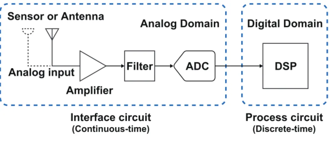
FIGURE2.1: A typical DSP system with interface circuit.
Figure 2.1 shows a typical DSP system that consist of interface circuit and digital signal process circuit. The interface circuit includes the sensor circuit or antenna, amplifier, analog filter and ADC. As shown, the analog input signal is magnified and filtered firstly, then, it is input to ADC and transformed to a digital data stream.
The digital data stream is processed by the DSP circuit. Usually, the ADC can be clas- sified into two main categories, the Nyquist-rate ADC and oversampled ADC. The
Nyquist-rate ADC has some specific property that are a one-to-one correspondence between the input and output samples. The each sampled input signal is separately transformed to the corresponding digital code, regardless of the other sampled in- put signal (Nothing to do with earlier and later input signal); thus, the Nyquist-rate ADC has no memory property. If to apply the digital input word containing bits b1, b2, b3, ..., bN−1, bN of ADC to a ideal DAC, the analog output of ideal DAC can be represented as:
Vout =Vre f × (b12−1+b22−2+b32−4+...+bN−12−(N−1)+bN2−N) +e, (2.1)
where Vre f is the reference voltage, e is the DC offset associated with the imple- mentation of ADC (eg. SAR-ADC is a mid-tread quantizer, Flash-ADC is a mid-rise quantizer, they have a different DC offset value). The conversion resolution of ADC can be evaluated by comparing the actual value of Voutwith the ideal value repre- sented by (2.1).
The sampling rate of Nyquist-rate converter must satisfy the sampling rate required in the Nyquist’s criterion (twice the bandwidth of the input signal). The actual rate is usually somewhat higher than this minimum value required in the Nyquist’s cri- terion. The resolution and linearity of a Nyquist-rate ADC constructed from current sources or switched-capacitor circuit is determined by the matching accuracy of the analog components (eg. resistors, capacitors and transistor) used in the implementa- tion. Thus, the analog components must have a relative matching error less than 2N to guarantee an integral-non-linearity (INT) less than 0.5 least-significant-bit (LSB), it is very difficult to realize the high resolution Nyquist-rate ADC.
However, in some applications such as medical imaging device and digital audio device, higher resolution and linearity is required [1] [2]. The resolution as much as 18 or even 20 bits for ADC is requisite, generally. If the ADC is realized at the Nyquist-rate, then only integrating-ADC or counting-ADC can be used for realiz- ing the capacity such as accuracy above 20 bits. However, the integrating-ADC or counting-ADC require at least 2N clock periods to convert a sampled signal, since,
2.1. Preface 17
they are too slow for most signal-processing applications. The ADC using over- sampling technique are able to achieve over 20 bit resolution at reasonably high conversion speeds by relying on a trade-off. The sampling rate of converter using oversampling technique much higher than the Nyquist-rate, it is typically higher by a factor between 4 and 256, or even higher. The factor is represented as OSR in al- most all literatures. Moreover, the converter using oversampling technique generate each output utilizing all preceding input values. Thus, the converter incorporates memory elements (eg. integrator) in its structure. This property destroys the one-to- one relation between input signal and output signal. Fortunately, in the time domain or in the frequency domain, the comparison of the complete input and output wave- forms can be used to evaluate the resolution of ADC.
2.1.2 Noise Shaping
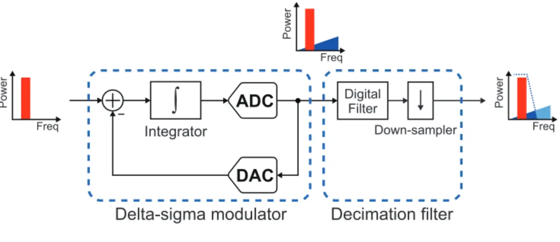
The delta sigma modulator using oversampling technique can realize the high res- olution AD conversion without the high precision analog component. Since it is a digital rich architecture, and have been used widely in the circuit using nanometer CMOS technology.
ADC
DAC
Digital Filter
Delta-sigma modulator
Power
Freq
Power
Freq
Power
Integrator Freq
∫
Down-sampler
Decimation filter
FIGURE2.2: System model of the delta sigma modulator.
Figure 2.2 shows the system model of a first-order delta sigma modulator. It is a feedback loop, containing an internal low-resolution ADC and digital-to-analog con- verter (DAC) as well as a loop filter. As shown, the quantization noise is shifted to the high frequency domain by delta sigma modulator, and then the quantization
noise in the high frequency domain is filtered and down-sampled by the decima- tion filter. Since the quantization noise power in the baseband (i.e. the signal with spectra centred around dc) is reduced, the high SNDR ADC can be realized easily.
However, due to the quantizing effect of the internal ADC and the memorability of the integrator, the delta sigma modulator is a non-linear system. The analysis of the delta sigma modulator is a difficult mathematical task.
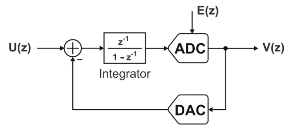
1 - z-1 z-1
ADC
DAC
Integrator
U(z)
E(z)
V(z)
z-1
ADC
DAC
Integrator
U(z)
E(z)
V(z)
Delta Sigma
(a)
(b)
FIGURE2.3: Block diagram of delta sigma modulator. (a) Using dis- crete integrator. (b) Using delay circuit.
Figure 2.3 illustrates a block diagram of basic delta sigma modulator. the block dia- gram of delta sigma modulator using the discrete integrator and the delay circuit are shown in the Figure 2.3(a) and (b), respectively. Where the U(z)is the sampled input signal, the E(z)is the quantization noise of the internal ADC, the V(z)is the output signal of the delta sigma modulator. Figure 2.3 (b) shows the concept of "delta" and
"sigma" that represent what is "delta" and what is "sigma". For analysing the mathe- matical model of the delta sigma modulator, the internal ADC can be represented as a linearized model which consists of a unity-gain amplifier and a quantization noise
2.1. Preface 19
E(z). The DAC is seen as a ideal DAC with the reference voltage of Vre f =1V. By an- alyzing the model of the delta sigma modulator, its output signal can be represented as:
v(n) =u(n) +e(n) −e(n−1), (2.2)
in the time-domain, and,
V(z) =U(z) + (1−z−1)E(z), (2.3)
in the z-domain. The digital output signal includes the analog input signal U(z) and a difference of the quantization between E(z)and its delay z−1E(z). The equa- tion (2.3) means that the analog input signal U(z)is not changed by the delta sigma modulation process, so that, the analog input signal can be recovered by the deci- mation filter without using the integrator in the demodulation operation. Moreover, there are not the amplification of in-band noise and distortion at the delta sigma modulator, the differentiation of the error E(z)suppresses the in-band noise and the distortion. Therefore, the delta sigma modulator has a unity-gain to the input signal U(z)in the signal band, while, the quantization noise is strongly attenuated, this signal process is called as noise shaping in almost all literatures.
The quantization noise and non-linearity of ADC in the delta sigma modulator are shaped, suppressed in the bandwidth. However, due to the non-linearity of DAC in the delta sigma modulator is not any shaped, the output signal and performance of the delta sigma modulator is affected by the DAC. Thus, the non-linearity of DAC is a major limitation that affect the attainable performance of the delta sigma modu- lator. For multi-bit quantization, digital correction or dynamic matching techniques can be used for weakening the influence of the DAC’s non-linearity. Furthermore, there are more simple ways, for example, the single-bit quantization has the char- acteristic of the DAC consists of only two points on its input and output. Since, the single-bit DAC’s operation is inherently linear.
2.2 Mathematical Model of Delta Sigma Modulator
2.2.1 Noise Transfer Function
1 - z-1 z-1
ADC
DAC
Integrator
U(z)
E(z)
V(z)
FIGURE2.4: Block diagram of first-order delta sigma modulator.
Figure 2.4 illustrates a block diagram of the first-order delta sigma modulator. For simplicity, next, the mathematical model of the delta sigma modulator will be dis- cussed by using the model of the first-order delta sigma modulator. The output noise of the first-order delta sigma modulator due to the quantization error of the internal ADC can be represented as:
Q(z) = (1−z−1)E(z), (2.4)
in the z-domain, as shown by (2.3). The the transfer function of the quantization noise (NTF) can be represented as:
NTF(z) = (1−z−1), (2.5)
the z in the equation (2.3) can be replaced by ejω, this becomes
NTF(ejω) = (1−e−jω), (2.6)
where, ω=2π f T, assuming fsas the sampling rate, then, T=1/ fsis the sampling period. Assuming Se(f) as the power-spectral-density (PSD) of the quantization error of the internal ADC of the delta sigma modulator. The PSD of the output noise
2.2. Mathematical Model of Delta Sigma Modulator 21
of the delta sigma modulator can be deduced as:
Sq(f) =NTF(ej2π f T)2Se(f) (2.7)
= (1−e−j2π f T)2Se(f) (2.8)
= ((1−cos(2π f T))2+sin(2π f T)2)Se(f) (2.9)
= (1−2cos(2π f T) +cos(2π f T)2+sin(2π f T)2)Se(f) (2.10)
=2(1−cos(2π f T))Se(f) (2.11)
= (2sin(π f T))2Se(f). (2.12)
The equation (2.12) means that the PSD of the output noise of the delta sigma mod- ulator can be computed by the product of the NTF’s PSD(2sin(π f T))2and the PSD of the internal ADC’s quantization error Se(f).
2.2.2 Quantization Error Model
Next, considering that how to calculate the PSD of the quantization error of the internal ADC. Figure 2.5 illustrates the transfer function diagram of mid-rise and mid-tread quantizer and their quantization error function diagram. The the output of quantizer generates a rise or step when the input of zero is input to the quantizer, as shown in the figure 2.5(a), since it has the characteristic of mid-rise such as SAR ADC. In the figure 2.5(c), the the output of quantizer is a middle of a flat portion i.e.
a tread when the input of zero is input to the quantizer, since it has the characteristic of mid-tread such as Flash-ADC. The step size∆ is set as 2 in figure 2.5(a) and (c) that make the quantization levels of the both types quantizer to be integer values that lead to the difference between input thresholds i.e. the size of LSB equal the∆ (LSB=2). Therefore, in mid-rise quantizer, the quantization levels are odd integers, opposite, the quantization levels are even integers in mid-tread quantizer.
Figures 2.5(b) and (d) illustrate the quantization error function of the mid-rise and mid-tread quantization, respectively. It can be knew from the figures 2.5(b) and (d) that the input and output of the mid-rise quantizer are between -8 and +8, the input and output of mid-tread quantizer are between -9 and +9. The above means,

![Figure 3.11 shows the schematic of a comparator used in SAR quantizer. The dif- dif-ferential output nodes of the dynamic comparator [8] is followed by a NAND gate](https://thumb-ap.123doks.com/thumbv2/123deta/5804953.2045337/72.892.242.702.642.1047/figure-schematic-comparator-quantizer-ferential-dynamic-comparator-followed.webp)
