Charge transfer from CuInS2 quantum dots for
solar cells
著者
? 建?
year
2014
その他のタイトル
太陽電池のためのCuInS2量子ドットからの電荷移動
学位授与大学
筑波大学 (University of Tsukuba)
学位授与年度
2013
報告番号
12102甲第6818号
URL
http://hdl.handle.net/2241/00123308
Charge transfer from CuInS
2
quantum dots for
solar cells
Jianhui SUN
Doctoral Program in Frontier Science
Submitted to the Graduate School of
Pure and Applied Sciences
in Partial Fulfillment of the Requirements
for the Degree of Doctor of Philosophy in
Science
at the
Abstract
The ultrafast carrier dynamics in CuInS2 quantum dots (QDs) was studied by means of
femtosecond transient absorption spectroscopy. The size-dependent 1S transition energy
determined from bleaching spectra is in agreement with that calculated on the
finite-depth-well model in the effective mass approximation. The transient absorption bleaching
comes from filling of electron quantized levels, allowing us to know the dynamics of the 1S
electron in CuInS2 QDs. The sub-100-ps electron trapping at surface defects in bare QDs
accelerates with decreasing the QD size, while is effectively suppressed in well-passivated
CuInS2/ZnS core/shell QDs.
The electron transfer from CuInS2/ZnS core/shell QDs into porous anatase TiO2 films
was studied by time-resolved photoluminescence spectroscopy. The rate and efficiency of
electron transfer can be controlled by changing the core diameter and the shell thickness.
The electron transfer rate reaches 107s−1 for different-sized CuInS
2 core QDs. It is found that the electron transfer rates decrease exponentially at the decay constants of 1.1 and 1.4
nm−1with increasing ZnS shell thickness for core diameters of 2.5 and 4.0 nm, respectively,
in agreement with the electron tunneling model. This shows that optimized electron
transfer efficiency can be realized by controlling the core/shell structures in QDs.
The QDs-sensitized solar cells (QDSSCs) consisting of a TiO2 films co-sensitized with
CuInS2/CdS core/shell QDs and CdS buffer layers was fabricated. The performance
of the QDSSCs assembled with CuInS2/CdS core/shell QDs were superior to those
CuInS2/CdS core/shell QDs was attributed to high efficiency of the electron transfer into
TiO2 films. The high efficiency came from the enhanced delocalization of electron wave
function from core to CdS shell due to lower conduction band offset. Furthermore, the
TiO2 films were coated with the in situ growth of CdS layers by means of successive
ionic layer adsorption and reaction. The CdS layers provides high surface coverage to
prevent interfacial recombination between TiO2 films and electrolyte. Under AM 1.5G
illumination at 100 mW cm−2, the CdS-CuInS2 /CdS core/shell QDs co-sensitized solar
cells exhibited a short-circuit photocurrent (JSC) of 9.3 mA cm−2 , an open-circuit
pho-tovoltage (VOC) of 0.48 V, a fill factor of 0.50 and a power conversion efficiency of 2.27%.
The photocurrent resulting from the CuInS2 QDs is increased because of the CdS coating.
The CdS coating facilitated the separation of photogenerated electrons and holes in the
Contents
1 General introduction 1
2 Synthesis and characterization of CuInS2 quantum dots 9
2.1 Introduction . . . 9
2.2 Synthesis of CuInS2 quantum dots . . . 10
2.2.1 Chemical materials . . . 10
2.2.2 Synthesis procedure . . . 11
2.3 Characterization of CuInS2 quantum dots . . . 12
2.3.1 Optical properties . . . 12
2.3.2 Morphology and crystal structure . . . 14
2.3.3 Electrochemical properties . . . 14
3 Ultrafast carrier dynamics in CuInS2 quantum dots 26 3.1 Introduction . . . 26
3.2 Experimental . . . 27
3.2.1 Sample preparation . . . 27
3.3 Experimental results and discussion . . . 29
3.3.1 Optical nonlinearities in CuInS2 quantum dots . . . 29
3.3.2 Ultrafast carrier dynamics in CuInS2 quantum dots . . . 31
3.4 Conclusions . . . 34
4 Electron transfer from CuInS2 quantum dots to TiO2 films 44 4.1 Introduction . . . 44
4.2 Experimental . . . 45
4.2.1 Sample preparation . . . 45
4.2.2 Time-correlated single photon counting system . . . 47
4.3 Experimental results and discussion . . . 47
4.3.1 Energy levels of CuInS2 quantum dots . . . 47
4.3.2 Electron transfer from CuInS2 quantum dots to TiO2 films . . . 48
4.3.3 Electron tunneling model . . . 50
4.4 Conclusions . . . 52
5 CuInS2 quantum dot sensitized solar cells 62 5.1 Introduction . . . 62
5.2 Experimental . . . 64
5.2.1 Preparation of the photoelectrodes . . . 64
5.2.2 Preparation of the Cu2S counter electrodes . . . 65
5.2.3 Assembly of CuInS2 QDSSCs . . . 66
5.2.4 Characterization . . . 66
5.3 Experimental results and discussion . . . 66
5.3.1 Core/shell QDs sensitized solar cells . . . 66
6 Conclusions 84
Acknowledgements 86
Chapter 1
General introduction
Sunlight is an abundant and renewable energy resource, and converting sunlight into
electricity has been considered as one of the most promising pathway to provide clean
energy. Dye sensitized solar cells (DSSCs) become a promising candidate for offering low
cost solar energy, since they can be fabricated by solution-based processing, such as dip
coating, screen printing, painting and roll-to-roll processing. However, DSSCs are much
less stable so that the devices last less time because of the photo-degradation of the dyes.
Instead of molecular dyes, inorganic quantum dots (QDs) are considered as highly
promising in next-generation solar cells, because QDs have the following advantages:[1–7]
(1) easy tuning of the optical band gap energy by controlling the QD size and composition;
(2) large extinction coefficient, enabling the thickness of the device to be thinner; (3)
higher stability than dyes toward water and oxygen; (4) capacity for generating multiple
excitons from single-photon absorption, through the impact ionization effect, which could
boost the theoretical power conversion efficiency beyond the Shockley-Queisser limit of
33%.[8]
The chalcopyrite-type I-III-VI2 QDs have been proposed because of their less-toxic
FIG. 1.1 Schematic depiction of electron hole pair generation, trapping at surface,
con-version to emitted photons and charge transfer to external electrodes. The competition among them determines the charge separation efficiencies from CuInS2 QDs.
with the optimal spectral range for photovoltaic applications. Furthermore, the band gap
of CuInS2 QDs can be tuned not only by controlling their size[9, 10] and stoichiometry[11, 12]
but also by introducing other elements such as Zn.[13–15] Therefore, they are considered
to be alternative low-toxicity materials as solar harvesters for QDs sensitized solar cells
(QDSSCs).
In QDSSCs, efficient charge transfer from QDs to external electrodes is a key factor
to achieve high power conversion efficiency. The overall charge separation efficiency from
CuInS2 sensitizers, as illustrated in Fig. 1.1, depends on the competitions among photon
emission, charge trapping at surface defects and charge transfer to external electrodes.
in CuInS2 QDs and the way to transfer the photo-generated charges from CuInS2 QDs to
the external electrodes for best performance of the solar cells.
Recently, it had been demonstrated that the radiative recombination in CuInS2 QDs
involves a transition associated with the localized intragap state,[9, 10] since it showed the
long emission-lifetimes as well as the large Stokes-shift between the photoluminescence
(PL) band and the band-edge absorption in CuInS2 QDs. However, the band-edge-carrier
dynamics in CuInS2 QDs is ambiguous, leading to be unable to clarify the origin of the PL
in CuInS2 QDs. It is because the radiative recombination in CuInS2 QDs does not come
from the band-edge transitions. Instead the transient absorption spectra are dominated
by filling of the lowest 1S quantized levels. Therefore, the dynamics of the band-edge
carriers such as the 1S electron trapping at the surface defects can be well resolved in
transient absorption spectra.
In CuInS2-TiO2 donor-acceptor systems, the electron transfer from CuInS2 QDs is
energetically allowable because the lowest unoccupied molecular orbital (LUMO) level of
the porous anatase TiO2films is lower than the LUMO level in bulk CuInS2. From Marcus
theory,[16] the electron transfer rate is determined by the electronic coupling strength
(HDA), the total reorganization energy (λ), and the driving force energy (∆G). In
donor-acceptor hybrid systems of CdSe[17–19], CdS[20], and PbS[21] QDs coupling to TiO2 or
ZnO, the effects of three parameters above on the electron transfer dynamics have been
explored widely. It was reported that both the electron and hole energies as well as the
surface densities increase with decreasing QDs size, which increases the rate of both the
charge transfer and charge trapping at the QD surface in QDs-TiO2 systems. Therefore,
it remains difficult to optimize the overall charge separation efficiency by selectively and
rationally controlling the competing processes in core QDs.
tuned for desired functions. The CuInS2 based semiconductor materials have been
exten-sively tailored and combined into spherical core/shell QDs.[9, 14] By tailoring the potential
energy profile through material choice and degree of quantum confinement via the size and
the shape of the components, the electron and hole wavefunctions in CuInS2 QDs can be
engineered to control the photophysical properties, including energy levels, PL quantum
yield, and the lifetimes of excitons. The CuInS2 QDs have been engineered to exhibit type
I carrier localization by coating ZnS shells and quasi-type II carrier localization by coating
CdS shells.[9] This gives us the opportunities to optimizing the solar energy conversion
by controlling interfacial charge separation processes through wavefunction engineering in
CuInS2 QDs.
Early CuInS2 QDSSCs showed a power conversion efficiency of less than 1%.[22]
Recent-ly, the charge recombination at TiO2/QD/electrolyte interfaces was suppressed by
intro-ducing the buffer layer and the efficiency of CuInS2 QDSSCs were increased to 2.52%.[23–25]
The Teng group further improved the CuInS2 QDSSCs by optimizing the CdS
passiva-tion layer and achieved a power conversion efficiency of 4.2%.[26] The trap states at the
interface or the surface of the QDs play a crucial role in degrading the performance of the
QDSSCs. Although the defects at the interface or the surface of the QDs can be effectively
passivated by CdS or ZnS layers, the actual power conversion efficiency of the QDSSCs
is far below the theoretical value. The origin of such limited performance was ascribed
to the poor charge transfer from CuInS2 QDs to external electrodes. The charge transfer
from CuInS2 QDs is the primary event leading to photocurrent generation in QDSSCs.
As we discussed above, we can optimize the charge transfer process from CuInS2 QDs by
means of wave function engineering in core/shell CuInS2 QDs for best performance of the
CuInS2 QDSSCs.
In this thesis, we have studied the ultrafast carrier dynamics in CuInS2 QDs and the
Fi-nallly, the QDSSCs consisting of a TiO2 films sensitized with CuInS2 QDs was fabricated.
This paper consists of the following chapters. In chapter 2, the synthesis method of
CuInS2 QDs is explained. The ultrafast carrier dynamics in CuInS2 QDs is described
in chapter 3. In chapter 4, the electron transfer process from CuInS2/ZnS core/shell
quantum dots into porous anatase TiO2 films is investigated and written. In chapter
5, the fabrication of the QDSSCs is described and the effect of the band alignment on
Bibliography
[1] W. U. Huynh, J. J. Dittmer and A. P. Alivisatos, Science 295, 2425 (2002).
[2] A. J. Nozik, Phys. E. 14, 115 (2002).
[3] P. V. Kamat, J. Phys. Chem. C. 112, 18737 (2008).
[4] G. Hodes, J. Phys. Chem. C. 112, 17778 (2008).
[5] R. D. Schaller and V. I. Klimov, Phys. Rev. Lett. 92, 186601 (2004).
[6] M. Shalom, I. Hod, Z. Tachan, S. Buhbut, S. Tirosh and A. Zaban, Energy Environ.
Sci. 4, 1874 (2011).
[7] S. H. Im, H. J. Kim, S. W. Kim, S. W. Kim and S. I. Seok, Energy Environ. Sci. 4,
4181 (2011).
[8] S. Shockley and H. J. Queisser, J. Appl. Phys. 32, 510 (1961).
[9] L. Li, A. Pandey, D. J. Werder, B. P. Khanal, J. M. Pietryga, and V. I. Klimov, J.
Am. Chem. Soc. 133, 1176 (2011).
[10] H. Zhong, S. S. Lo, T. Mirkovic, Y. Li, Y. Ding, Y. Li, and G. D. Scholes, ACS Nano.
[11] W. S. Song and H. Yang, Appl. Phys. Lett. 100, 183104 (2012).
[12] B. Chen, H. Zhong, W. Zhang, Z. Tan, Y. Li, C. Yu, T. Zhai, Y. Bando, S. Yang,
and B. Zou, Adv. Funct. Mater. 229, 2081 (2012).
[13] J. Zhang, R. Xie, and W. Yang, Chem. Mater. 23, 3357 (2011).
[14] W. Zhang and X. Zhong, Inorg. Chem. 50, 4065 (2011).
[15] X. Tang, W. Cheng, E. S. G. Choo, and J. Xue, Chem. Commun. 47, 5217
(2011).
[16] R. A. Marcus, J. Chem. Phys. 24, 966 (1956).
[17] K. Tvrdya, P. A. Frantsuzovc, and P. V. Kamat, Proc. Natl. Acad. Sci. 108, 29
(2011).
[18] H. Zhu, N. Song, and T. Lian, J. Am. Chem. Soc. 132, 15038 (2010).
[19] A. Kongkanand, K. Tvrdy, K. Takechi, M. Kuno, and P. V. Kamat, J. Am.Chem.
Soc. 130, 4007 (2008).
[20] D. F, Waton, J. Phys. Chem. Lett. 1, 2299 (2010).
[21] B. R. Hyun, A. C. Bartnik, J. K. Lee, H. Imoto, L. Sun, J. J. Choi, Y. Chujo, T.
Hanrath, C. K. Ober, and F. W. Wise, Nano Lett. 10, 31 (2010).
[22] K. T. Kuo, D. M. Liu, S. Y. Chen and C. C. Lin, J. Mater. Chem. 19, 6780 (2009).
[23] J. Y. Chang, L. F. Su, C. H. Li, C. C. Chang and J. M. Lin, Chem. Commun. 48,
4848 (2012).
[25] T. L. Li, Y. L. Lee and H. S. Teng, J. Mater. Chem. 21, 5089 (2011).
Chapter 2
Synthesis and characterization of
CuInS
2
quantum dots
2.1 Introduction
Cadmium and lead based quantum dots (QDs) have toxicity. Some researchers have
turned their attention to ternary lower toxic I-III-VI2compounds such as CuInS2QDs.[1–14]
The CuInS2 QDs have attracted largest research interest to date among all ternary and
quaternary QDs. In the past few years, a lot of synthesis methods have been developed
for CuInS2 QDs, such as heating-up[1–10] and hot-injection techniques[11–14].
It is known that the key to synthesizing monodisperse ternary QDs is to balance the
reactivity of the two cationic precursors by their ligands, solvent matrix composition,
and reaction temperature. For example, the 1-dodecanethiol can be used to tune the
reactivity of the Cu precursor for synthesis of I-III-VI2 QDs.[1, 5, 6, 9] The 1-dodecanethiol
can simultaneously play a role in stabilizing ligand and the solvent. It can further act as
a sulfur source, because it forms thiolates with various metal salts, and because thiolates
and indium acetate reacted and eventually complexed with 1-dodecanethiol at 180−270◦C yielding CuInS2 QDs in the sub-10 nm range. The exciton Bohr radius in CuInS2 is
around 5 nm and is closed to the size of CuInS2 QDs.[3] The larger QDs can be obtained
by increasing the reaction time. This is probably due to the further decomposition of
1-dodecanethiol. Furthermore, this simple synthetic approach leads to the nearly complete
consumption of the cationic precursors and high reaction yields.
Recently, the noninjection thermal decomposition route had been well developed for
the synthesis of CuInS2 QDs.[1–10] The energy-tunable absorption and emission spectra of
CuInS2QDs was observed. A similar method has also been successfully employed by Li et
al.[1] in the synthesis of CuInS
2 QDs. However, the resulting CuInS2 QDs exhibited poor crystallinity and a large size distribution. In their current work, this synthetic method is
further refined to give high quality monodisperse CuInS2/CdS and CuInS2/ZnS core/shell
QDs in a high quantum yield.[2] The well-developed synthesis of CuInS
2 QDs gives the access to a large variety of theoretical studies, giving further insight into the potential
applications of these QDs.
2.2 Synthesis of CuInS
2quantum dots
2.2.1 Chemical materials
Indium(III) acetate (In(Ac)3, 99.99%), purchased from Sigma-Aldrich
Copper(I) iodide (CuI, 99.5%) purchased from Wako
1-dodecanethiol (DDT, 98%), purchased from Sigma-Aldrich
Zinc stearate (ZnSt2, technical grade), purchased from Sigma-Aldrich
Cadmium oxide (CdO, 99.99%) purchased from Sigma-Aldrich
All chemicals were used as purchased and without further purification.
2.2.2 Synthesis procedure
In a typical synthesis of CuInS2 QDs, 1 m mol indium acetate was mixed with 1 m
mol copper iodide and 10 mL 1-dodecanethiol in a three-necked flask. The mixture was
degassed under vacuum for 5 min and purged with argon for three times. Then the flask
was heated up to 120 ◦C for 20 min until a clear solution was formed. The temperature
was then raised to 230 ◦C and maintained at that temperature for 1−45 min for growth of the different-sized CuInS2 QDs. As the temperature increases, the color of the reaction
solution progressively changed from colorless to green, yellow, red, and finally black,
indicating nucleation and subsequent growth of CuInS2 QDs. At the desired size, the
reaction was quenched by immersing the flask in ice bath. The samples were purified
three times with acetone and finally dispersed into toluene for storage.
Furthermore, the CuInS2 core QDs were coated with shell of ZnS or CdS to form
core/shell QDs by successive ionic layer absorption and reaction (SILAR) methods.[12]
The precursors of Cd and Zn were prepared in advance. The zinc precursor was prepared
by mixing of 2 m mol Zinc stearate and 20 mL 1-dodecanethiol and the mixture was
heated up to 100 ◦C until the solution turned to clear. The cadmium precursor prepared
by a mixing of 2 m mol cadmium oxide, 5 mL 1-oleic acid and 15 mL 1-octadecene and
the mixture was heated up to 255 ◦C under argon until the solution turned to clear.
Then 5 mL crude CuInS2 solution diluted with 5 mL 1-dodecanethiol was loaded in a
three-necked flask. The solution was degassed under vacuum for 5 min and purged with
argon for three times. The solution was heated up to 240 ◦C. The 5 mL zinc precursor
(cadmium precursor) was added dropwise into the reaction solution at 240 ◦C and the
After the shell growth, the reaction was quenched by immersing the flask into ice bath.
The samples were purified three times using hexane/acetone and finally dispersed into
toluene for storage.
2.3 Characterization of CuInS
2quantum dots
2.3.1 Optical properties
Photoluminescence (PL) spectra were recorded by a JASCO F-8500 spectrophotometer.
Steady-state absorption spectra were recorded on a UV-vis-NIR scanning
spectrophotome-ter (Hitachi U-3300). Time resolved PL was measured by means of time-correlated single
photon counting (TCSPC) system coupled to a JASCO CT-25 monochromator and
visi-ble photomultiplier. The samples were excited at 375 nm using a 70 ps pulsed diode lasers
(Hamamatsu PLP-10 ). Time resolution of the TCSPC system was about 1 ns.
It is known that the optical properties of QDs depend on their size, composition and
surface states. The absorption spectra of CuInS2QDs were measured at room temperature
and are shown in Fig. 2.1(a). A broad absorption band for all the samples is observed
together with an absorption tail at long wavelength. Similarly to previous reports,[2, 3]
no sharp absorption peak was observed for any of the samples. The absorption edge
gradually shifts toward longer wavelength with increasing the diameter of the QDs, in
consistent with quantum confinement effect.
The PL spectra of CuInS2 QDs were measured and shown in Fig. 2.1(b). Like previous
reports,[2, 3] the CuInS2 QDs have a very broad PL band with the full width at half
maximum (FWHM) of more than 100 nm. It was observed that the PL band gradually
shifted to the longer wavelength in the NIR range with the increase of the diameters.
not come from excitonic recombination.
After the shell growth, the average diameters of the QDs increased, as was observed in
the transmission electron microscopy (TEM) images in Fig. 2.6. Both optical absorption
and PL spectra of the CuInS2/ZnS core/shell QDs were blue-shifted with respect to those
of their parent CuInS2 QDs, as shown in Fig. 2.2. It is likely indicative of etching
of the core material under shell growth conditions. CdS overgrowth proceeded with a
similar initial blue shift, as shown in Fig. 2.3(a), followed by a subsequent red shift; the
latter is consistent with slight delocalization of the electron into the CdS layer, similarly
to the report of Klimov group.[2] Either ZnS or CdS overcoating results in a dramatic
improvement of the PL quantum yield, as shown in Fig. 2.3(b).
To understand the origin of the PL in CuInS2 QDs deeply, the PL lifetimes of core/shell
QDs were studied by means of time-resolved PL spectroscopy. It is found that the PL
decay curves of as-prepared CuInS2 QDs are multi-exponential in nature. The PL decay
curves are devided into three decay components with the best fit. We attributed the
fast decay time component to be the nonradiative recombination process at the surface
defect states. As shown in Fig. 2.4, the PL lifetimes of the CuInS2/ZnS core/shell
QDs exhibit a significant increase compared with the bare CuInS2 QDs, suggesting the
improved passivation of surface defects in the QDs. Long PL decay components in the
CuInS2 QDs emission band have been previously attributed to surface traps.[3, 4] Our
observation contradicts such an assignment. As shown in Fig. 2.3(a), the PL quantum
yields increased with the improvement of surface passivation by ZnS-shell coating.
Compared to CuInS2/ZnS core/shell QDs, PL lifetimes further increased in CuInS2/CdS
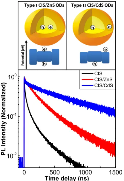
core/shell QDs, as shown in Fig. 2.4. This is because the overlapping of the wave function
for electrons and holes reduces in CuInS2/CdS core/shell QDs. The delocalization of the
Fig. 2.4, the CuInS2 QDs are engineered to exhibit quasi-type II carrier localization by
coating CdS shells.
2.3.2 Morphology and crystal structure
As shown in Fig. 2.5(a-c), the diameters of the three types of CuInS2 core QDs were
determined to be 2.5, 3.3, and 4.0 nm, respectively, by means of TEM. The powder
X-ray diffraction (XRD) patterns shown in Fig. 2.5(e) were obtained from a Rigaku-2000
diffractometer emitting Cu-Kα radiation. The reflection peaks of CuInS2 QDs at 28.5
degree, 47.4 degree, and 55.5 degree in 2θ can be assigned to (112), (220)/(204), and
(312)/(116) planes of a tetragonal chalcopyrite structure of CuInS2, in consistent with
the selected area electron diffraction patterns shown in Fig. 2.5(d).
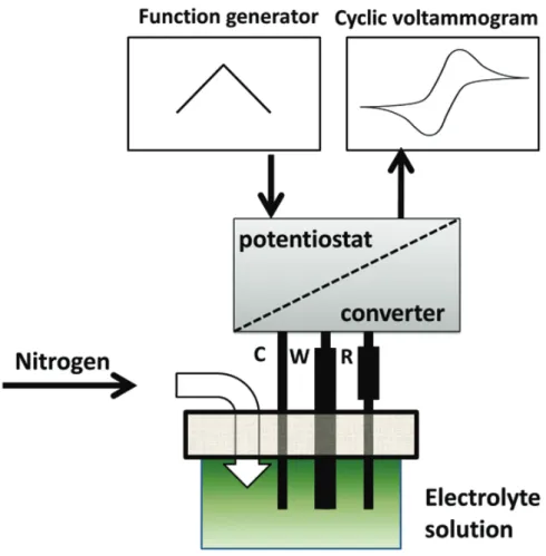
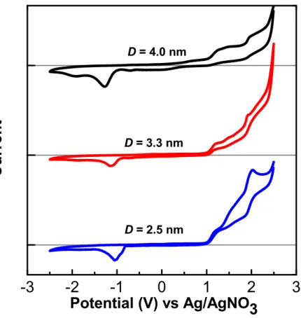
2.3.3 Electrochemical properties
The band gaps and energy levels of the QDs are important parameters for devices
de-sign and material selections in solar cells. Cyclic voltammetry has been proven to be
an effective way to determine the bandgaps and the energy levels of the highest
occu-pied molecular orbital (HOMO) and the lowest unoccuoccu-pied molecular orbital (LUMO) of
QDs.[3, 15] The oxidation process is related to the injection of a hole into the HOMO levels,
and the reduction process is related to the injection of an electron into the LUMO levels.
The energy levels can be calculated from the onset oxidation potential (Eox) and onset
reduction potential (Ered), respectively, according to the following equations
EHOMO = -(Eox + 4.71) eV,
ELUMO = -(Ered + 4.71)eV,
where the unit of the potentials is V vs Ag/Ag+ (0.01 M) reference electrode.
Table 2.1 The LUMO and HOMO levels of CuInS2 QDs. The values of Eg were determined from cyclic voltammograms.
Diameters of CuInS2 QDs (nm) LUMO (eV) HOMO (eV) Eg (eV)
2.5 −3.65 −5.76 2.11
3.3 −3.77 −5.74 1.97
4.0 −3.88 −5.73 1.85
the working electrode (W), a Pt plate as the counter electrode (C), and Ag/Ag+ in 0.1
M tetrabutylammonium hexafluorophosphate (TBAPF6) dissolved in acetonitrile as the
reference electrode (R). TBAPF6 was dissolved in acetonitrile (0.1 M) as the supporting
electrolyte. A drop of the high concentration CuInS2 QDs solution was placed on the
surface of the working electrode and then the solvent was evaporated to form a film of
QDs on the surface of the electrode. After measurement, the glassy carbon disk was first
cleaned in hexane for about 5 min then in acetone for another 5 min and dried before the
deposition of new samples.
The LUMO and HOMO energy levels of the CuInS2 core QDs were obtained from
cyclic voltammetric curves in Fig. 2.8. The resulting energy levels were summarized in
Table 2.1 The energy of the HOMO levels decreases and the energy of the corresponding
LUMO levels increases with the increase of the diameters, in consistent with quantum
Bibliography
[1] L. Li, T. J. Daou, I. Texier, T. Thi, K. Chi, N. Q. Liem and P. Reiss, Chem. Mater.
21, 2422 (2009).
[2] L. Li, A. Pandey, D. J. Werder, B. P. Khanal, J. M. Pietryga, and V. I. Klimov, J.
Am. Chem. Soc. 133, 1176 (2011).
[3] H. Zhong, S. S. Lo, T. Mirkovic, Y. Li, Y. Ding, Y. Li, and G. D. Scholes, ACS Nano.
4, 5253 (2010).
[4] H. Zhong, Y. Zhou, M. Ye, Y. He, J. Ye, C. He, C. Yang and Y. Li, Chem. Mater.
20, 6434 (2008).
[5] W. S. Song and H. Yang, Appl. Phys. Lett. 100, 183104 (2012).
[6] B. Chen, H. Zhong, W. Zhang, Z. Tan, Y. Li, C. Yu, T. Zhai, Y. Bando, S. Yang,
and B. Zou, Adv. Funct. Mater. 22, 2081 (2012).
[7] J. Zhang, R. Xie, and W. Yang, Chem. Mater. 23, 3357 (2011).
[8] W. Zhang and X. Zhong, Inorg. Chem. 50, 4065 (2011).
[10] X.Yuan, J. Zhao, P. Jing, W. Zhang, H. Li, L. Zhang, X. Zhong, and Y. Masumoto,
J. Phys. Chem. C. 116, 11973 (2012).
[11] M. Nam, S. Lee, J. Park, S.-W. Kim and K.-K. Lee, Jpn. J. Appl. Phys. 50, 0602
(2011).
[12] J. Park and S.-W. Kim, J. Mater. Chem. 21, 3745 (2011).
[13] H. Zhong, Z. Wang, E. Bovero, Z. Lu, F. C. J. M. Van Veggel and G. D. Scholes, J.
Phys. Chem. C 115, 12396 (2011).
[14] H. Zhong, Y. Y. Li, M. Ye, Z. Zhu, Y. Zhou and C. Yang, Nanotechnology 18, 025602
(2007).
[15] B. R. Hyun, A. C. Bartnik, J. K. Lee, H. Imoto, L. Sun, J. J. Choi, Y. Chujo, T.
400 500 600 700 800 0.0 0.5 1.0 500 600 700 800 0.0 0.5 1.0 (b) A b s o r b a n c e Wavelength (nm)
Increasing reaction time
(a) 1 min 5 min 10 min 20 min 30 min 45 min
Increasing reaction time 1 min 5 min 10 min 20 min 30 min 45 min P L i n t e n s i t y ( N o r m a l i ze d ) Wavelength (nm)
FIG. 2.1 (a) Absorption and (b) Photoluminescence (PL) spectra of CuInS2 QDs with different reaction time at tempreture of 230 ◦C.
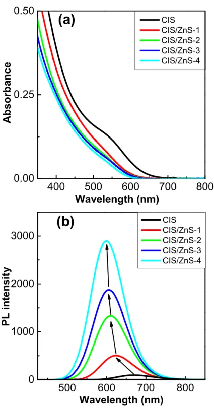
400 500 600 700 800 0.00 0.25 0.50 500 600 700 800 0 1000 2000 3000 (a) CIS CIS/ZnS-1 CIS/ZnS-2 CIS/ZnS-3 CIS/ZnS-4 A b s o r b a n c e Wavelength (nm) (b) CIS CIS/ZnS-1 CIS/ZnS-2 CIS/ZnS-3 CIS/ZnS-4 P L i n t e n s i t y Wavelength (nm)
FIG. 2.2 (a) Absorption and (b) PL spectra of CuInS2/ZnS core/shell QDs with increas-ing the shell thickness.
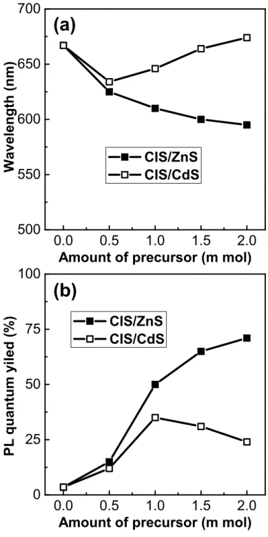
0.0 0.5 1.0 1.5 2.0 500 550 600 650 700 0.0 0.5 1.0 1.5 2.0 0 25 50 75 100 (b) CIS/ZnS CIS/CdS W a v e l e n g t h ( n m )
Amount of precursor (m mol) (a) CIS/ZnS CIS/CdS P L q u a n t u m y i l e d ( % )
Amount of precursor (m mol)
FIG. 2.3 (a) Photoluminescence peaks and (b) quantum yields of CuInS2/ZnS and CuInS2/CdS core/shell QDs as a function of the amount of precursor injected into the reaction.
0 500 1000 1500 10 -2 10 -1 10 0 CIS CIS/ZnS CIS/CdS P L i n t e n s i t y ( N o r m a l i ze d ) Time delay (ns)
FIG. 2.4 Photoluminescence decay curves of the CuInS2 QDs, CuInS2 QDs/ZnS core/shell QDs and CuInS2 QDs/CdS core/shell QDs. The delocalization of the electron wave function from core to CdS shell was enhanced due to the lower conduction band offset between CuInS2 and CdS. The CuInS2 QDs was synthesized to exhibit quasi-type II carrier localization by coating CdS shells.
20 30 40 50 60 70 80 (e) D = 4.0 nm D = 3.3 nm (e) (312)/(116) (220)/(204) I n t e n s i t y ( a . u . ) 2 (Degree) (112) (a) (b) (c) (d) (112) (220)/(204) (312)/(116) D = 2.5 nm
FIG. 2.5 Transmission electron microscopy (TEM) images for CuInS2 QDs (a) 2.5 nm, (b) 3.3 nm and (c) 4.0 nm in diameter; (d) a typical selected area electron diffraction pattern and (e) powder X-ray diffraction patterns of CuInS2 QDs.
D=2.7 0.4 nm 0.3 ML 1.1 ML 2.3 ML 3.2 ML D=3.2 0.3 nm D=3.9 0.5 nm 0 1 2 3 4 5 6 D=4.6 0.7 nm Diameter (nm)
-3 -2 -1 0 1 2 3 D = 4.0 nm D = 3.3 nm D = 2.5 nm C u r r e n t Potential (V) vs Ag/AgNO 3
FIG. 2.8 Cyclic voltammograms of three kinds of CuInS2 QDs 2.8, 3.3 and 4.0 nm in diameter.
Chapter 3
Ultrafast carrier dynamics in CuInS
2
quantum dots
3.1 Introduction
Quantum dots (QDs) exhibit profound size-dependent optical and electronic properties,
having attracted much interests in both fundamental science and applications to solar
cells[1, 2]and light emitting diodes.[3, 4]The carrier relaxation in QDs is extremely sensitive
to the surface characteristics due to the considerable surface-to-volume ratio. The defects
on the QD surface such as the dangling bonds act as the trap states near the band edge.
In most cases, carrier trapping at the surface defects takes place in less than 100 ps in
CdS[5] and CdSe[6–9] QDs. The fast carrier-trapping significantly reduces the efficiency of
the band-edge photoluminescence (PL). As alternatives to II-VI QDs, chalcopyrite-type
I-III-VI2 QDs have been proposed because of their less-toxic components. Among them,
CuInS2 QDs are important candidates for optoelectronic devices, because bulk CuInS2
has a direct band gap of 1.53 eV.[10–13] Naturally, the ultrafast carrier dynamics in CuInS 2 QDs have become of great interest.
Recently, it has been demonstrated that the radiative recombination in CuInS2 QDs
involves a transition associated with the localized intragap state,[10, 12] since it showed
the long emission-lifetimes as well as the large Stokes-shift between the PL band and
the band-edge absorption in CuInS2 QDs. However, the band-edge-carrier localization by
intragap states in CuInS2 QDs is ambiguous, leading to be unable to clarify the origin of
the PL in CuInS2 QDs. It is because the radiative recombination in CuInS2 QDs does not
come from the band-edge transitions. The dynamics of the band-edge carriers can not
be directly resolved in the time-resolved PL spectroscopy.[11, 12] In contrast, the transient
absorption (TA) spectra are dominated by filling of the lowest 1S quantized levels and
the dynamics of the band-edge carriers such as the 1S electron trapping at the surface
defects can be well resolved.
In this chapter, we investigated the mechanisms for optical nonlinearities and ultrafast
carrier dynamics in CuInS2 QDs by means of femtosecond TA spectroscopy. We observed
a nearly symmetrical bleaching band and a broad photoinduced absorption (PA) region
in the TA spectra. Furthermore, we measured the laser-intensity dependence of the TA
to confirm that the band-edge bleach in CuInS2 QDs is dominated by filling of 1S electron
states. From the initial decay of the bleaching, the surface trapping of the 1S electrons
had been studied in CuInS2 core and CuInS2/ZnS core/shell QDs.
3.2 Experimental
3.2.1 Sample preparation
We synthesized the CuInS2 core and CuInS2/ZnS core/shell QDs by a wet chemical
method.[10] The average diameters of three kinds of CuInS
2 QDs were determined to be 2.5, 3.3, and 4.0 nm, respectively, by means of transmission electron microscopy (TEM).
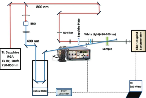
FIG. 3.1 Optical setup of the femtosecond transient absorption (TA) spectrometer.
3.2.2 Femtosecond transient absorption spectrometer
The white-light femtosecond TA spectrometer used in this study is based on a
regen-eratively amplified Ti:sapphire laser system (Spectra-Physics, 800 nm, 130 fs, and 1 kHz
repetition rate). As shown in Fig. 3.1, pump pulses at 400 nm were generated by
fre-quency doubling of the 800 nm laser beam in a BBO crystal 2 mm thick. The white-light
probe was generated by focusing the 800 nm laser beam onto a sapphire plate 2 mm thick.
The pump pulses were chopped by a synchronized chopper to 25 Hz. After the sample,
the probe was focused into a fiber-coupled spectrometer (Ocean Optics USB2000+, 2048
pixel CCD, 300-1100 nm). The angle between pump and probe polarizations was set at
magic angle (54.6 degree) to ensure the dynamics free from reorientation effects. The
group velocity dispersion of the whole experimental system was compensated by a chirp
3.3 Experimental results and discussion
3.3.1 Optical nonlinearities in CuInS
2quantum dots
The steady-state absorption, PL and TA spectra for CuInS2 QDs grown at 230 ◦C are
shown in Fig. 3.2. The absorption edge and PL band gradually shift toward longer
wave-length with increasing the diameter of the QDs, in consistent with quantum confinement
effect. Like previous reports,[10–12] no sharp excitonic absorption peak was observed in the
steady-state absorption spectra. It is well known that the presence of discrete electronic
states is masked in the linear absorption spectra by large inhomogeneous broadening in
CuInS2 QDs.[12, 14] Each QD may vary in size, geometry, and stoichiometry, especially
for CuInS2 QDs because of their ternary chemical-composition. These variations cause a
strong inhomogeneous broadening of the optical transitions. In contrast, the structures of
the 1S transition can be well resolved in nonlinear TA spectra, as shown by dash-dotted
lines in Fig. 3.2. This is because the nonlinear TA spectra are dominated by bleaching of
the 1S transitions after the fast intraband carrier relaxation is completed.
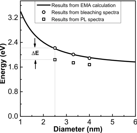
Furthermore, we calculated the band gaps, the lowest optical transition energy of
CuInS2 QDs on the finite-depth-well model in the effective mass approximation. The
effective masses of electrons and holes are 0.16m0 and 1.30m0, respectively, where the m0
is the electron mass in vacuum.[12] As shown in Fig. 3.3, size-dependent 1S transition
energy determined from bleaching spectra is in agreement with that calculated. On the
other hand, the emission peak deviates from its corresponding band gap calculated, and
the deviation, that is Stokes shift, increases up to 0.38 eV with the decrease in the size
of CuInS2 QDs. Besides, it was reported that the radiative recombination in CuInS2
QDs showed the long emission-lifetime of more than 300 ns.[10, 19] This suggests that the
characters of the carrier in CuInS2 QDs. Two features are observed in the TA spectra
presented in Fig. 3.4: a rather symmetrical bleaching band and a broad PA region
extending to low-energy side in the spectra. The bleaching of 1S transitions increases
with the increase of pump fluence. As shown in Fig. 3.5, the bleaching saturated at
higher fluence indicates that the number of states of 1S transitions is finite in CuInS2
QDs. It had been suggested that the band-edge bleach at room temperature is dominated
by filling of 1S electron states without a discernible contribution from holes in CuInS2
QDs.[10] This is because the degeneracy of the valence band is much larger than that of
the conduction band, which is a combined result of the large difference between electron
and hole masses (mh/me= 8) and the multiband structure of the valence band in CuInS2.
When the pump-photon energy (3.1 eV) is much higher than the band gap of QDs
so that the saturation at the pump wavelength is insignificant, the populations in the
QDs following the Poisson distribution: P (N ) =⟨N⟩Ne−⟨N⟩/N ! can be calculated, where P (N ) is the probability of having N electron-hole pairs in a dot in case the average
populations of QDs are ⟨N⟩.[8, 15] The 1S absorption change (∆A) is proportional to the population of the 1S electron state. It can be expressed as ∆A ∝ ⟨n1S⟩, where ⟨n1S⟩ is the average occupation number of the 1S electron state. Because of the twofold spin
degeneracy for the 1S electron state shown in the inset in Fig. 3.5,⟨n1S⟩ can be calculated
as: ⟨n1S⟩ = 1 − e−⟨N⟩(1 +⟨N⟩/2).[15] At the initial stage (∆t = 4 ps) of the 1S electron
relaxation, ⟨N⟩ is directly proportional to the pump fluence (jp) and can be expressed as:
⟨N⟩ = jpσa,[16] in which the σa is the absorption cross section of a QD at the excitation
wavelength of 400 nm.[17] Therefore, we obtain the following expression:[8, 15, 17]
⟨n1S⟩ = 1 − e−jpσa(1 + jpσa/2). (3.1)
As seen in Fig. 3.5, the data show the initial linear growth followed by saturation similarly
to the behavior observed in CdSe QDs.[8, 15] The fitting yields σ
aof 3.9×10⁻¹⁶(cm2), which is comparable to the calculated value of 3.5× 10⁻¹⁶ (cm2) for a 2.5 nm CuInS2 QD at the wavelength of 400 nm.[10] The good fit confirms that the band-edge bleach in CuInS2
QDs is dominated by filling of 1S electron states.
The PA observed in QDs is associated with either the Coulomb multiparticle
in-teractions, such as the biexciton effect[8, 14] or the trapped-carrier related excited-state
absorption[15]. Although the ground biexciton states can be formed in CuInS
2 QDs, the sharp biexcitonic features are not observed probably due to the broadening of the 1S
bleach band. As shown in Fig. 3.4, there is little wavelength selectivity in the spectra
of PA of CuInS2 QDs. Moreover, the PA signals show the linear growth with the pump
fluence and do not show saturation as shown by hollow squares in Fig. 3.5. Therefore,
the spectrally-broad PA observed in CuInS2 QDs most likely originates from the
transi-tion of carriers trapped at defect states. Furthermore, the PA observed in well-passivated
CuInS2/ZnS core/shell QDs indicated that carriers are trapped even inside the CuInS2
QDs, in consistent with the recent report claiming the internal defect states stem from
the substitution of the copper and indium ions in CuInS2 QDs.[10]
3.3.2 Ultrafast carrier dynamics in CuInS
2quantum dots
It is an important concern that a high probability of the carrier trapping at surface
defects degenerates the performance of QD-based optoelectronic devices.[10, 18, 19] It was
found that the low efficiency of the electron injection into TiO2 films from small CuInS2
QDs was attributed to the large amount of surface-localized states.[19] Recently, the
car-rier trapping in CuInS2 QDs has been studied mainly by means of time-resolved PL
spectroscopy.[10–13] These reports show that the luminescence of the CuInS
signif-electron and hole trapping at the trap states in the time-resolved PL spectroscopy,
be-cause both electrons and holes contribute to the PL dynamics.[8] As discussed above, the
TA spectra are dominated by filling of 1S electron states after the intraband relaxation.
Therefore, we can use the 1S bleaching decay dynamics to evaluate the depopulation rate
of the 1S electrons in CuInS2 QDs. The 1S electron relaxation paths in CuInS2 QDs can
be clearly revealed.
For all the decay curves shown in Fig. 3.6, the TA kinetics can not be fitted by a
single-exponential decay. The TA kinetics show two distinct regions: the initial fast decay in
sub-100-ps followed by slow nanosecond decay. A quantitative analysis of the decay curves
was carried out by a simple bi-exponential fit. The initial decay in sub-100-ps as well as
the corresponding signal decrease is sensitive to the size of the CuInS2 QDs. In smallest
CuInS2 QDs, the population of 1S electron decreases quickly at a time constant of 14 ps
by 23% of the initial peak amplitude followed by slow decrease at a time constant of 1.8
ns by 77% of the initial peak amplitude. The TA measurement was performed in the
low-intensity excitation regime (average number of absorbed photons equals to 0.5) where
the fast multiparticle Auger recombination was insignificant.[7, 8] The initial 14 ps decay
is most likely due to the electron relaxation from the 1S state to a new state, such as
the surface-defect state in the band gap. The inset in Fig. 3.6 shows a plot of
initial-decay rate (1/τi) as a function of the average radius (R). The initial-decay rates slow
markedly as the QD radius increases. The solid line in the inset in Fig. 3.6 shows the
best fit of these data by a power-law expression: 1/τi = CRn, where C is a constant and
n describes the order. The fitting yields n of −1.8, which is comparable to the reported
one (−1.5) for CdSe QDs.[20] The electron capture rate at the surface of CuInS 2 QDs was evaluated to explain the relationship between QDs radius and the initial-decay rate.
The details of the calculation were described previously.[19] As shown in the inset in Fig.
follow the size dependence of R−1.6, in reasonable agreement with the size dependence
of the initial-decay rate of R−1.8. The agreement with the calculation indicates that the
initial-decay rate is proportional to the existing probability of electron at the QD surface.
Therefore, the initial decay in sub-100-ps in CuInS2 QDs is due to the electron relaxation
from the 1S state to the surface-defect state.
We further investigated the 1S electron trapping at the defects by making ZnS shells
on CuInS2 core QDs. After overcoating with ZnS, the quantum yield of PL increased
from 3.5% in the core QDs to 81% in the CuInS2/ZnS core/shell QDs. The significant
increase in efficiency of the band-edge PL indicates that the surface defects in bare QDs
are effectively passivated by ZnS shells. As seen in Fig. 3.7, the bleaching in CuInS2/ZnS
core/shell QDs recovers extremely slowly in contrast with the fast recovery of the bleaching
in CuInS2 core QDs. The initial-decay time increased up to 91 ps with a small decay
amplitude of 1.3%. The improvement in surface passivation leads to the suppression of
the fast decay component, confirming that the fast decay component comes from electrons
trapping at surface defects. However, the PA is observed at the lower energy side of the
bleaching band in well-passivated CuInS2/ZnS core/shell QDs, as shown in Fig. 3.8.
The observed PA in CuInS2/ZnS core/shell QDs originates from the transition of carriers
trapped at internal defects. Besides, the 1S bleaching spectra show the red shift (about 10
nm) as the time proceeds in CuInS2 core QDs. This indicates that the different relaxation
behavior is associated with a size inhomogeneity in CuInS2 core QDs. The relaxation of
the 1S electrons is faster in smaller QDs with larger density of electrons at surface.
The PL in CuInS2 QDs had been previously attributed to the recombination of
donor-acceptor pairs.[13]In recombination of donor-acceptor pairs, the electrons and holes at the
band edge are fast trapped by the donors (about 10-20 ps) and the acceptors (within 1
observation contradicts with the previous report which claimed that the PL in CuInS2
QDs comes from the recombination of donor-acceptor pairs. The localized carrier in
CuInS2 QDs must be the hole. The long-lifetime emission is most entirely involved with
the transition from a 1S electron state to a hole-localized state.
3.4 Conclusions
In summary, we have investigated the mechanisms for optical nonlinearities and
ultra-fast carrier dynamics in CuInS2 QDs by means of femtosecond TA spectroscopy. The
size-dependent 1S transition energy was obtained from bleaching spectra in agreement
with the calculated one. From pump-intensity dependence of the TA spectra, we found
that the 1S absorption changes as a function of pump fluence could be well fitted on the
state-filling model. In state-filling model, the population of electrons follows the Poisson
distribution. Therefore, the TA bleaching in CuInS2 QDs is dominated by filling of the 1S
electron states. Based on such a verdict, the ultrafast electron dynamics was investigated
in CuInS2 QDs. The decay in sub-100-ps is due to the electron relaxation from the 1S
state to a surface-defect state. We found that the sub-100-ps electron trapping in bare
QDs accelerated with decreasing QDs size. The rates of the electron trapping were shown
to scale with the inverse of QD radius (1/τi∝ R−1.8). These surface trapping states were effectively passivated in CuInS2/ZnS core/shell QDs. The experimental results clearly
show the intrinsic characters of the 1S electron states in CuInS2 QDs and the way to
Bibliography
[1] W. U. Huynh, J. J. Dittmer, and A. P. Alivisatos, Science 295, 2425 (2002).
[2] I. Gur, N. A. Fromer, M. L. Geier, and A. P. Alivisatos, Science 310, 462 (2005).
[3] S. Coe, W. K. Woo, M. Bawendi, and V. Bulovi´c, Nature 420, 800 (2002).
[4] J. L. Zhao, J. A. Bardecker, A. M. Munro, M. S. Liu, Y. H. Niu, I. K. Ding, J. D.
Luo, B. Q. Chen, A. K.-Y. Jen, and D. S. Ginger, Nano Lett. 6, 463 (2006).
[5] V. I. Klimov, P. H. Bolivar, and H. Kurz, Phys. Rev. B 53, 1463 (1996).
[6] V. I. Klimov and D. W. McBranch, Phys. Rev. Lett. 80, 4028 (1998).
[7] V. I. Klimov, A. A. Mikhailovsky, D. W. McBranch, C. A. Leatherdale, and M. G.
Bawendi, Science 287, 1011 (2000).
[8] V. I. Klimov, J. Phys. Chem. B 104, 6112 (2000).
[9] P. T. Jing, W. Y. Ji, X. Yuan, M. Ikezawa, L. G. Zhang, H. B. Li, J. L. Zhao and Y.
Masumoto, J. Phys. Chem. Lett. 4, 2919 (2013).
[11] X. Yuan, J. L. Zhao, P. T. Jing, W. Zhang, H. B. Li, L.G. Zhang, X. H. Zhong and
Y. Masumoto, J. Phys. Chem. C. 116, 11973 (2012).
[12] H. Zhong, S. S. Lo, T. Mirkovic, Y. Li, Y. Ding, Y. Li, and G. D. Scholes, ACS Nano.
4, 5253 (2010).
[13] B. Chen, H. Zhong, W. Zhang, Z. Tan, Y. Li, C. Yu, T. Zhai, Y. Bando, S. Yang
and B. Zou, Adv. Funct. Mater. 22, 2081 (2012).
[14] V. I. Klimov, S. Hunsche, and H. Kurz, Phys. Rev. B 50, 8110 (1994).
[15] Semiconductor and Metal Nanocrystals: Synthesis and Electronic and Optical
Prop-erties, ed. by V. I. Klimov, Dekker, New York, (2004).
[16] The pump fluence (jp) is presented in terms of the number of photons per cm2.
[17] J. Nanda, S. A. Ivanov, H. Htoon, I. Bezel, A. Piryatinski, S. Tretiak, and V. I.
Klimov, J. Appl. Phys. 99, 034309 (2006).
[18] K. Dohnalov´a, A. N. Poddubny; A. A. Prokofiev, A. M. W. D. de Boer; C. P. Umesh;
J. M. J. Paulusse, H. Zuilhof, and T. Gregorkiewicz, Light: Sci. Appl. 2, e47 (2013).
[19] J. H. Sun, J. L. Zhao, and Y. Masumoto, Appl. Phys. Lett. 102, 053119 (2013).
[20] S. L. Sewall, R. R. Cooney, K. E. H. Anderson, E. A. Dias, D. M. Sagar, and P.
400 500 600 700 800 P L i n t e n s i t y ( N o r m a l i ze d ) A a n d A ( N o r m a l i ze d ) CIS/ZnS QDs D = 2.5 nm D = 3.3 nm Wavelength (nm) D = 4.0 nm
FIG. 3.2 Steady-state absorption (A) (dashed lines), photoluminescence (PL) spectra
(solid lines) and TA spectra (dash-dotted lines) of CuInS2 QDs with three average diam-eters. Steady-state absorption (circles), PL spectra (triangles) and TA spectra (squares) of CuInS2/ZnS core/shell QDs with core diameters of 2.5 nm. By the peak values ∆A and PL normalized. The absorption is normalized at 450 nm. For TA measurement, the pump fluence is set to ⟨N0⟩ = 0.5 for each sample (average number of absorbed photons equals to 0.5) at wavelength of 400 nm and pump-probe delay time is 4 ps.
1 2 3 4 5 6 0.0 0.8 1.6 2.4 3.2
Results from EMA calculation Results from bleaching spectra Results from PL spectra
E E n e r g y ( e V ) Diameter (nm)
FIG. 3.3 The size-dependent 1S transitions determined from bleaching spectra is
illus-trated by circles and size-dependent energy levels of PL are illusillus-trated by squares. The solid line represents the calculated band gaps as a function of the diameters of CuInS2 QDs on the finite-depth-well model in the effective mass approximation (EMA).
0.36 mJ/cm 2 0.72 mJ/cm 2 0.90 mJ/cm 2 2.15 mJ/cm 2 3.58 mJ/cm 2 500 550 600 650 700 -30 -20 -10 0 10 t = 4 ps (a) A Wavelength (nm)
FIG. 3.4 Transient absorption spectra of CuInS2 QDs 2.5 nm in diameter recorded at five pump fluencies.
550 nm 680 nm 0 2 4 6 8 10 -20 -10 0 10 20 30 40 1D N = 2 1P A Pump fluence (mJ/cm 2 ) (b) 1S 40 10 -3
FIG. 3.5 The bleach amplitude of CuInS2 QDs at the 1S absorption peak as a function of the pump fluence. Pump-probe delay time is 4 ps and the solid line is the best fit by Eq. (3.1) in the text.
0 100 200 300 400 500 10 -1 10 0 1.0 1.5 2.0 2.5 0.00 0.05 0.10 22 ps 14 ps D = 2.5 nm D = 3.3 nm D = 4.0 nm A ( N o r m a l i ze d ) Time delay (ps) Probe at 1S transition 35 ps i ( p s -1 ) Radius (nm)
FIG. 3.6 The normalized TA kinetics of CuInS2 QDs with three diameters. The rates of the electron trapping are plotted in the inset by hollow squares. The solid line in the inset shows the fit by a power-law expression. The calculated electron densities at the QD surface as a function of radius are shown by a dashed line in the inset. The electron densities were normalized to the slowest measured-trapping-rate for comparison. For TA measurement, the pump fluence is set to ⟨N0⟩ = 0.5 for each sample (average number of absorbed photons equals to 0.5) at wavelength of 400 nm.
0.8 ps 10 ps 105 ps 505 ps 1005 ps -8 -6 -4 -2 0 2 500 550 600 650 -15 -10 -5 0 (a) CIS QDs 2 10 -3 (b) 0.8 ps 10 ps 105 ps 505 ps 1005 ps CIS/ZnS QDs A Wavelength (nm)
FIG. 3.7 Transient absorption spectra of (a) CuInS2 QDs and (b) CuInS2/ZnS QDs in toluene. The pump fluence is set to ⟨N0⟩ = 0.5 for each sample (average number of absorbed photons equals to 0.5) at wavelength of 400 nm.
0 100 200 300 400 500 10 -1 10 0 0 20 40 0.0 0.5 1.0 CIS QDs CIS/ZnS QDs A ( N o r m a l i z e d ) Time delay (ps) Time delay (ps) A ( N o r m a l i z e d )
FIG. 3.8 The normalized TA kinetics of CuInS2 QDs and CuInS2/ZnS core/shell QDs. The inset shows the enlarged TA kinetics in a short time scale. The probe wavelengths for CuInS2 and CuInS2/ZnS core/shell QDs are 550 and 530 nm, respectively. For TA measurement, the pump fluence is set to ⟨N0⟩ = 0.5 for each sample (average number of absorbed photons equals to 0.5) at wavelength of 400 nm.
Chapter 4
Electron transfer from CuInS
2
quantum dots to TiO
2
films
4.1 Introduction
Quantum dots (QDs) have been considered as a revolutionizing material in
next-generation photovoltaics (PVs)[1, 2] because of their size-dependent properties, flexible
solution-processing, and higher photostability compared to traditional organic dyes.
Ef-ficient electron transfer (ET) from QDs to external electrodes is a key factor to achieve
high power-conversion-efficiency in PVs. From Marcus theory,[3] the ET rate is
deter-mined by the electronic coupling strength (HDA), the total reorganization energy (λ),
and the driving force energy (∆G). In donor-acceptor hybrid systems of CdSe,[4–6] CdS[7]
and PbS QDs[8] tethered to TiO
2 or ZnO, the effects of above three parameters on the ET dynamics have been explored widely. The photoelectrochemical response has been
tuned via the size control of CdSe QDs to obtain the maximum photoconversion
efficien-cy in QD-sensitized solar cells.[6] It is well known that overcoating CdSe QDs with wide
enhance their photo- and thermal-stability[9] and efficiency[10]in QD-sensitized solar cells.
Bulk CuInS2 has a direct bandgap of 1.53 eV, which is well matched with the optimal
spectral range for photovoltaic applications, resulting in Cd-free solar harvesters in solar
cells. The band gap of CuInS2 QDs can be tuned not only by controlling their size[11, 12]
and stoichiometry[13, 14], but also by introducing other elements such as Zn[15–18].
There-fore, they are considered to be alternative low-toxicity materials as solar harvesters for
the solution-processed PVs.[19] We need to fully understand the extraction efficiency of
photogenerated charges from CuInS2 QDs to the external electrodes, such as TiO2, by
controlling their size and surface structures for better performances of the PVs.
In this chapter, we demonstrated efficient electron injection from CuInS2 core and
CuInS2/ZnS core/shell QDs to the porous anatase TiO2 films by using steady-state and
time-resolved photoluminescence (PL) spectroscopy. The relevant energy levels of CuInS2
QDs are obtained by cyclic voltammetry (CV) measurements, which is in accordance
with the values calculated by the effective mass approximation (EMA).[12] The lowest
unoccupied molecular orbital (LUMO) level in CuInS2 QDs is above that of the TiO2
films, resulting in the efficient electron injection into TiO2 films from CuInS2 QDs. The
effect of the core diameter and the ZnS shell thickness on the ET rate and efficiency is
studied in detail. We make the tunneling calculation to describe the ET rate as a function
of the shell thickness and to understand the ET rate and efficiency in the QD/TiO2system.
4.2 Experimental
4.2.1 Sample preparation
The CuInS2 core and CuInS2/ZnS core/shell QDs were synthesized by means of the
FIG. 4.1 Optical setup of the time-correlated single photon counting system.
CuInS2 core QDs to be 2.5, 3.3, and 4.0 nm, respectively. Furthermore, the CuInS2 core
QDs were coated with a ZnS shell to form the CuInS2/ZnS core/shell QDs by means of
a successive ionic layer adsorption and reaction (SILAR) methods.[13] The size and the
size distribution histogram of the CuInS2/ZnS core/shell QDs determined by TEM are
shown in Fig. 2.6. The TiO2 and ZrO2 metallic oxide electrodes used in this work were
fabricated by the same method reported by Heimer et al.[20] As for the QDs-sensitization,
metallic oxide electrodes were tethered 3-mercaptopropionic acid (MPA) first and then
4.2.2 Time-correlated single photon counting system
Time-resolved PL was measured by means of a time-correlated single photon counting
(TCSPC) system with a visible photomultiplier and a 70 ps picosecond pulsed diode laser
emitting at 375 nm. Time resolution of the TCSPC system was about 1 ns.
4.3 Experimental results and discussion
4.3.1 Energy levels of CuInS
2quantum dots
The absorption and PL spectra of synthesized CuInS2 core QDs are shown in Fig. 4.2.
The absorption edge gradually shifts toward longer wavelength with increasing the
diame-ter of the QDs, in consistent with quantum confinement effect. Emission peaks of the QDs
exhibit a large Stokes shift of about 300 meV from their corresponding optical band gaps,
indicating that the radiative transition does not come from excitonic recombination.[11–14]
The LUMO and the highest occupied molecular orbital (HOMO) energy levels of the
CuInS2 core QDs were obtained from a CV method. The resulting energy levels shown
in Fig. 4.3 by red circles are consistent with the energy levels calculated in EMA with
a finite-depth well,[12] where LUMO and HOMO levels of bulk CuInS2 are assumed to
be -4.1 eV and -5.6 eV,[21] respectively. The effective masses of electrons and holes are
0.16m0 and 1.30m0, respectively, where the m0 is the electron mass in vacuum.[10] The
LUMO level of the porous anatase TiO2 film obtained from the CV method is located at
-4.21 eV, which is much lower than the LUMO level of -3.88 eV for the largest CuInS2core
QDs. Therefore, the ET from the QDs to the porous anatase TiO2 films is energetically
allowable. According to the Marcus theory, the ET between two states is dominated by
∆G.[3, 4] In the case of electron injection into TiO
2, the ∆G is the difference between the lowest quantum electron level of the QDs and the LUMO level of TiO . As the
Table 4.1 The efficiency (ηET) and the rate (κET) of electron transfer (ET) from CuInS2 QDs to the porous anatase TiO2 film.
Diameters of CuInS2 QDs (nm) κET (107s−1) ηET (%)
2.5 6.0 69
3.3 5.4 74
4.0 4.5 83
∆G between acceptor and donor systems increases, the ET rate increases and reaches a
maximum when the ∆G is equal to the reorganization energy.
4.3.2 Electron transfer from CuInS
2quantum dots to TiO
2films
In Fig. 4.4, PL decay curves of the CuInS2 core QDs 2.5, 3.3, and 4.0 nm in average
diameter deposited on TiO2 and ZrO2 films are shown. From the PL dynamics of the
CuInS2 core QDs, the fast decay comes from nonradiative surface-traps and the slow
decay comes from radiative recombination emission. Recently, the long lifetime emission
was suggested to originate from the recombination from an electron quantum state to
a localized hole state.[11] The LUMO level of the ZrO
2 film was obtained to be −3.17 eV, which is even higher than the LUMO level of -3.65 eV in the smallest CuInS2 core
QDs. Therefore, the ET from CuInS2 QDs to ZrO2 is energetically unfavorable, and thus
the observed PL decay curves in this system can be used as a reference. The significant
shortening in the PL decays of CuInS2 core QDs is clearly observed. This suggests that
the ET adds another decay channel to the excited states of the QDs. To calculate the
ET rate, we assume that the average PL lifetimes of the QDs on TiO2 and ZrO2 films are
given by τQD−TiO2 = 1/(kR+ kNR+ kET) and τQD−ZrO2 = 1/(kR+ kNR), respectively, where
kR and kNR are radiative and nonradiative decay rates for QDs, respectively.[4–6] The ET
rate (kET) and efficiency (ηET) can be calculated as: kET = 1/τQD−TiO2 − 1/τQD−ZrO2 and
summarized in Table 1. The ET rate reaches 107 s−1 close to the rate in CdSe-TiO
2 donor-accepter systems.[4, 6, 23] The rate slightly increases with decreasing the core diameters of
the CuInS2 QDs, in consistent with the Marcus theory. However, the size dependence of
the ET rate is clearly lower than that of CdSe QDs.[4]On the other hand, the ET efficiency
shows the opposite trend. The maximum efficiency is obtained in the largest CuInS2 QDs.
It has been reported the ET process is impeded in QDs by the considerable amount of
surface-localized trap states.[1, 5] Considering that the luminescence of the CuInS 2 QDs is significantly reduced by the surface traps and that the PL lifetimes of CuInS2 QDs in
toluene are shortened with decreasing the diameters, we attribute the low ET efficiency
in small CuInS2 QDs to the relatively large amount of surface-localized states.
As is known, the stability of bare QDs remains an issue due to photo-induced
oxida-tion in photovoltaic devices.[5] We further investigated photoinduced ET into TiO 2 from CuInS2/ZnS core/shell QDs. With increasing the ZnS shell thickness, the PL peak of
the QDs slightly shifts to higher energy compared with the bare QDs, which is slightly
different from the case of CdSe/ZnS core/shell QDs.[11, 13]For CuInS2/ZnS core/shell
QD-s, the surface coating by a ZnS shell involves an interdiffusion alloying procesQD-s, perhaps
resulting in formation of an inner alloying layer and etching of the CuInS2cores. However,
we ignored the size change of the CuInS2 core in order to facilitate the estimation of the
ZnS shell thickness. As shown in Fig. 4.5, the PL lifetimes of the CuInS2/ZnS core/shell
QDs tethered onto the ZrO2 films exhibit a significant increase with increasing the shell
thickness, suggesting the improved passivation of surface defects in the QDs.
In Fig. 4.5, PL decay curves of the two series of CuInS2/ZnS core/shell QDs 2.5 and
4.0 nm in core diameter tethered onto the TiO2 films are shown. It is expected that the
ZnS shell acts as a tunneling barrier for ET from the photoexited CuInS2 QDs to the
plotted as a function of ZnS shell thickness are shown in Fig. 4.6. As we expected, the ET
rate rapidly decreases with increasing the ZnS shell thickness. The decrease in the ET rate
is considered to result from the weak electronic coupling between the TiO2 films and the
QDs with the increase of the ZnS shell thickness. Surprisingly, the ET efficiency slightly
decreases with the increase of ZnS shell thickness. For example, the ET efficiency of QDs
2.5 nm in core diameter decreases from 65% for the 1.1 monolayer (ML) ZnS shell to
38% for the 3.2 ML ZnS shell. Despite the significant decrease in the ET rate in contrast
with that for the CuInS2 core QDs, the CuInS2/ZnS core/shell QDs exhibit only a slight
reduction in ET efficiency with increasing the ZnS shell thickness. This is because a thin
ZnS shell can effectively reduce the number of the traps as nonradiative recombination
centers and results in efficient enhancement in the PL quantum efficiency.[11] This gives
us a hint that how we can control the ET rate and the ET efficiency in such a
donor-accepter system by controlling the QDs shell thickness to optimize the performance of the
QD-based solar cells.
4.3.3 Electron tunneling model
We assume the LUMO and HOMO levels of the CuInS2 core remain unchanged for
different thickness of the ZnS shell and ignore the intersphere distance between the
CuInS2/ZnS QDs and TiO2 films.[23] The ET rates should be related to the thickness
of the shell and could be described by the following expression:[5, 22]
k(d) = k0e−βd , (4.1)
where d is the thickness of the ZnS shell, k0 is the ET rate for bare QDs. Experimental
plots of the two series of ET rates as a function of ZnS shell thickness can be well fitted by
barrier shell. The fitting by the equation (4.1) yields semilogarithmic slopes, β, of 1.1 and
1.4 nm−1 for CuInS2/ZnS core/shell QDs 2.5 and 4.0 nm in core diameter, respectively.
The slope is comparable to reported one (3.5 nm−1) for CdSe QDs.[5] The value of β for
2.5 nm QDs is less than that in the 4.0 nm QDs. This is because β is dependent on
the barrier height for the 1S electron in the CuInS2 core to tunnel into the ZnS shell.
Therefore, the 1S electron in the small CuInS2 core is easier to tunnel into the ZnS shell
than that in the large core, resulting in smaller factor β.
The eigen function and energy of the electron in CuInS2/ZnS core/shell QDs were
calculated to quantify the effect of ZnS shell thickness on the ET rate by modeling them
as a particle confined in a spherical well of finite depth.[24, 25]The effective mass of electrons
is 0.28m0 for ZnS.[5] The LUMO levels are -4.1 eV for the CuInS2 core, -3.1 eV for the
ZnS shell[5] and -0.4 eV for the MPA, as shown in Fig. 4.7.[26] To intuitively illustrate
the radial distribution of the wave function for the 1S electron, we performed a potential
well calculation in spherical symmetry for CuInS2/ZnS core/shell QDs with a 4 ML ZnS
shell, as shown in Fig. 4.7. The electron wave functions spread into the ZnS shell and
their amplitudes decrease exponentially with increasing the shell thickness. We performed
the calculation for the CuInS2/ZnS core/shell QDs having the same core and ZnS shells
differently thick. The diameter of the CuInS2 core was chosen to be 2.5 and 4.0 nm
based on TEM images. As shown in Fig. 4.6, the calculated radial electron densities
at the ZnS surface as a function of the ZnS shell thickness are in reasonable agreement
with the experimental plots of the shell-thickness-dependent ET rates for the two series
of CuInS2/ZnS core/shell QDs. The good agreement with the theoretical calculation
confirms the tunneling of the electron through the ZnS barrier shell. On the other hand,
this result suggests that optimizing ET efficiency can be realized by controlling the density
4.4 Conclusions
In summary, we have investigated the ET process from CuInS2 core and CuInS2/ZnS
core/shell QDs to the porous anatase TiO2film. The ET rate reaches 107 s−1 for
different-sized CuInS2 core QDs. The ET rate as a function of shell thickness was well expressed
by an exponential function for the core/shell QDs with core diameters of 2.5 nm and 4.0
nm. This trend is well explained by the electron tunneling calculation of the core/shell
QDs. The ET rate is proportional to the existing probability of electrons at the QD
surface decreasing exponentially with increasing the shell thickness. These results show
the possible ways of optimizing the ET efficiency and QD stability by controlling the core
Bibliography
[1] W. U. Huynh, J. J. Dittmer, and A. P. Alivisatos, Science 295, 2425 (2002).
[2] I. Gur, N. A. Fromer, M. L. Geier, and A. P. Alivisatos, Science 310, 462 (2005).
[3] R. A. Marcus, J. Chem. Phys. 24, 966 (1956).
[4] K. Tvrdya, P. A. Frantsuzovc, and P. V. Kamat, Proc. Natl. Acad. Sci. 108, 29
(2011).
[5] H. Zhu, N. Song, and T. Lian, J. Am. Chem. Soc. 132, 15038 (2010).
[6] A. Kongkanand, K. Tvrdy, K. Takechi, M. Kuno, and P. V. Kamat, J. Am.Chem.
Soc. 130, 4007 (2008).
[7] D. F, Waton, J. Phys. Chem. Lett. 1, 2299 (2010).
[8] B. R. Hyun, A. C. Bartnik, J. K. Lee, H. Imoto, L. Sun, J. J. Choi, Y. Chujo, T.
Hanrath, C. K. Ober, and F. W. Wise, Nano Lett. 10, 31 (2010).
[9] J. B. Sambur and B. A Parkinson, J. Am. Chem. Soc. 132, 2130 (2010).