Japan Advanced Institute of Science and Technology
JAIST Repository
https://dspace.jaist.ac.jp/Title
Defect termination on crystalline silicon surfaces by hydrogen for improvement in the passivation quality of catalytic chemical vapor-deposited SiN_x and SiN_x/P catalytic-doped layers
Author(s) Thi, Trinh Cham; Koyama, Koichi; Ohdaira, Keisuke; Matsumura, Hideki
Citation Japanese Journal of Applied Physics, 55(2S): 02BF09-1-02BF09-6
Issue Date 2016-01-22
Type Journal Article
Text version author
URL http://hdl.handle.net/10119/13833
Rights
This is the author's version of the work. It is posted here by permission of The Japan Society of Applied Physics. Copyright (C) 2016 The Japan Society of Applied Physics. Trinh Cham Thi, Koichi Koyama, Keisuke Ohdaira, and Hideki Matsumura, Japanese Journal of Applied Physics, 55(2S), 2016, 02BF09-1-02BF09-6.
http://dx.doi.org/10.7567/JJAP.55.02BF09 Description
1
Defect termination on crystalline silicon surfaces by hydrogen for improvement in the passivation quality of catalytic chemical vapor-deposited SiNx and SiNx/P
catalytic-doped layers
Trinh Cham Thi1,2,†, Koichi Koyama1,2, Keisuke Ohdaira1,2,*, and Hideki Matsumura1,2
1
Japan Advanced Institute of Science and Technology (JAIST),
Nomi, Ishikawa 923-1292, Japan
2
CREST, Japan Science and Technology Agency (JST),
Kawaguchi, Saitama 332-0012, Japan
E-mail: [email protected]
We investigate the role of hydrogen (H) in the improvement in the passivation quality of silicon nitride (SiNx) prepared by catalytic chemical vapor deposition (Cat-CVD) and Cat-CVD SiNx/phosphorus (P) Cat-doped layers on crystalline silicon (c-Si) by annealing. Both structures show promising passivation capabilities for c-Si with extremely low surface recombination velocity (SRV) on n-type c-Si. Defect termination by H is evaluated on the basis of defect density (Nd) determined by electron spin
resonance (ESR) spectroscopy and interface state density (Dit) calculated by the Terman
method. The two parameters are found to be drastically decreased by annealing after SiNx deposition. The calculated average Dit at midgap (Dit-average) is 2.2×10¹¹ eV-1cm-2
2
3.1×10¹¹ eV-1cm-2 for the SiNx/c-Si sample with a SRV of 5 cm/s after annealing. The
results indicate that H atoms play a critical role in the reduction in Dit for SiNx/c-Si and
SiNx/P Cat-doped c-Si, resulting in a drastic reduction in SRV by annealing.
†
Present address: Graduate School of Engineering, Nagoya University, Nagoya 464-8603, Japan
3
1. Introduction
Passivation layers for crystalline silicon (c-Si) have recently been the focus of much attention owing to their important contribution to the improvement in c-Si solar cell efficiency by the reduction in electrical loss caused by defects at the c-Si surface. Besides high passivation quality, passivation films with high transparency and antireflective properties are more preferable. Silicon nitride (SiNx), amorphous silicon (a-Si), Al2O3, SiO2, and their stacked layers are excellent passivation layers that
demonstrate outstanding passivation quality [1-7]. The passivation of these layers relies on defect termination and/or field-effect passivation. Regarding the defect termination mechanism, the surface recombination of minority carriers is suppressed by the reduction in interface state density (Dit), whereas minority carrier recombination
probability is decreased by band bending in field-effect passivation. It has been reported that Al2O3 films prepared by atomic layer deposition show low surface recombination velocities (SRVs) of 2 and 6 cm/s on 1.9 Ωcm floating zone (FZ) n-type c-Si and 1.5 Ωcm FZ p-type c-Si, respectively [4]. However, Al2O3 films do not exhibit antireflective properties on c-Si owing to the mismatch of refractive index. SiO2 has high passivation quality, and a low SRV of 2.4 cm/s can be obtained for c-Si passivated with SiO2 films formed by thermal oxidation [3]. However, thermal oxidation requires a high temperature (>1000 oC), which is not suitable particularly for the fabrication of
silicon heterojunction solar cells containing a-Si films with low thermal tolerance. Among these passivation layers, stoichiometric SiNx films with a refractive index of ~2 is the most promising passivation layer because they show not only excellent passivation quality and high transparency but also significant antireflective properties on c-Si. Moreover, the preparation of SiNx films does not require a high temperature. A
4
conventional method used to fabricate SiNx films is plasma-enhanced chemical vapor deposition (PECVD). PECVD SiNx films with high passivation quality having SRVs of
2-10 cm/s have been reported [4,5,7]. The passivation mechanism of PECVD SiNx layers is mainly based on field-effect passivation originating from positive fixed charges in the SiNx films, whereas thermally grown SiO2 layers can significantly reduce Dit.
Typical values of Dit and fixed charge density (Qf) are ~1010 eV-1cm-2 and ~1010 cm-2 for
SiO2 and ~1011 eV-1cm-2 and ~1011 cm-2 for PECVD SiNx layers, respectively [8]. Ion
bombardment during PECVD tends to deteriorate film/interface quality, and if this problem can be solved, SiNx films with higher passivation quality will be realized.
Catalytic CVD (Cat-CVD), often also referred to as hot-wire CVD, is one of the potential methods to overcome the drawback of PECVD [9,10]. Radical species are formed by the decomposition of source gas molecules on a heated catalyzing wire in Cat-CVD. c-Si surfaces are thus not exposed to energetic ions, and good film/c-Si interface properties can be realized. Moreover, the H content of Cat-CVD films is lower than that of PECVD films, resulting in higher stability against light exposure [10]. The Cat-CVD system can also be utilized to form ultrathin doping layers by exposing c-Si surfaces to radicals formed by the decomposition of PH3 or B2H6 radicals [11-15]. This
doping technique, catalytic doping (Cat-doping), can be applied to the improvement in passivation quality since the thin doping layers formed act as field-effect passivation layers. Single Cat-CVD SiNx and Cat-CVD SiNx/phosphorus (P) Cat-doped layer structures can be promising candidates as passivation layers for c-Si. In our previous studies, extremely low SRVmax values of 5 and 2 cm/s have been demonstrated for
n-type c-Si passivated with Cat-CVD SiNx and Cat-CVD SiNx/P Cat-doped layer structures, respectively [13,16]. The SiNx films used in this study have been confirmed
5
to have high transparency and good antireflective properties [16]. It should be emphasized that these extremely low SRVmax values can be obtained only after
postannealing at an appropriate temperature [13,16]. For a Cat-CVD SiNx/c-Si sample, the significant reduction in SRV by postannealing is supposed to be due to defect termination by hydrogen atoms. For a sample with a P Cat-doped layer, the drastic reduction in SRV is probably due to field-effect passivation induced by P donors and defect termination by H during annealing.
In this study, to quantitatively clarify the role of H in the defect termination effect on the passivation of c-Si surfaces, we focus on the following topics: the etching effect of H atoms on c-Si surfaces during the deposition process, H distribution in the films, defect density (Nd) in SiNx films, and Dit at CVD SiNx/c-Si and SiNx/P
Cat-doped c-Si interfaces. The results show that Nd and Dit at midgap (Dit-average) decrease
significantly after annealing. Dit-average drastically decreases from 2×10¹² to 3×10¹¹ eV
-1
cm-2 after annealing. For a sample with a P Cat-doped layer, Dit-average also effectively
decreases from 2×10¹² to 2×10¹¹ eV-1cm-2 after annealing. The results obtained indicate
that H atoms terminate dangling bonds at film/c-Si interfaces. The slightly smaller D it-average for the sample with a P Cat-doped layer may be the contribution of H atoms in a P
Cat-doped layer.
2. Experimental procedure
To clarify the effect of H on the passivation mechanism, we firstly examined the effect of etching by H atoms on c-Si surfaces during SiNx deposition. A 290-µm-thick
n-type (100) FZ Si wafer with a resistivity of 2.5 Ωcm was cleaned in 5% hydrofluoric acid (HF) diluted with deionized (DI) water for 10 s to remove native oxides. The
6
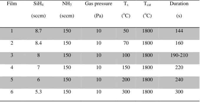
sample was then passivated with SiNx films deposited by Cat-CVD under conditions shown in Table I. After that, the SiNx films were removed in 30% HF diluted with DI
water for 5 s. The complete removal of the SiNx films was confirmed using the Cauchy model of a spectroscopic ellipsometer (J. A. Woollam WVASE32) for data analysis [17]. Surface morphology was then observed by atomic force microscopy (AFM). The surface morphology of bare c-Si after dipping in 30% HF for 5 s was also measured for comparison. For this measurement, two SiNx deposition conditions were selected.
Under one condition, a SiNx film was deposited at a substrate temperature (Ts) of 100 oC,
at which the most significant improvement in the passivation quality of SiNx by annealing is achieved. Under the other condition, SiNx films were deposited at a Ts of
300 oC, at which the highest effective minority carrier lifetime (τeff) is obtained for an
as-deposited sample. The surface morphology of the samples was observed immediately after dipping in DI water and drying with a N2 gun. H distribution is one of the important factors considered to investigate the passivation mechanism of H in SiNx films. In this study, the H profiles in SiNx films before and after annealing at 350 oC for
30 min were measured by secondary ion mass spectrometry (SIMS). We evaluated Nd
using five 2.5×20 mm2 quartz glass substrates with 100-nm-thick SiNx films for each
substrate (500 nm in total) by electron spin resonance (ESR) spectroscopy (JEOL JES-FA100) at room temperature. For τeff measurement, both surfaces of 290-µm-thick
n-type (100) FZ Si wafers with a resistivity of 2.5 Ωcm were passivated with SiNx layers. We carried out microwave photoconductivity decay (μ-PCD) measurement (KOBELCO LTA-1510EP) using a pulse laser with a wavelength of 904 nm and a photon density of 5×1013 cm-2. τeff is expressed as
7 W S bulk eff 2 1 1 ,
where τbulk, W, and S represent the minority carrier lifetime in c-Si bulk, wafer thickness,
and SRV, respectively. In this study, we calculated the maximum SRV (SRVmax) by
assuming τbulk=∞.
In order to accurately confirm defect termination by H atoms on c-Si surfaces, we calculated Dit from the high-frequency experimental capacitance-voltage (C-V) curves
obtained from metal-insulator-semiconductor (MIS) structures by the Terman method [18,19]. A cross-sectional schematic view of the MIS structure is shown in Fig. 1. The experimental preparation for the sample structure has been described elsewhere [16]. The deposition conditions of SiNx films are the same as in Ref. 16 and are summarized in Table I. For a sample with P Cat doping, we used the same condition as that under which we obtained the best SRV after annealing, as reported in Ref. 13. The P Cat doping conditions are summarized in Table II. The samples were annealed three times. The first annealing was conducted after P doping at 400 oC for 30 min, and the second
annealing was conducted after SiNx film deposition at 350 oC for 30 min. An Al ohmic
contact is formed on the back side of the samples by evaporation and annealing at 400 o
C for 10 min. Finally, the front Al electrode was evaporated. A SiNx/P Cat-doped
layer/c-Si sample for lifetime measurement was also prepared and annealed by the same procedure to confirm high passivation quality. The Terman method is mainly based on the comparison of the shapes of the theoretical C-V curve and experimental high-frequency C-V curve. In this study, a high high-frequency of 1 MHz was used for C-V measurement. C-V curves were measured using a Keithley 6517A electrometer/high resistance meter and a 6440B component analyzer. The theoretical curve was calculated
8
using the equations shown in Ref. 18. Dit as a function of surface potential is calculated
using the following equation [19]:
q C d V V d D i s l theoretica g measured g it _ _ ,where Vg is the applied voltage, Ci is the insulator capacitance, q is the elementary
charge, and ψs is the surface potential.
3. Results and discussion
3.1. H etching during SiNx deposition
Cat-CVD is a well-known method, which causes no plasma-induced damage to the substrate surface. However, the substrate surface may be etched by H atoms when it is exposed to a high density of H atoms at a Ts lower than 150 oC [20]. In our study, the
lowest SRVmax of 5 cm/s was achieved for c-Si passivated with SiNx films deposited at a
Ts of 100 oC after annealing. All the samples showed high SRVmax values (≥30 cm/s)
before annealing [16]. One possible reason is supposed to be H etching during SiNx
deposition. However, since the SiNx deposition rate of ~30 nm/min at a Ts of 100 oC is
sufficiently high, the rapid coverage of the c-Si surface by SiNx may suppress the effect
of H etching. To obtain experimental evidence for this speculation, we investigated the effect of H etching during SiNx film deposition by evaluating the surface morphology of c-Si after the deposition and removal of SiNx films. We firstly deposited SiNx films on
the c-Si surface and then examined the surface morphology of the sample after removing the SiNx films using HF solution. The thickness and refractive index of the
9
all by spectroscopic ellipsometry after HF dipping. This observation indicates that SiNx was completely removed from c-Si surfaces.
Figure 2 shows the AFM images of c-Si surfaces after the removal of the SiNx films. The morphology of the c-Si surface without SiNx deposition after dipping in HF is also shown for comparison. For the sample without SiNx film deposition, the
root-mean-square roughness (Rrms) of the c-Si surface is 0.095 nm, whereas those of the
samples with SiNx deposition at Ts values of 100 and 300 oC are 0.13 and 0.10 nm,
respectively. The Rrms of the bare c-Si surface dipped in HF solution is comparable to
those of the samples without HF etching, as reported in Ref. 13. This suggests that the c-Si surface does not deteriorate after dipping in 30% HF for 5 s. The slightly higher
Rrms values obtained for the samples with SiNx deposition and removal indicate that
etching occurs during SiNx deposition. The Rrms of the sample with a SiNx film
deposited at 300 oC is lower than that of the sample with a SiNx film deposited at 100
o
C. H etching during SiNx film deposition might therefore be a possible reason for the higher τeff of an as-deposited SiNx/c-Si structure with SiNx deposited at a higher Ts.
However, since a low SRVmax of 5 cm/s is obtained for the SiNx/c-Si structure with SiNx
films deposited at a Ts of 100 oC, the effect of etching by atomic hydrogen during SiNx
deposition on passivation quality may be negligible.
3.2. H distributions in SiNx films before and after annealing
The improvement in the passivation quality of SiNx films by annealing has been reported by many groups [21-23]. The H distribution in SiNx films is one of the key
10
annealing. The distribution of H atoms inside SiNx films can provide information on H diffusion or release to the environment during annealing, which may lead to the profound understanding of the H defect termination mechanism. In our previous report, H content was calculated from Fourier-transform infrared (FT-IR) spectra using the Lanford method [16, 24]. We found that the Si-H bonding peak signal intensity slightly increases after annealing. The integrated intensity of the Si-H bonding peak signal increases by ~10% after annealing, whereas no change in that of the N-H bonding peak signal is observed. This suggests that H atoms terminate the Si dangling bond inside c-Si and also at the c-SiNx/c-c-Si interface during annealing. We also supposed that H atoms diffuse into the SiNx/c-Si interface, and that more dangling bonds are terminated during
annealing [16].
Figure 3 shows the SIMS profiles of H concentration in SiNx films deposited at a
Ts of 100 oC before and after annealing at 350 oC for 30 min. The H concentration is
constant with the depth of SiNx films. One can see in Fig. 3 that there is no significant difference in H concentration between the samples before and after annealing. Note that the H concentration calculated from the FT-IR spectra of the samples is based on Si-H and N-H bonds in SiNx films. The integrated intensity of the Si-H bonding peak signal
increases when the SiNx films are annealed at 350 oC. The SIMS profiles suggest that
not diffusion but bonding rearrangement during annealing contributes to defect termination, resulting in the improvement in passivation quality. A possible mechanism is that H atoms exiting in voids inside SiNx and at the SiNx/c-Si interface recombine with neighboring Si dangling bonds. In order to confirm defect termination by annealing, in the next subsection, we will report on Nd in SiNx films and Dit at the SiNx/c-Si
11
3.3. Nd in SiNx films and Dit at SiNx/c-Si interfaces
Si dangling bonds back-bonded to three N atoms, N3≡Si∙, generally called K centers, are the main dangling bonds in SiNx films. A K center has three states: K0, K-,
and K+ [25-32]. K+ is the origin of fixed charges in SiNx films and is easily determined
by the negative shift of C-V curves [29-32]. K0 is a dangling bond containing an
unpaired electron and is observable by ESR spectroscopy [25-28]. We have reported that both K0, corresponding to Nd, and K+, corresponding to Qf, decrease markedly after
annealing [16]. In particular, for a SiNx film deposited at a Ts of 100 oC, Qf decreases
from 1×10¹² to 7×1011 cm-2 and Nd decreases from 2×10¹⁸ to 4×1017 cm-3 after annealing.
Figure 4 shows the ESR spectra of SiNx films deposited at various Ts values before and
after annealing at 350 oC for 30 min. The g values obtained were 2.0033-2.0047 for
SiNx films deposited at various Ts values, and the films deposited at lower Ts values
resulted in higher g values. The g reported for the K0 defects is 2.003 [25], and that for
Si dangling bonds in a-Si is 2.0055 [33]. The g value of SiNx films must thus depend on
the chemical composition of the films. The g values obtained in this study may imply that the SiNx films formed are slightly Si-rich, particularly for those formed at lower Ts
values. This is reasonable because the SiNx films are formed so that their refractive indices become 2 and the films formed at lower Ts values have lower densities. From
Fig. 4, one can see that the intensities of dangling bond peak signals decrease greatly after annealing. This is clear evidence of defect termination by H in SiNx films during annealing. This result implies that H can terminate defects not only inside SiNx but also
12
on a SiNx/c-Si interface during annealing, which can lead to a drastic reduction in
SRVmax after annealing.
To demonstrate more clearly the effect of defect termination by H atoms at the interface of a SiNx/c-Si structure, we estimated the Dit of these samples from their C-V
curves by the Terman method. Figure 5 shows the experimental and theoretical C-V curves of the MIS structures with SiNx films deposited at a Ts of 100 °C before and after
annealing. The theoretical C-V curves are drawn under the assumption of no Dit.
Because positive fixed charges exist in SiNx films, the experimental C-V curves were negatively shifted. In the figures, we positively shifted the experimental C-V curves by the flat band voltage values to see clearly the difference between the theoretical and experimental C-V curves. One can see that there is a marked difference in shape between the theoretical and experimental C-V curves of the samples before annealing, whereas a good fitting of the theoretical and experimental curves is obtained for the samples after annealing. This result implies that the samples have higher Dit values
before annealing than after annealing. According to the results of analysis by the Terman method, the Dit values of the samples before annealing are on the order of 1012
eV-1cm-2, whereas those of the samples after annealing are on the order of 1011 eV-1cm-2.
Figure 6 shows the Dit values of SiNx/c-Si structures as a function of surface potential
for SiNx samples deposited at Ts values of 70 and 100 oC before and after annealing. A
significant decrease in Dit-average is observed for the samples after annealing. This
observation is consistent with the improvement in passivation quality and the resulting reduction in SRV. In particular, in the case of the sample deposited at 100 oC, which
demonstrates a low SRVmax of 5 cm/s after annealing, the experimental and ideal C-V
13
Figure 7 shows the SRVmax values of the SiNx/c-Si samples deposited at various Ts
values before and after annealing at 350 oC for 30 min as a function of Dit-average. For the
samples before annealing with large SRVmax values, the Dit-average values are on the order
of 1012 eV-1cm-2. Dit-average decreases to the order of 1011 eV-1cm-2 after annealing, by
which a SRVmax lower than 10 cm/s can be obtained. We suppose that the SRVs of the
samples after annealing are strongly affected by Dit_average rather than by Qf; thus,
SRVmax increases linearly with Dit-average. On the other hand, the samples before
annealing have higher Qf and Dit_average, and both of the two parameters contribute
greatly to the passivation mechanism. The linear tendency of SRV against Dit_average
could thus not be obtained for the samples before annealing. The drastic decrease in Dit
after annealing strongly supports the speculation that H atoms terminate defects at a SiNx/c-Si interface. The calculated result in our study is in good agreement with
previous reports on PECVD SiNx films [8,29,34,35]. Wan et al. reported the Dit of
PECVD SiNx/c-Si interfaces estimated by the Terman method [34]. From their report,
SRVmax becomes less than 10 cm/s when Dit is on the order of 1010 eV-1cm-2 and Qf
~1011 cm-2. SRVmax >100 cm/s corresponds to Dit >1012 eV-1cm-2 and Qf ~ 1012 cm-2.
These are consistent with Dit and SRVmax obtained in our study. Our Cat-CVD SiNx
films have Qf >1011 cm-2 even after annealing. The passivation quality of SiNx films on
c-Si depends on not only Dit but also Qf. A Qf of 7×1011 cm-2 and a Dit of 3.1×10¹¹ eV
-1
cm-2 are typical values for the lowest SRVmax obtained for c-Si passivated with
Cat-CVD SiNx films.
14
As reported previously, P Cat doping contributes significantly to the improvement in the passivation quality of SiNx/c-Si structures. A significantly low
SRVmax of 2 cm/s has been achieved for a SiNx/P Cat-doped c-Si structure after
annealing [13]. The drastic reduction in SRVmax is supposed to be mainly due to the field
effect passivation induced by P donors. The P doping process is conducted at a low Ts
of 80 oC and the sample surface is exposed to a large number of H atoms, and H etching
may occur. Etching can increase surface area, generate more dangling bonds, and/or cause insufficient film coverage on the c-Si surface. On the other hand, H inside the P Cat-doped layer may terminate dangling bonds at the interface of SiNx/P Cat-doped c-Si and contribute to the reduction in SRV during annealing.
Figure 8 shows the Dit values of SiNx/P Cat-doped c-Si and SiNx/c-Si samples
after annealing at 350 oC for 30 min. The Dit-average of the SiNx/P Cat-doped c-Si sample
is 2.0×10¹² eV-1cm-2 before annealing, whereas it decreases to 2.1×10¹¹ eV-1cm-2 after
annealing. Those values are equivalent to those of the SiNx/c-Si sample. We can thus assume that H atoms in a SiNx film contribute greatly to defect termination on a c-Si
surface even in the case of samples with P Cat-doped layers. The reason for the slightly smaller Dit of the SiNx/P Cat-doped c-Si sample than that of the SiNx/c-Si sample might
be the effect of H atoms contained in a P Cat-doped layer. Taken together, we can conclude that both field effect passivation and H defect termination contribute significantly to the improvement in the passivation quality of SiNx/P Cat-doped c-Si structures.
15
H atoms play an important role in the reduction in SRV for both SiNx/P Cat-doped c-Si and SiNx/c-Si samples. Although the c-Si surface is damaged slightly by H etching
during P Cat doping and film deposition, H atoms inside SiNx films can terminate a large number of defects at SiNx/c-Si interfaces during annealing, resulting in the marked improvement in film passivation quality. Dit-average drastically decreases from 2×10¹² to
3×10¹¹ eV-1cm-2 after annealing in the SiNx/c-Si structure. For the sample with a P
Cat-doped layer, Dit-average is also effectively reduced from 2×10¹² to 2×10¹¹ eV-1cm-2 by
annealing. The low Dit-average obtained indicates the good interface quality of Cat-CVD
film/c-Si. The results obtained also demonstrate that H atoms play an important role in the improvement in the passivation quality of SiNx/c-Si and SiNx/P Cat-doped c-Si
structures.
Acknowledgement
16
References
[1] R. Hezel and K. Jaeger, J. Electrochem. Soc. 136, 518 (1989).
[2] A. Focsa, A. Slaoui, H. Charifi, J. P. Stocquert, and S. Roques, Mater. Sci. Eng. B
159-160, 242 (2009).
[3] M. J. Kerr and A. Cuevas, Semicond. Sci. Technol. 17, 35 (2002).
[4] B. Hoex, J. Schmidt, P. Pohl, M. C. M. van de Sanden, and W. M. M. Kessels, J. Appl. Phys. 104, 044903 (2008).
[5] J. Schmidt and M. Kerr, Sol. Energy Mater. Sol. Cells 65, 585 (2001).
[6] Y. Larionova, V. Mertens, N. Harder, and R. Brendel, Appl. Phys. Lett. 96, 32105 (2010).
[7] S. Duttagupta, B. Hoex, and A. G. Aberle, presented at 22nd Int. Photovoltaic Science and Engineering Conf., 2012.
[8] S. W. Glunz, Adv. OptoElectron. 2007, 2 (2007). [9] H. Matsumura, J. Appl. Phys. 65, 4396 (1989). [10] R. E. I. Schropp, ECS Trans. 25, 3 (2009)
[11] H. Matsumura, M. Miyamoto, K. Koyama, and K. Ohdaira, Sol. Energy Mater. Sol. Cells 95, 797 (2011).
[12] T. Hayakawa, Y. Nakashima, M. Miyamoto, K. Koyama, K. Ohdaira, and H. Matsumura, Jpn. J. Appl. Phys. 50, 121301 (2011).
[13] T. C. Thi, K. Koyama, K. Ohdaira, and H. Matsumura, J. Appl. Phys. 116, 114502 (2014).
[14] H. Matsumura, T. Hayakawa, T. Ohta, Y. Nakashima, M. Miyamoto, T. C. Thi, K. Koyama, and K. Ohdaira, J. Appl. Phys. 116, 044510 (2014).
17 (2015).
[16] T. C. Thi, K. Koyama, K. Ohdaira, and H. Matsumura, Jpn. J. Appl. Phys. 53, 022301 (2014).
[17] Guide to Using WVASE32TM: Software for Vase and M-44 Ellipsometers (J. A. Woollam, Lincoln, NE, 1989) p. 159.
[18] E. H. Nicollian and J. R. Brews, MOS Physics and Technology (Wiley, New York, 1982) 3rd ed., pp. 99 and 325.
[19] D. K. Schroder, Semiconductor Device and Characterization (Wiley, New York, 2006) p. 351.
[20] H. Matsumura, K. Kamesaki, A. Masuda, and A. Izumi,Jpn. J. Appl. Phys. 40, L289 (2001).
[21] B. Sopori, R. Reedy, K. Jones, Y. Yan, and M. Al-Jassim, Proc. 31st IEEE Photovoltaic Specialists Conf., 2005, p. 1039.
[22] J. Hong, W. M. M. Kessels, M. J. Soppe, A. W. Weeber, W. M. Arnoldbik, and M. C. M. Van de Sanden, J. Vac. Sci. Technol. B 21, 2123 (2003).
[23] V. Yelundur, A. Rohatgi, J. I. Hanoka, and R. Reedy, Proc. 19th European Photovoltaic Solar Energy Conf., 2004, p. 951.
[24] W. A. Lanford, J. Appl. Phys. 49, 2473 (1978).
[25] D. T. Krick, P. M. Lenahan, and J. Kanicki, J. Appl. Phys. 64, 3558 (1988). [26] P. M. Lenahan, D. T. Krick, and J. Kanicki, Appl. Surf. Sci. 39, 392 (1989). [27] P. M. Lenahan and S. E. Curry, Appl. Phys. Lett. 56, 157 (1990).
[28] W. L. Warren and P. M. Lenahan, Phys. Rev. B 42, 1773 (1990).
[29] J. -F. Lelièvre, E. Fourmond, A. Kaminski, O. Palais, D. Ballutaud, and M. Lemiti, Sol. Energy Mater. Sol. Cells 93, 1281 (2009).
18
[30] L. Xiangna, Z. Zhouyin, and W. Yong, Chin. Phys. Lett. 7, 79 (1990).
[31] J. Robertson, W. L. Warren, and J. Kanicki, J. Non-Cryst. Solids 187, 297 (1995). [32] W. L. Warren, J. Robertson, and J. Kanicki, Appl. Phys. Lett. 6, 2685 (1993). [33] R. A. Street, Hydrogenated Amorphous Silicon, Solid State Science Series, (Cambridge University Press, Cambridge, U.K., 1991) Cambridge Solid State Science Series, p. 107
[34] Y. Wan, K. R. McIntosh, and A. F. Thomson, AIP Adv. 3, 032113 (2013).
[35] S. Duttagupta, F. Lin, M. Wilson, M. B. Boreland, B. Hoex, and A. G. Aberle, Prog. Photovoltaics 22, 641 (2012).
19
Figure captions
Fig.1. Cross-sectional schematic view of a sample used for C-V measurement.
Fig. 2. AFM images of c-Si surfaces after removing SiNx films. (a) Bare c-Si dipped in 30% HF for 5 s, (b) c-Si after removing a SiNx film deposited at a Ts of 100 oC, and (c)
c-Si after removing a SiNx film deposited at a Ts of 300 oC.
Fig. 3. SIMS profiles of H atoms in SiNx films deposited at a Ts of 100 oC before and
after annealing at 350 oC for 30 min.
Fig. 4. ESR spectra of SiNx films deposited at various Ts values before and after
annealing at 350 oC for 30 min.
Fig. 5. Experimental and theoretical C-V curves of the MIS structures with SiNx films
deposited at a Ts value of 100 °C before annealing at 350 oC and after annealing for 30
min.
Fig. 6. Dit values of SiNx/c-Si interfaces with SiNx films deposited at 70 and 100 oC
before annealing at 350 oC and after annealing at 350 oC for 30 min as a function of
surface potential.
Fig. 7. SRVmax values of SiNx/c-Si samples deposited at various Ts values before and
after annealing at 350 oC for 30 min as a function of Dit-average. Red circles and black
square dots represent the values of the samples before and after annealing, respectively. Fig. 8. Dit values of SiNx/P Cat-doped c-Si and SiNx/c-Si interfaces after annealing at
20 Table I. Deposition conditions of SiNx films.
Film SiH4 (sccm) NH3 (sccm) Gas pressure (Pa) Ts (oC) Tcat (oC) Duration (s) 1 8.7 150 10 50 1800 144 2 8.4 150 10 70 1800 160 3 8 150 10 100 1800 190-210 4 7 150 10 150 1800 220 5 6 150 10 200 1800 240 6 5.3 150 10 300 1800 300
Table II. P Cat doping conditions.
Gas source He-diluted 2.25% PH3 20 sccm
Substrate temperature 90 oC
Pressure 1 Pa
Catalyzer temperature 1300 oC
21 Figure 1.
290-µm-thick (100) n-type FZ-c-Si
SiNx or SiNx/P Cat-doped layer Al
22 Figure 2.
23 Figure 3
24 Figure 4
25 Figure 5
26 Figure 6
27 Figure 7
28 Figure 8