INVITED PAPER
Special Section on Analog Circuits and Related SoC Integration TechnologiesTechnology of FinFET for High RF and Analog / Mixed-Signal Performance Circuits
Tatsuya OHGURO
†a), Satoshi INABA
†, Akio KANEKO
†, and Kimitoshi OKANO
†, Nonmembers
SUMMARY In this paper, we discuss the process, layout and device technologies of FinFET to obtain high RF and analog/mixed-signal perfor- mance circuits. The fin patterning due to Side-wall transfer (SWT) tech- nique is useful to not only fabricate narrow fin line but also suppress the fin width variation comparing with ArF and EB lithography. The H2annealing after Si etching is useful for not only to improve the mobility of electron and hole but also to reduce flicker noise of FinFET. The noise decreases as the scaling of fin width and that of FinFET with below 50 nm fin width is sat- isfied with the requirement from 25 nm technology node in ITRS roadmap 2013. This lower noise is attributed to the decrease of electric field from the channel to the gate electrode. Additionally, the optimum layout of FinFET is discussed for RF performance. In order to obtain higher fTand fmax, it is necessary to have the optimized finger length and reduced capacitances be- tween the gate and Si substrate and between gate and source, drain contact region. According to our estimation, the fTof FinFET with the optimized layout should be lower than that of planar MOSFET when the gate length is longer than 10 nm due to larger gate capacitance. In conclusion, FinFET is suitable for high performance digital and analog/mixed-signal circuits.
On the other hand, planar MOSFET is better rather than FinFET for RF circuits.
key words: FinFET, analog, RF, flicker noise, fT, fmax
1. Introduction
Both higher on current and lower o ff current are required for high speed and low power consumption digital circuits. The scaled planar MOSFET has led to the higher speed appli- cation; however, the poor cut-o ff characteristics have been a serious problem with the scaling of the gate length. Re- cently, un-doped double gate MOSFETs, such as FinFET are promising candidates for scaling CMOS into the sub- 22 nm node and below because of its good cut-o ff charac- teristics and better scalability due to double gate mode op- eration. As the scaling of CMOS has been progressed, RF CMOS has been popular because of higher f
Tand f
maxwith below 0.25 µ m gate length. RF designers are interested in f
T, f
maxof FinFET for future application; however, reported those values of FinFET are lower than planar MOSFET [1], [2]. In this paper, we discuss process, layout and device technologies of FinFET to obtain higher RF performance.
Additionally, structural merits of FinFET relative to flicker noise are also discussed.
Manuscript received February 5, 2015.
Manuscript revised March 16, 2015.
†The authors are with Toshiba Corporation, Kanagawa, Saiwai-Ku, Kawasaki, 212-8583, Japan.
a) E-mail: [email protected] DOI: 10.1587/transele.E98.C.455
Fig. 1 Process flow to fabricate Fin FET. H2annealing after Si dry etch- ing is carried out to reduce trap density [10].
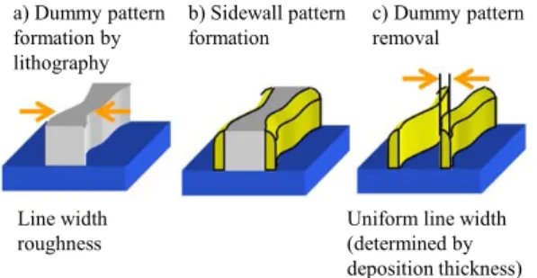
Fig. 2 Process steps of sidewall-transfer technique for the fabrication of narrow gate width FinFET.
2. Sample Fabriation
2.1 Process Flow
Planar MOSFET has a gate electrode on Si substrate, while gate electrodes surround Si substrate in fin FET to suppress the short channel e ff ect as the gate length is below 20 nm.
Figure 1 shows schematic view of our FinFET structure and process flow [3]–[10]. The Si surface of the channel was (110) because the FinFET was fabricated on standard (100) Si substrate. Narrow fins below 20 nm width were formed by side-wall transfer (SWT) technique [3], [4]. After RIE (Reactive Ion Etching) of Si, H
2annealing was carried out to improve the gate oxide quality and reduce trap density of the Si surface, the gate stack was formed by SiON gate dielectrics and poly-Si.
SWT technique and its process are shown in Fig. 2.
After SiO
2film deposition, the patterning was carried out
Copyright c ⃝ 2015 The Institute of Electronics, Information and Communication Engineers
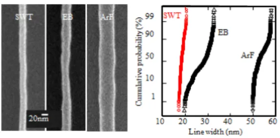
Fig. 3 Comparison of fin line width and variation in SWT, EB and ArF lithography and cumulative probability of line width after RIE are shown.
Each target of line width was set to the minimum size available in each lithography technology. SWT is successful in below 20 nm fin line with the small variation [10].
Fig. 4 Surface roughness with and without H2annealing. The roughness was improved by the annealing after dry etching.
by ArF lithography, which is used as dummy line. After SiN film was deposited on the patterned SiO
2film, sidewall spacer was fabricated by dry etching of SiN film and this region was used as hard mask for fin pattern during Si dry etching. The line to be formed by the sidewall spacer is nar- rower than the original dummy line pattern and has good LWR (Line Width Roughness) uniformity even if the uni- formity of the dummy SiO
2line width was poor because the line width is determined by the deposition thickness of SiN film not by lithography. The dummy SiO
2line is removed by wet treatment.
Figure 3 shows top-view SEM images and cumula- tive probability results of fine line patterns fabricated by SWT, EB lithography and ArF lithography, respectively.
The width is narrower and the uniformity in SWT technique is better than those in EB and ArF lithography as shown in cumulative probability results of line width. The better uni- formity of fin line width is e ff ective for suppression of larger drain current variation.
2.2 E ff ect of H
2Annealing
The performance of FinFET is very sensitive to the surface quality of the etched surface of the Si fin, which serves as the channel layer. It is therefore important to improve the surface quality of the Si fin. Figure 4 shows surface rough- ness of Si surface with and without H
2annealing after Si etching. The roughness was improved thanks to the anneal- ing because atomically flat or regularly arranged steps on the surface have been realized due to the migration of Si atoms on the surface during H
2annealing [9], [10]. In or- der to evaluate the quality of Si surface after H
2annealing,
Fig. 5 Interface trap density between Fin surface and gate oxide esti- mated by parallel-conductance method. The density becomes lower due to hydrogen anneal.
Fig. 6 The transconductance comparison for n- and p-FinFET with and without hydrogen anneal. These conductance are improved because of lower interface trap density.
the parallel conductance of MOS capacitor of FinFET was measured. The equivalent circuit of MOS structure of Fin- FET is shown in Fig. 5. R
g, C
oxand C
dare gate resistance, gate insulator capacitance and depletion capacitance under gate insulator, respectively. Y
itis the admittance of deple- tion region. The value of real part of Y
itdivided by mea- surement frequency (Y
it/ω ) is proportional to interface trap density between gate insulator and Si substrate. The divided Y
itof FinFET with H
2annealing is about 30% lower that without H
2annealing as shown in Fig. 5(a) and (b). These results show not only roughness of Si surface but also the quality of Si surface after Si etching is improved due to the H
2annealing process.
Figure 6 shows gate voltage dependence of transcon- ductance of both FinFET in linear region for n-FinFET and p-FinFET. The transconductance of FinFET with H
2anneal- ing process are larger than that without the annealing and the peak values of n-FinFET and p-FinFET become 24 and 28% larger, respectively. These should be attributed to the improvement of the mobility of electron and hole of FinFET due to improvement of Si surface quality.
3. Analog Performance
Lower flicker noise is essential requirement for analog /
Fig. 7 Fin width dependence of n-FinFET flicker noise and the variation of the noise. The noise and the variation become lower as the scaling of the width [12].
Fig. 8 Dependence potential profile on fin width. The slope of the po- tential in the channel becomes lower as shown in this figure. That means vertical electrical field from channel to gate electrode becomes relaxed.
This relaxation causes the decrease of trap rate and flicker noise [12].
mixed-signal circuits such as voltage controlled oscillator (VCO), analog-to-digital converter (ADC) and so on. It is therefore important to reduce the noise of FinFET for the application to those circuits. The noise characteristics of FinFET have been reported in some technical journals and conferences [12]–[15]. We focus on fin width dependence of the noise and analyze the dependence by using our sim- ulator for the first time. The H
2annealing was carried out to the measured samples because the noise is sensitive to the interface trap density between the gate insulator and Si substrate.
Figure 7 shows fin width dependence of n-FinFET input-referred flicker noise (S
vg) in saturation region. These noises are normalized by multiplying by gate area (L
gtimes W
g). The range of fin width was from 100 nm to 10 nm, and the gate length and total gate width were 1 µ m and 1 µ m, re- spectively. In this figure, average, minimum and maximum values in 40 devices are shown. It is clear that not only the noise itself but also the variation decreases as the fin width becomes below 50 nm. According to the results of substrate bias dependence of Vth, the FinFET with 100 nm fin width is in partial depletion mode, while those with below 50 nm fin width are in fully depletion mode like an ultra thin body FD silicon on insulator devices (UTB FD SOI devices).
To analyze the origin the noise reduction below 50 nm fin width, electric field from channel to gate electrode, which works as force to trap into gate insulator, is calculated by our device simulator as shown in Fig 8(a). The poten- tial of center of fin abruptly approaches the surface potential
Fig. 9 Parasitic resistance and capacitance for FinFET. Resistance of vertical gate electrode (Rg2), S/D (Rsd), capacitance of gate-Si sub.
(Cb01), gate-S/D (Cgds) and gate-S/D con. Region (Cgdsc) have large impact for RF performance [22].
with scaling fin width. As a result, the slope of the potential at Si surface decreases. This electric field works as the force to be trapped for electrons in the channel of FinFET. Figure 8(b) shows the fin width dependence of the electrical field at surface of channel calculated based on Fig. 8(a). The simu- lation results show the field is relaxed along with fin width narrowing. Some papers reported flicker noise of MOS- FET on UTB FD SOI devices with fully depletion mode and larger flicker noise reduction was observed [16]. We think the lower flicker noise with below 50 nm fin width is caused by the lower the electrical field. The minimum noise level of FinFET with below 50 nm fin width is satisfied with the requirement for 25 nm technology node in ITRS roadmap 2013 [17]. These results show FinFET is useful and appli- cable device for analog / mixed-signal circuits.
4. RF Performance
Some papers reported how to estimate parasitic resistance and capacitance [18]–[22] in scaled MOSFETs. We calcu- lated the transconductance and the gate capacitance based on these paper and estimated f
Tand f
maxof FinFET. Figure 9 shows schematic view of our multi finger FinFET struc- ture. To calculate f
Tand f
max, the parasitic capacitance and resistance are estimated with considering the following pa- rameters; gate length, fin width, gate width, finger length, fin pitch, fin height, STI depth, distance between gate elec- trode and source & drain contact region and the gate mate- rial. For example, when the impact of the gate resistance is calculated, not only top gate but also buried gate electrode between fins should be considered. The parasitic resistance of source and drain (R
sd) is calculated in considered of fin width and sheet resistance of Ni silicide. Gate capacitance to Si substrate between fins (C
b01) and coupling with source, drain contact region (C
gsdc) are also considered.
Figure 10 shows the simulation results of fin pitch dependence of f
Tand f
maxwhen gate length is 30 nm.
The main parameter is distance between gate electrode and
source, drain contact region (D). Both f
Tand f
maxincrease
as the fin pitch size decreases because of smaller C
b01. The
f
Tvalue, however, decreases significantly due to larger gate
capacitance (C
gsdc) when the source, drain contact region
closes to the gate electrode. When the material of buried
gate electrode is doped poly Si, f
maxdegrades at small fin
Fig. 10 Fin pitch dependence of fT and fmax. Parameter D is distance between gate and source, drain contact region [22].
Fig. 11 Dependence of fTon epitaxial Si thickness grown on Source and drain to reduce parasitic resistance [22].
Fig. 12 FTof nFinFET with the optimum layout design for RF perfor- mance. That is lower than planar nMOS below 20 nm gate length due to larger parasitic capacitance [22].
pitch due to increase of gate electrode resistance (R
g2). In our estimation, the most important device parameter is the finger length as well as planar MOSFET. Next, the distance between the gate and the source & drain contact region has higher impact to realize high f
Tand f
maxthan the fin pitch and the fin height.
When epitaxial Si growth on source and drain is ap- plied to reduce source and drain resistance, this unique S / D structure should be taken into consideration to evaluate the RF performance. Figure 11 shows the epitaxial Si thickness dependence of f
Twhen fin pitch is 50 nm. As epitaxial thick- ness increases, the f
Tincreases because the transconduc- tance increases by decrease of parasitic resistance of source and drain, however, further increase of the epitaxial Si thick- ness beyond 10 nm causes the decreases of f
Tbecause of the increase of parasitic capacitance between the gate and source, drain contact region (C
gsdc).
Figure 12 shows f
Tof nFinFET with the optimum lay-
show FinFET with longer gate length has the disadvantage for RF performance due to larger gate capacitance compar- ing with planar MOSFET [23].
Conclusion
Fin patterning due to Side-wall transfer (SWT) technique is useful to not only fabricate narrow fin line but also suppress fin width variation. The H
2annealing after Si etching is use- ful for not only to improve the mobility of electron and hole but also to reduce flicker noise of FinFET. The noise in Fin- FET with fully depletion mode decreases which are similar to UTSOI devices. However, FinFET has the disadvantage for RF performance due to larger gate capacitance compar- ing with planar MOSFET.
Acknowledgments
The authors would like to thank Atsushi Yagishita and Hi- rohisa Kawasaki for their useful research and development regarding to process and device technology for FinFET fab- rication.
References
[1] D. Lederer, B. Parvais, A. Mercha, N. Collaert, M. Jurczak, J.-P.
Raskin, and S. Decoutere, “Dependence of FinFET RF performance on fin width,” Proceeding of Silicon Monolithic Integrated Circuits in RF Systems 2006, pp.8–11.
[2] V. Subramanian, A. Mercha, B. Parvias, M. Dehan, G. Groeseneken, W. Sansen, and S. Decoutere, “Identifying the bottlenecks to the RF performance of FinFETs,” Proceedings of International Conference on VLSI Design 2010.
[3] Y. Choi, N. Lindert, P. Xuan, S. Tang, D. Ha, E. Anderson, T.-J.
King, J. Bokor, and C. Hu, “Sub-20 nm CMOS FinFET technolo- gies,” IEDM Tech. Dig., pp.421–424, Dec. 2001.
[4] A. Kaneko, A. Yagishita, K. Yahashi, T. Kubota, M. Omura, K.
Matsuo, I. Mizushima, K. Okano, H. Kawasaki, S. Inaba, T. Izumi- da, T. Kanemura, N. Aoki, K. Ishimaru, H. Ishiuchi, K. Suguro, K.
Eguchi, and Y. Tsunashima, “Sidewall transfer process and selective gate sidewall spacer formation technology for Sub-15nm FinFET with elevated source/drain extension,” IEDM Tech. Dig., pp.844–
847, Dec. 2005.
[5] L. Zhong, A. Hojo, Y. Matsushita, Y. Aiba, K. Hayashi, R. Takeda, H. Shirai, H. Saito, J. Matsushita, and J. Yoshikawa, “Evidence of spontaneous formation of steps on silicon (100),” Phys. Rev. B, vol.54, no.4, pp.R2304–R2307, July 1996.
[6] K. Okano, T. Izumida, H. Kawasaki, A. Kaneko, A. Yagishita, T.
Kanemura, M. Kondo, S. Ito, N. Aoki, K. Miyano, T. Ono, K. Ya- hashi, K. Iwade, T. Kubota, T. Matsushita, I. Mizushima, S. Inaba, K. Ishimaru, K. Suguro, K. Eguchi, Y. Tsunashima, and H. Ishiuchi,
“Process integration technology and device characteristics of CMOS FinFET on bulk silicon substrate with sub-10 nm Fin width and 20 nm gate length,” IEDM Tech. Dig., pp.487–490, Dec. 2005.
[7] K. Okano, T. Izumida, H. Kawasaki, A. Kaneko, A. Yagishita, T.
Kanemura, M. Kondo, S. Ito, N. Aoki, K. Miyano, T. Ono, K. Ya- hashi, K. Iwade, T. Kubota, T. Matsushita, I. Mizushima, S. Inaba, K. Ishimaru, K. Suguro, K. Eguchi, Y. Tsunashima, and H. Ishiuchi,
“Process integration technology and device characteristics of CMOS FinFET on bulk silicon substrate with sub-10 nm Fin Width and 20 nm gate length,” IEDM Tech. Dig., pp.50–53, Dec. 2006.
[8] S. Inaba, H. Kawasaki, K. Okano, T. Izumida, A. Yagishita, A.
Kaneko, K. Ishimaru, N. Aoki, and Y. Toyoshima, “Direct evalu- ation of DC characteristic variability in FinFET SRAM Cell for 32 nm node and beyond,” IEDM Tech. Dig., pp.487–490, Dec. 2007.
[9] H. Kawasaki, A. Kaneko, A. Yagishita, K. Okano, T. Izumida, T.
Kanemura, K. Suguro, K. Eguchi, Y. Tsunashima, S. Inaba, N. Aoki, K. Ishimaru, and Y. Toyoshima, “FinFET process and integration technology for high performance LSI in 22 nm node and beyond,”
Ext. Abs. the 7th International Workshop on Junction Technology 2007.
[10] S. Inaba, K. Okano, T. Izumino, A. Kaneko, H. Kawasaki, A. Yagi- shita, T. Kanemura, T. Ishida, N. Aoki, K. Ishimaru, K. Suguro, K.
Eguchi, Y. Tsunashima, Y. Toyoshima, and H. Ishiuchi, “FinFET:
The prospective multi-gate device for future So applications,” Pro- ceedings of ESSDERC 2006, pp.49–52.
[11] J.-S. Lee, Y.-K. Choi, D. Ha, S. Balasubramanian, T.-J. King, and J.
Bokor, “Hydrogen annealing effect on DC and low-frequency noise characteristics in CMOS FinFETs,” IEEE Trans. Electron Device Lett., vol.24, no.3, pp.186–188, Mar. 2003.
[12] T. Ohguro, K. Okano, T. Izumida, S. Inaba, N. Momo, K. Kokubun, H. S. Momose, and Y. Toyoshima, “Analysis of Fin width and tem- perature dependence of flicker noise for bulk-FinFET,” Proceedings of European Microwave Integrated Circuits Conference, pp.61–64, Sept. 2009.
[13] E. Simoen, M. Aoulaiche, N. Collaert, and C. Claeys, “Low- frequency noise in triple-gate n-channel bulk FinFETs,” Proceedings of International Conference on Noise and Fluctuations, 2011.
[14] M. Fan, V. Pi-Ho Hu, Y. Chen, Pi. Su, and C. Chuang, “Impacts of single trap induced random telegraph noise on FinFET devices and SRAM cell stability,” Dig. of Tech. Papers, VLSI Symp. on Tech- nol., June 2011.
[15] S. Wu, C. Lin, M. Chiang, J. Liaw, J. Cheng, S. Yang, M. Liang, T. Miyashita, C. Tsai, B. Hsu, H. Chen, T. Yamamoto, S. Chang, V. Chang, C. Chang, J. Chen, H. Chen, K. Ting, Y. Wu, K. Pan, R. Tsui, C. Yao, P. Chang, H. Lien, T. Lee, H. Lee, W. Chang, T.
Chang, R. Chen, M. Yeh, C. Chen, Y. Chiu, and Y. Chen, “A 16 nm FinFET CMOS technology for mobile SoC and computing applica- tions,” IEDM Tech. Dig., pp.224–227, Dec. 2013.
[16] M. Haartman, J. Hallstedt, J. Seger, B. Malm, P. Hellstrom, and M.
Osting, “Low-frequency noise in SiGe channel pMOSFETs n ultra- thin body SOI with Ni silicided source/drain,” Proc. Int. Conf. Noise and Fluctuation (INF), pp.307–310, 2005.
[17] http://www.itrs.net/
[18] M. Guillorn, J. Chang, A. Bryant, N. Fuller, O. Dokumaci, X. Wang, J. Newbury, K. Babich, J. Ott, B. Haran, R. Yu, C. Lavoie, D. Klaus, Y. Zhang, E. Sikorski, W. Graham, B. To, M. Lofaro, J. Tornello, D.
Koli, B. Yang, A. Pyzyna, D. Neumeyer, M. Khater, A. Yagishita, H. Kawasaki, and W. Haensch, “FinFET performance advantage at 22 nm: An AC perspective,” Dig. of Tech. Papers, VLSI Symp. on Technol., Kyoto, pp.12–13, June 2008.
[19] W. Wu, Z. Zhang, and M. Chan, “Parasitic minimization in RF multi-Fin FETs,” Proceedings of Electron Devices and Solid-State Circuits, 2005.
[20] A. Kranti, J. Raskin, and G. A. Armstrong, “Optimizing FinFET geometry and parasitics for RF applications,” Proceedings of Inter- national SOI Conference, 2008.
[21] S. Nuttinck, B. Parvais, G. Curatola, and A. Mercha, “Double-gate finFETs as a CMOS technology downscaling option: An RF Per- spective,” IEEE Trans. Electron. Devices, vol.54, no.2, pp.279–283, Feb. 2007.
[22] W. Wu and M. Chan, “Gate resistance modeling of multifin MOS devices,” IEEE Trans. Electron Device Lett., vol.27, no.1, pp.68–70, Jan. 2006.
[23] T. Ohguro, Y. Higashi, K. Okano, S. Inaba, and Y. Toyoshima,
“The optimum device parameters for high RF and analog/MS per- formance in planar MOSFET and FinFET,” Dig. of Tech. Papers, VLSI Symp. on Technol., Hawaii, pp.220–221, June 2012.
Tatsuya Ohguro He received the B.S. and M.S. degrees in physics from Hokkaido Uni- versity, Sapporo, Japan, in 1987, 1989, respec- tively. He joined Toshiba Corporation in 1989, where he has been engaged in the research and development of advanced CMOS devices and process for high performance logic, mixed sig- nal and RF circuits. He was a guest professor at Hiroshima University from 2003 to 2006. He is the recipient of Nikkei BP Grand Prize (1994), Yamazaki-Teiichi Prize (2007) and Commenda- tion for Science and Technology by the Minister of Education, Culture, Sports, Science and Technology (2009).
Satoshi Inaba He received the B.S. de- gree in applied physics, the M.S. degree in physics and the Ph.D. degree in applied physics all from Waseda University, Tokyo, Japan, in 1988, 1990 and 2006, respectively. He joined Toshiba Corporation, Kawasaki, Japan in 1990, where he was engaged in R&D for 0.1µm gate length CMOS and related device technology.
From 1998 to 2000, he was with IBM-Infineon- TOSHIBA 256 M bit DRAM Development Al- liance, Hopewell Junction, NY. From 2000, he was engaged in R&D of high performance and low power sub-50 nm CMOS devices including FinFETs. He was also with MIRAI-SELETE project, NSI Robust Transistor Design Program, Semiconductor Leading Edge Technologies (SELETE), Tsukuba, Japan from 2006 to 2011. He joined Toshiba Electronics Korea Corporation, Seoul, South Korea in 2012.
Since then, he has been engaged in memory device development for STT- RAM.
Dr. Inaba has served on the committees/sub-committees of several techni- cal conferences, including SSDM (2002–2004), IEDM (2003–2004), and Symp. on VLSI Technology (2008–2014). He is currently in charge of the technical program chair of 2015 Symp. on VLSI Tech.
Dr. Inaba is a member of the Physical Society of Japan, the Japan Soci- ety of Applied Physics and a senior member of the IEEE Electron Device Society. He is the recipient of SSDM Award (2014).
Akio Kaneko He received the B.S. and M.S. degrees in department of science and tech- nology from Keio University, Japan, in 1997, 1999, respectively. He joined Toshiba Corpora- tion in 1999, where he has been engaged in the research and development of advanced CMOS devices and process for high performance logic and memory.
ing Engineering Center, Semiconductor Com- pany, Toshiba Corporation, Kawasaki, Japan.
He is currently with the Center for Semiconduc- tor Research and Development, Semiconduc- tor Company, Toshiba Corporation, Yokkaichi, Japan, and has been engaged in the research and development of sub-50-nm CMOS devices and devices of peripheral circuit for NAND Flash memory.

![Fig. 10 Fin pitch dependence of f T and f max . Parameter D is distance between gate and source, drain contact region [22].](https://thumb-ap.123doks.com/thumbv2/123deta/5625444.1500151/4.892.98.403.113.279/pitch-dependence-parameter-distance-source-drain-contact-region.webp)
