Hideharu AMANO††,Senior Members, Masaaki KONDO††††,andMitaro NAMIKI†††††,Members
SUMMARY Power consumption has recently emerged as a first class design constraint in system LSI designs. Specially, leakage power has oc- cupied a large part of the total power consumption. Therefore, reduction of leakage power is indispensable for efficient design of high-performance system LSIs. Since 2006, we have carried out a research project called
“Innovative Power Control for Ultra Low-Power and High-Performance System LSIs”, supported by Japan Science and Technology Agency as a CREST research program. One of the major objectives of this project is re- ducing the leakage power consumption of system LSIs by innovative power control through tight cooperation and co-optimization of circuit technology, architecture, and system software designs. In this project, we focused on power gating as a circuit technique for reducing leakage power. Temporal granularity is one of the most important issue in power gating. Thus, we have developed a series of Geysers as proof-of-concept CPUs which pro- vide several mechanisms of fine-grained run-time power gating. In this pa- per, we describe their concept and design, and explain why co-optimization of different design layers are important. Then, three kinds of power gating implementations and their evaluation are presented from the view point of power saving and temporal granularity.
key words: low-power circuit techniques, fine grained power-gating, com- piler, system hierarchy cooperation
1. Introduction
Power consumption has recently emerged as a first class de- sign constraint in system LSI designs. Specially, leakage power has been a large factor in the total power consump- tion. Therefore, many research efforts have been paid for re- ducing leakage power so far to develop power-efficient sys- tem LSIs.
Many embedded processors and system LSIs provide a mechanism to reduce leakage power in a form of sleep mode which is realized by apower-knob in the hardware.
Typically, a large IP block such as a processor core goes into Manuscript received August 4, 2012.
†The author is with the Graduate School of Information Sci- ence and Technology, The University of Tokyo, Tokyo, 113-8656 Japan.
††The authors are with the Faculty of Science and Technology, Keio University, Yokohama-shi, 223-0061 Japan.
†††The authors are with the Department of Information Science and Engineering, Shibaura Institute of Technology, Tokyo, 135- 8548 Japan.
††††The author is with the Graduate School of Information Sys- tems, The University of Electro-Communications, Chofu-shi, 182- 8585 Japan.
†††††The author is with the Department of Computer and Informa- tion Sciences, Tokyo University of Agriculture and Technology, Koganei-shi, 184-8588 Japan.
a) E-mail: [email protected] DOI: 10.1587/transele.E96.C.404
a sleep mode when the system detects a Long idle period.
This kind of technique is effective if the entire IP block is in idle. However, as leakage power becomes a dominant factor of total power consumption,run-timeleakage power consumption has been a big concern and considered to be addressed.
Traditionally, run-time leakage power-saving tech- niques have been primarily used in cache memories. Those include cache decay [1] and drowsy cache [2] techniques.
Since some of cache lines are not necessarily utilized in a certain duration of program execution, the sleep mode is usually applied to each cache line individually. The gran- ularity of power-knob control in cache memory is spatially fine but temporally coarse.
A logic part in a CPU core could be a target of the run- time sleep mode control. The work in [3] tries to reduce the leakage power of functional units in a CPU core with power- gating technique. Since, the activity of each functional units depends on instructions cycle by cycle, the granularity of power-knob control should be temporally fine.
Dynamic sleep signal generation [4] tries to optimize sleep control dynamically without help of the software.
Loop-directed mothballing [5] attempts to increase the ac- curacy of predicting execution-unit requirements by ana- lyzing innermost loop bodies at runtime. On the contrary, compiler-based schemes [6]–[8], which employ static code analysis or dynamic profiling to identify the time period when a functional unit is not used, have also been proposed.
All of them rely on a technique of a single design layer:
architecture or compiler. Furthermore, they are based on simulation work, and there is no trial using a real chip.
Since 2006, we have carried out a research project called “Innovative Power Control for Ultra Low-Power and High-Performance System LSIs”, which is supported by Japan Science and Technology Agency as a CREST re- search program. One of the objectives of this project is re- ducing the leakage power consumption of system LSIs by innovative power control realized by tight co-operation and co-optimization of circuit technology, architecture, and sys- tem software. In this paper, we discuss several issues for fine-grained run-time power-gating and present the current outcome of the our research project. We also show the trade- offanalysis of fine-grained power gating methods for func- tional units in a CPU core.
Copyright c2013 The Institute of Electronics, Information and Communication Engineers
Fig. 1 Overview of power gating.
2. Geyser: A platform for Fine-Grained Power Gating
2.1 Fine-Grained Power-Gating
Power-gating with the MTCMOS technology is a well- known technique to reduce leakage power. In MTCMOS, power supply to logic blocks which consist of low-Vth tran- sistors is gated by high-Vth power-switch transistors. This puts power-gated units into sleep mode and no operation can be performed in these units. The power-switch transistors are inserted between a logic block and theVdd line or be- tween a logic block and theGroundline or both of them.
Figure 1 illustrates an overview of the power-gating cir- cuit when the power-switches are inserted between a logic block and the ground line. When the sleep signal is as- serted, the power switch transistors between ground (GND) line and virtual ground (VGND) line becomes off, and con- sequently power is gated and leakage current is suppressed.
We have applied three kinds of power gating implementa- tion whose detailed designs and evaluation are explained and discussed later in Sect. 3.
The mode transition between sleep and wake-up incurs the time and energy overheads due to the sleep signal propa- gation, power-switch driving, and discharging the electrical charge stored in parasitic capacitance on VGND-line. This is the reason why the granularity of power gating is coarse.
However, obviously finer temporal granularity is helpful to enlarge chances of power gating. Therefore, we have chal- lenged the ultimate fine granularity, that is, cycle-by-cycle power gating.
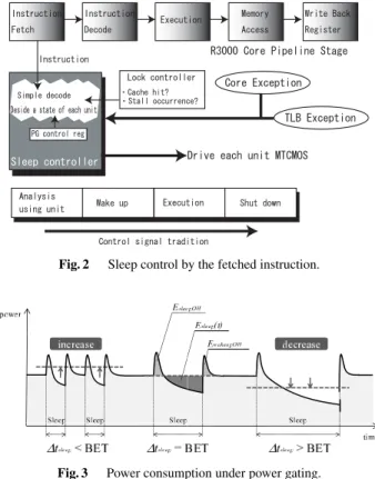
2.2 Dynamic Fine-Grained Power-Gating in Geyser We have been developingGeyseras a proof-of-concept CPU for run-time fine-grained power gating. The architecture of Geyser CPU core is MIPS R3000 [9], a 32 bit RISC pro- cessor widely used in embedded applications. Its instruc- tion pipeline consists of five stages, that is, Instruction Fetch (IF), Instruction Decode (ID), Execution (EX), Memory Ac- cess (MEM), and Write Back (WB).
As the target of fine-grained power-gating, we selected functional units in the EX stage, CLU (Common Arithmetic and Logic Unit), Shift unit, Multiplier unit, and Divider unit.
Their activity changes cycle by cycle but their average us- age ratio is not very high, and thus they are good targets for fine-grained power gating. It is easy to detect whether they
Fig. 2 Sleep control by the fetched instruction.
Fig. 3 Power consumption under power gating.
are used or not by observing fetched instructions. In Geyser, each functional unit has its own sleep signal which is gener- ated in the sleep controller as shown in Fig. 2. In this way, the spatial granularity of power gating is every functional unit in Geyser.
The other granularity is temporal. In Geyser, all the functional units except CLU are put into sleep mode auto- matically after the operation of the corresponding unit com- pletes. Whenever an instruction is fetched in the IF stage, the sleep controller detects the functional units used by the instruction. Each functional unit is used in EX stage. How- ever it takes a certain time to wake up a functional unit.
Thus, the detection is executed in the IF stage, which al- lows one cycle latency for the wake-up. As mentioned later, Geyser-2 successfully operates at 200 MHz, which indicates that all the functional units can wake up within 5 nsec. In this way, available temporal granularity of power gating is as fine as every cycle.
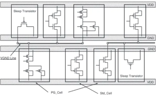
However, this naive cycle-by-cycle power gating does not necessarily lead to power reduction because power gat- ing itself consumes power. Therefore, sophisticated and novel power gating strategy is required.
2.3 Break-Even Time of Power Gating
Shutting offfunctional units as frequent as possible does not necessarily lead to power reduction because power gating itself consumes power. Power consumption under power gating is illustrated in Fig. 3. In this figure, EsleepOH and EwakeupOHrepresent energy overhead required to shut offand to wake up a functional unit respectively. Esleep(t) indicates
Esleep(BET)=EsleepOH+EwakeupOH (1)
2.4 Power Gating Control
Power must be shut off for a longer period than BET ex- plained in Sect. 2.3. However, the actual value of BET varies, as discussed in Sect. 4.2 later, between around ten cycles to a couple of hundreds of cycles. Thus, Geyser pro- vides the following two control mechanisms of power gat- ing.
• Power Gating under Cache Miss
• Power Gating directed by Compiler
The first one is cache-miss triggered power gating.
Geyser is an in-order processor and its instruction pipeline is stalled when instruction or data cache misses. Then, it is expected that all the functional units will not be used as long as cache miss penalty when cache miss occurs. Usu- ally cache miss penalty is quite long, this control is effective even for long BET.
The second one is effective for short BET. As men- tioned in Sect. 2.3, sleep period should be longer than BET.
Thus, it is necessary to find out how long each functional unit will not be used. We propose this compiler directed power gating based on the observation that compiler which schedules instructions can find out it. The detailed mecha- nisms is as follows.
Figure 4 shows an example of instructions with the PG direction support. In the MIPS R3000 ISA, when the high order 6 bits (op-code) are “000000”, the operation is ap- plied with the two registers shown in operand fields and the type of operation is indicated with the low order 6 bits. We use the high order 6 bits to indicate PG direction. After executing instructions whose high 6 bits are “000000”, the power supply to the target functional unit is cut off. Mean- while, after executing instructions whose high order 6 bits are “100111”, which is not define in the original ISA, the supply of power to the target functional unit is sustained.
The supply of power is sustained until executing the next instruction whose function is the same but the high order 6 bits are “000000”.
Fig. 4 Instructions with PG direction.
the supply of power to target functional after the execution.
Note that we do not have to wake up the functional units by instructions because they are known to be used when the instructions are fetched and will be waken up by the sleep controller shown in Fig. 2. Therefore, the roll of the com- piler is to determine when to turn the functional units offby compiler analysis.
The advantage of the proposed technique is that there is no need to add an additional hardware for prediction be- cause the prediction of the idle length is made statically dur- ing the compile time. Because the BET is predicted to be- come shorter in the future [11], applying power gating in a fine-grained time scale becomes more effective. However, in order to apply power gating effectively, we have to pre- cisely predict the idle time of the target units.
Power Gating Policy Register As mentioned above, Geyser provides two kinds of power gating strategy. In order to select the best one, we introduce a state register called PG policy register which stores the policies of PG as shown in Fig. 5. This register is managed by the operating system and control the PG strategy for each functional unit. Currently we have three policies as follows.
• Policy-1: The basic policy which shuts offevery unit dynamically after it is used by following the PG direc- tions of Fig. 4, and whenever any pipeline stall event occurs including a cache miss.
• Policy-2: Units are put in sleep mode only when a cache miss is detected.
• Policy-3: Units are never put into sleep mode.
2.5 Collaboration of Design Layers on Granularity of Power-Gating
In order to reduce power consumption effectively, the fol- lowing two features must be realized.
• BET must be shortened.
• Power must be shut offfor a period longer than the BET As BET is the minimum temporal granularity of power gating, shorter BET leads to more chances of power gating.
Fig. 5 PG policy register.
Fig. 6 Collaboration of design layers.
Therefore, how to shorten the BET is very important for en- ergy saving. BET heavily depends on the circuit design, especially the design of power gating. On the other hand, BET also depends on the environment, or more specifically, the temperature. For higher temperature, leakage power in- creases significantly and thusEsleepalso increases and BET gets short.
The actual value of BET is, as discussed in Sect. 4.2 later, varies between around ten cycles to hundreds of cy- cles. Under this wide variety of BET, we have to keep the condition that sleep period is longer than BET. Then, who is responsible to keep the condition? Our solution is as fol- lows.
First, for a given BET, architecture should be respon- sible for the best power gating control because architecture layer can observe and/or control the activity of a function unit tens of cycles from now on. More specifically, com- piler inserts PG directions by assuming a certain BET and PG strategy follows the Policy-1 described in Sect. 2.4. For long BET, as it is hard for compiler to identify long idle of functional units, Policy-2 is selected.
Second, OS or system software should be responsible for dynamic change of BET. More specifically, if the actual BET is shorter than that assumed by compiler, then PG strat- egy follows the Policy-1. If the actual BET is longer than compiler assumption but shorter than cache miss penalty, then PG strategy follows the Policy-2. Otherwise, Policy-3 is selected. OS changes the policy by updating the state reg- ister explained in Sect. 2.4. As the temporal granularity of temperature variation, in other word BET variation, is quite coarse, in the order of several milliseconds, OS can manage the change of PG strategy. The remaining issue is how to obtain the actual BET during execution. For this purpose, we have developed a leakage monitor [12].
This leakage monitor measures the actual leakage cur- rent. The relationship between the leakage current and BET is calibrated beforehand and referred by OS. In this way, we propose an effective run-time power-gating strategy based on tight co-operation and co-optimization of circuit technol- ogy, architecture, and system software as shown in Fig. 6.
Fig. 7 Cell based power gating.
3. Implementation Methods of Fine-Grained PG Fine-grained PG is a key technique of this project. Here, three fine-grained PG techniques are compared when they are used for run-time PG of functional units in Geyser CPU.
3.1 Cell-Based PG
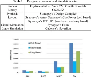
Cell-based FG-PG is the most flexible PG method originally proposed as a Locally-Shared Virtual ground scheme [13].
As shown in Fig. 7, a certain number of special standard cells (PG cells), in which the virtual ground (VGND) is sep- arated from the real ground are connected with the same VGND line, and they are shut-off with a sleep transistor.
Because existing ground rail in standard cell is used as the real ground, non-PG cells such as power switch drivers and isolation cells can be placed at any location. Since the size of power domain and the number of sleep transistors can be controlled freely, quick wake-up is possible if needed.
However, for this flexibility, a set of customized cells are needed for making a VGND pin inside each cell, and newly make a timing library for these cells. In general, it is difficult to modify all standard cells into PG cells because of the limitation of cost and design time. Moreover, additional area overhead caused by the VGND lines in modified cells becomes a problem during the implementation stage. The cell structure including VGND lines sometimes requires to stretch the cell height, and also increases the possibility of routing competition between signal wires.
Since modified cells and power switches are mixed with standard cells, the specialized design flow of layout is needed [14]. After the placement and routing of the lay- out, power switches are inserted by using Sequence De- sign’s CoolPower [15]†. Then, routing for power switches are done by using the routing function of the layout tool again.
3.2 Row-Based PG
Like cell-based PG, sleep transistors in the row-based PG
†Seqence Design was acquired by Apache Design Solution.
voltage drop problem as well as the cell-based PG. On the other hand, the power switched cells cannot be aligned with normal cells. Thus, the flexibility of cell placement is less than that in cell-based.
In row-based PG, specialized cells with virtual GND are not required. Thus, the routing competition between sig- nal wires does not occur. Also, the standard design method with Synopsys’s UPF (Unified Power Format) can be used for the layout.
3.3 Ring-Based PG
Ring-based PG is a commonly used for coarse-grained PG, but applicable to fine-grained PG if the electrical problems can be solved. The target PG domain is surrounded with a VGND ring shown in Fig. 9, and power switches are placed on the outside of VGND ring. Since entire power gated cells share a single VGND line, the instantaneous current from VGND to real ground is large enough to create inductively voltage fluctuations called ground bounce in the wake-up stage. Ground bounce not only has bad effort to neighbor- ing circuits which are executing normal operations, but also makes wake-up latency longer. To resolve this problem, we apply a structure in which power switches are turned in a
Fig. 8 Row based power gating.
Fig. 9 Ring based power gating.
4. Design and Evaluation
4.1 Design Environment and Simulation Setup
To simulate the PG effect, Fujitsu e-shuttle 65nm cell library is used for implementing the four functional units: ALU, shifter, multiplier and divider of Geyser-1 with each imple- mentation method, and unified power format (UPF) based design flow is used to create each power domain and in- sert or optimize the power switches for row-based and ring- based PG. The design tools and simulation setup are shown in Table 1. The operation frequency is set to be 200 MHz, and thus it means that wake-up latency must be within 5 ns.
Electric characteristics are evaluated by circuit level simula- tion, and the total leakage reduction when application pro- grams run is calculated with the results of the logic level simulation and the circuit level simulation.
4.2 Evaluation Results 4.2.1 Electric Characteristics
Figure 10 shows the area of each functional unit. It shows that row-based and ring-based PG can be implemented on about a half area of the cell-based PG due to the form of VGND routing. The difference between ring-based and row- based PG mainly comes from the overhead of buffer trees.
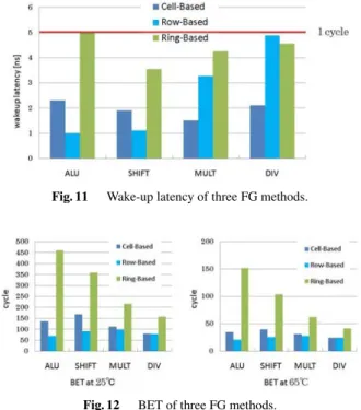
Wake-up latency is shown in Fig. 11. Due to the lim- itation of standard cell placer in row-based PG and ground
Table 1 Design environment and Simulation setup.
Process Fujitsu e-shuttle 65 nm CMOS with 12 metals
Library CS202SZ
Synthesis Sysnopsys’s Design Compiler
Layout Synopsys’s Astro, Sequence’s CoolPower (cell based) Synopsys’s ICC UPF (row based and ring based) Circuit Simulation Synopsys’s Hsim
Logic Simulation Cadence’s Ncverilog
Fig. 10 Area requirement of three FG power gating methods.
Fig. 11 Wake-up latency of three FG methods.
Fig. 12 BET of three FG methods.
bounce in ring-based PG, their wake-up latency is longer than that of cell-based, however both methods can achieve within 5ns by resizing power switches and adjusting buffer trees.
Since sleep-down and wake-up require a certain power consumption as well as the power for sleep control, fine- grained runtime PG has a risk to increase the power con- sumption if the sleep time is too short to compensate such overhead. Break Even Time (BET) which was introduced in previous sections is a useful measure for energy control.
As shown in Fig. 12, BET at 25C of each functional mod- ule is shorter with the row-based PG than with other two methods. That is, row-based PG has most chances that can sleep-down with the leakage reduction. On the other hand, ring-based PG, in which power consumption of buffer trees increases the total power overhead, has much longer BET.
4.2.2 Leakage Power Reduction
For evaluation of leakage power reduction during program execution, we run five programs for the embedded system:
QSORT, JPEG encoding, Dijkstra, Blowfish and CRC on Geyser. Figure 13 shows the result of leakage reduction with each benchmark. All three methods can reduce leak- age power by about 25% in JPEG encoding that multiplier and divider are used to some extent. On the other hand, in remaining benchmarks which use multiplier and divider less frequently, more than 50% of leakage power can be reduced.
Since leakage consumption in ring-based PG is much lower than other methods during long-sleep period, there is no big difference in leakage reduction even though BET is much worse than others.
Fig. 13 Leakage Reduction of three FG methods.
5. Real Chip Implementation
The evaluation results in the previous section suggest that row based method or ring based method is advantageous ex- cept the wake-up time. However, we used the cell based method in our first two prototype chips: Geyser-1 [14] and Geyser-2 [18] because of the following reasons. (1) Wake- up time is the most important issue for keeping correct op- eration of the CPU. (2) UPF based design was not available when the design of Geyser-1 started.
They were implemented on the same a 1.2 mm × 2.4 mm die. The utilized chip process, library and design tools are the same as shown in Table 1.
Figure 14 shows the chip photograph of Geyser-1. The main purpose of Geyser-1 is to examine the operation of the cell based PG and evaluate its effect with a real chip. Thus, it only provides the core CPU, and does not provide cache memory modules. As shown in Fig. 14, functional units are distributed on the chip. In Geyser-1, MULT module is larger than DIV module because of its high speed operation un- like DIV module which is designed with enough number of clock cycles. Since each instruction must be carried from outside the chip, the operational frequency is limited into 60 MHz.
The evaluation with the real chip reveals as follows: (1) The cell based PG used in Geyser-1 reduces the total power consumption of the processor core by 3%–8% at 25˚Cand 17%–29% at 80˚Cwhen benchmark programs run. (2) BETs of functional units are 640 (DIV) to 1080 (CLU) at 25˚C, and 80 (DIV) to 100 (CLU) at 100˚C.
The power reduction effect of the real chip were smaller than those of the circuit simulation. One reason is that the leakage power of the non-PG cells in real chips is much smaller than the circuit level evaluation by the im- provement of the process. The next reason is that the op- timization using CoolPower does not work well because of the lack of the experience.
Although Geyser-1 was the first real CPU chip with the run-time PG in the world, the operational frequency was not practical. Our second chip Geyser-2 provides the cache memory so that it can work at 200 MHz clock.
In order to reduce the wiring delay, Geyser-2 was im- plemented in the left half part of the chip (Fig. 15, but we must use the same chip size as Geyser-1 in order to keep
Fig. 14 Chip photo of Geyser-1.
Fig. 15 Chip photo of Geyser-2.
Fig. 16 Chip photo of Geyser-3.
enough number of I/O pins. Geyser-2 works with 210 MHz clock at maximum, and it is examined that all functional units can be activated from the sleep state with a clock cy- cle. That is, the wake-up time of the cell based PG is enough small. The leakage power reduction effect was improved compared with Geyser-1, but not so much. Detail evalua- tion results are shown in [19].
Since the evaluation results suggest that the row based or ring based PG is better than the cell based PG, and the design environment using UPF is available, we tried to im- plement Geyser-3 by using the ring based PG. Geyser-3 pro- vides TLBs and the co-processor for Linux operating system and a wireless interconnect mechanism for inter-chip com- munication.
As shown in Fig. 16, Geyser-3 CPU is also imple- mented in the left half part of the chip, and the right half part is used for test circuits of wireless interconnect. Although both Linux and Kaimon, the embedded operating system, are working on Geyser-3, the ring based power gating does not work because of a design problem on triple well struc- ture.
Fig. 17 Photo of Geyser and mother board.
Linux and Kaimon have a process scheduler based on BET with performance counter monitoring the power gat- ing states in Geyser. The process scheduler controls the PG policy register to reduce power consumption. The current chip is mounted on an FPGA mother board including main memory, secondary memory such as compact flash, serial line and other I/Os. OSs and application programs are run- ning on the board (Fig. 17) to evaluate the architecture. We have solved the problem, and the re-made version of Geyser- 3 will be available in September, 2012. We will evaluate the real chip, and demonstrate the effect of integrated power control with collaboration of design layer.
6. Conclusions
A co-optimization of circuit technology, architectures and system software designs on fine-grained runtime power gat- ing for functional units in an embedded CPU is introduced.
Three power gating methods: cell based, row based and ring based are evaluated and compared when they are used in a run-time power gating of functional units in an embedded CPU. Simulation results suggested that from the viewpoint of wake-up time, the cell based method is advantageous, while area and reduction of the leakage power of row based and ring based are better than those of the cell based.
Geyser-1 and Geyser-2 implemented with the cell based PG demonstrated the effect of fine-grained runtime power gating with running benchmark programs. Geyser-3 with the ring based PG will be available soon, and we will and demonstrate the effect of integrated power control with collaboration of design layer with a real chip.
Acknowledgments
This research was performed by the author for STARC as part of the Japanese Ministry of Economy, Trade and Indus-
try sponsored “Next-Generation Circuit Architecture Tech- nical Development” program. The authors thank to VLSI Design and Education Center (VDEC) and Japan Science and Technology Agency (JST) CREST for their support.
References
[1] S. Kaxiras, Z. Hu, and M. Martonosi, “Cache decay: Exploiting generational behavior to reduce cache leakage power,” Proc. 28th ISCA, pp.240–251, June 2001.
[2] K. Flautner, N. Kim, S. Martin, D. Blaauw, and T. Mudge, “Drowsy caches: Simple techniques for reducing leakage power,” Proc. 29th ISCA, p.148.
[3] Z. Hu, A. Buyuktosunoglu, V. Srinvasan, V. Zyuban, H. Jacobson, and P. Bose, “Microarchitectural techniques for power gating of ex- ecution units,” Proc. ISLPED, pp.32–37, Aug. 2004.
[4] A. Youssef, M. Anis, and M. Elmasry, “A comparative study be- tween static and dynamic sleep signal generation techniques for leakage tolerant designs,” IEEE Trans. Very Large Scale Integr.
(VLSI) Syst., vol.16, no.9, pp.1114–1126, Sept. 2008.
[5] C.A. Court and P.H.J. Kelly, “Loop-directed mothballing: Power gating execution units using runtime loop analysis,” IEEE Micro, vol.31, no.6, pp.29–38, 2011.
[6] W. Zhang, M. Kandemir, N. Vijaykrishnan, M. Irwin, and V. De,
“Compiler support for reducing leakage energy consumption,” De- sign, Automation and Test in Europe Conference and Exhibition, 2003, pp.1146–1147, IEEE, 2005.
[7] S. Rele, S. Pande, S. Onder, and R. Gupta, “Optimizing static power dissipation by functional units in superscalar processors,” in Com- piler Construction, pp.85–100, Springer, 2002.
[8] S. Roy, N. Ranganathan, and S. Katkoori, “A framework for power- gating functional units in embedded microprocessors,” IEEE Trans.
Very Large Scale Integr. (VLSI) Syst., vol.17, no.11, pp.1640–1649, 2009.
[9] E. Farquhar and P. Bunce, The MIPS Programmer’s Handbook, Morgan Kaufmann Publishers, 1994.
[10] T. Komoda, H. Sasaki, M. Kondo, and H. Nakamura, “Compiler- directed fine grain power gating for leakage power reduction in mi- croprocessor functional units,” Proc. ODES2009, 2009.
[11] J.A. Butts and G.S. Sohi, “A static poewr model for architects,” Proc.
33rd Micro, pp.191–201, 2000.
[12] K. Usami, Y. Goto, K. Matsunaga, S. Koyama, D. Ikebuchi, H.
Amano, and H. Nakamura, “On-chip detection methodology for break-even time of power gated function units,” Proc. ISLPED2011, pp.241–246, 2011.
[13] K. Usami and N. Ohkubo, “An approach for fine-grained run-time power gating using locally extracted sleep signals,” IEEE 24th Inter- national Conference on Computer Design, 2006. ICCD2006, 2008.
[14] D. Ikebuchi, N. Seki, Y. Kojima, M. Kamata, Z. Lei, H. Amano, T. Shirai, S. Koyama, T. Hashida, Y. Umahashi, H. Masuda, H.
Usami, S. Takeda, H. Nakamura, M. Namiki, and M. Kondo,
“Geyser-1: A MIPS R3000 CPU core with fine grain runtime power gating,” IEEE Solid-State Circuits Conference, 2009, A- SSCC 2009, IEEE Asian, pp.281–284, 2009.
[15] I. Sequence Design, “Cool power,” www.sequencedesign.com [16] S. Kim, S. Kosonocky, and D. Knebel, “Understanding and mini-
mizing ground bounce during mode transition of power gating struc- tures,” Proc. 2003 ISLPED, pp.22–25, 2003.
[17] I.C. Society, “IEEE standard for design and verification of low power integrated circuits,” IEEESTD.2009.4809845, March 2009.
[18] Z. Lei, D. Ikebuchi, Y. Saito, M. Kamata, N. Seki, Y. Kojima, H. Amano, S. Koyama, T. Hashida, Y. Umahashi, D. Masuda, K.
Usami, T. Sunata, K. Kimura, A.S.M. Namiki, H. Nakamura, and M. Kondo, “Geyser-1 and Geyser-2: MIPS R3000 CPU chips with fine-grain runtime power gating,” IEEE 13th Symposium on Low- Power and High-Speed Chips, 2010, CoolChips 2010, pp.161–163,
2010.
[19] Z. Lei, D. Ikebuchi, K. Usami, M. Namiki, M. Kondo, H. Nakamura, and H. Amano, “Design and implementation fine-grained power gat- ing on microprocessor functional units,” IPSJ Trans. System LSI De- sign Methodology, pp.182–192, 2011.
Hiroshi Nakamura is a professor in the De- partment of Information Physics and Comput- ing at the University of Tokyo. His research in- terests include low-power VLSI design, power- aware computing, high-performance computer systems and dependable computing. He has a PhD in electrical engineering from the Univer- sity of Tokyo. He is a member of IEEE, the ACM, and IPSJ.
Waihan Wang is a master course student, Graduate School of Science and Technology, Keio University. His research interests include low power CPU design.
Yuya Ohta received an MS in Information Science and Engineering at the Shibaura Insti- tute of Technology in March, 2012. Now, he works for Hitach Ltd.
Kimiyoshi Usami is a professor in the De- partment of Information Science and Engineer- ing at the Shibaura Institute of Technology. His research interests include energy-aware comput- ing and ultra-low voltage design. He has a PhD in electric engineering from Waseda University.
He is a member of IEEE and the ACM.
Masaaki Kondo is an associate professor in the Graduate School of Information Systems at the University of Electro-Communications in Tokyo. His research interests include computer architectures, high-performance computing, and dependable computing. He has a PhD in electri- cal engineering from the University of Tokyo.
He is a member of IEEE, the ACM and IPSJ.
Mitaro Namiki is a professor in the Faculty of Engineering at the Tokyo University of Agri- culture and Technology. His research interests include operating systems, programming lan- guages, parallel processing, and computer net- works. He has a PhD in computer science from the Tokyo University of Agriculture and Tech- nology. He is a member of the ACM and IPSJ.