鳥取大学研究成果リポジトリ
Tottori University research result repository
タイトル
Title
Advanced Performance of Annealed Ni-P/(Etched Si)Negative Electrodes for Lithium-Ion Batteries著者
Auther(s)
Domi, Yasuhiro; Usui, Hiroyuki; Narita, Masakuni;Fujita, Yoshihiro; Yamaguchi, Kazuki; Sakaguchi, Hiroki掲載誌・巻号・ページ
Citation
Journal of the Electrochemical Society , 164 (13) :A3208 - A3213刊行日
Issue Date
2017-10-24資源タイプ
Resource Type
学術雑誌論文 / Journal Article版区分
Resource Version
著者版 / Author権利
Rights
© 2017 The Electrochemical Society.DOI
10.1149/2.1211713jesAdvanced Performance of Annealed Ni–P/(Etched Si) Negative Electrodes for Lithium–Ion Batteries
Yasuhiro Domi,a,b,* Hiroyuki Usui,a,b Masakuni Narita,a,b Yoshihiro Fujita,a,b Kazuki Yamaguchi,a,b and Hiroki Sakaguchia,b,z,*
a Department of Chemistry and Biotechnology, Graduate School of Engineering, Tottori University,
Minami 4–101, Koyama–cho, Tottori 680–8552, Japan
b Center for Research on Green Sustainable Chemistry, Tottori University, Minami 4–101, Koyama–
cho, Tottori 680–8552, Japan
[email protected]–u.ac.jp, [email protected]–u.ac.jp, [email protected], [email protected], [email protected], [email protected]–u.ac.jp
* Electrochemical Society Active Member. z Corresponding authors:
E–mail address: [email protected]–u.ac.jp (Hiroki Sakaguchi) Tel/Fax: +81–857–31–5265
Abstract
The electrochemical performance of variously treated Ni–P–coated Si (Ni–P/Si) negative electrodes for lithium-ion batteries was investigated. X–ray diffraction analysis revealed the formation of nickel silicide (NiSi and NiSi2) after annealing, which improved the adhesion between the Ni–P coating layer and Si particles. Spotty Ni–P particles did not aggregate on an etched Si surface due to an anchor effect, even after annealing, whereas the particles aggregated on an untreated Si surface. An annealed Ni–P/(etched Si) negative electrode maintained a discharge capacity of 2000 mA h g–1 even at the 100th cycle in an organic electrolyte, which can be attributed to Ni–P particles remaining on the surface of the annealed Ni–P/(etched Si) electrode even after the charge–discharge test. The annealed Ni–P/(etched Si) electrode also exhibited superior cycle performance with a reversible capacity of 1000 mA h g–1 over 750 and 1100 cycles in an organic electrolyte containing film–forming additive and an ionic liquid electrolyte, respectively. Consequently, the annealed Ni– P/(etched Si) electrode achieved both high reversible capacity and long cycle life.
1. Introduction
To diffuse the use of electric vehicles (EVs), it is necessary to increase mileage per charge. Lithium–ion batteries (LIBs) with high energy density and long cycle life would help to raise the range of EVs. Silicon (Si) is a potential candidate as an active material for the negative electrode of next–generation LIBs due to its high theoretical capacity of 3580 mA h g–1 (Li3.75Si) and a negative working potential close to that of lithium metal. The crystalline Si phase forms a crystalline Li3.75Si phase at such negative potential via an amorphous LixSi alloy phase.1–6 However, the volumetric
change ratio per Si atom from Si to Li3.75Si corresponds to 380%, which generates high stresses and large strains in the active materials. The accumulation of strains during repeated charge–discharge cycles causes disintegration of the active material layer, which results in poor cycle performance of the Si electrode. In addition, Si has a low diffusion coefficient for Li+ and a low electrical conductivity.7,8 These limitations have hindered the practical application of a Si negative electrode in LIBs.
To address these issues, various approaches have been proposed, including doping of Si with impurities to reduce the electrical resistivity and/or to change its properties including its morphology, crystallinity, and phase transition,9–12 application of a film–forming additive or an ionic liquid electrolyte to form a stable surface film,13–16 and coating Si with carbon to increase its low electrical conductivity.17,18 When a compound consisting of Si and another elements, called a silicide, is used instead of elemental Si as the active material for a negative electrode, the discharge capacity dramatically decreases due to the smaller amount of Li stored in the silicide.19,20 Therefore,
to take advantage of the huge theoretical capacity of Si, we believe that elemental Si should be a main component of the active material of the negative electrode for next–generation LIBs. Composite electrodes composed of elemental Si and other materials that compensate for the disadvantages of the Si are useful.We previously investigated the electrochemical performance of various composite electrodes that consisted of elemental Si and a silicide such as LaSi2/Si19,20 or Fe–Si/Si,21 or of elemental Si and a metal (metal–coated Si).22–25 These composite materials have been shown to require four main properties; (1) mechanical properties to release the stress due to Si, (2) high electronic conductivity, (3) moderate reactivity with Li+, and (4) high thermodynamic stability so that they will not decompose under repeated charge–discharge cycles.20,21
Various metal (Ni,22 Ru,23 and Cu24 layers, and Ni/Cu25 multilayers)–coated Si composite thick–film electrodes were prepared by the electroless deposition (ELD)26,27 and a successive gas– deposition (GD)28 methods. A Ni–P–coated Si (Ni–P/Si) electrode notably exhibited good cycle performance; the Ni–P/Si electrode showed an initial reversible capacity of 2610 mA h g–1 at the 20th cycle and maintained a discharge capacity of 780 mA h g–1 even after 1000 cycles in 1 M LiClO4 dissolved in propylene carbonate (PC).22,29 The Ni–P coating layers on the Si particles can play important roles in increasing the electrical conductivity of the active material and in releasing the stress induced by a change in the volume of Si. In addition, we demonstrated that the Ni–P layer consists of Ni and Ni3P based on the selected area electron diffraction (SAED) pattern, and the Ni3P would act as a diffusion pathway for Li because it reacts moderately with Li+ according to the following equation:30
Ni3P + 3Li+ + 3e- → 3Ni + Li3P (1)
While the cycle performance of a Ni–P/Si electrode was superior to that of a Si–alone electrode, the high discharge capacity of the Ni–P/Si electrode still faded within the initial 100 cycles, which results from exfoliation of the Ni–P coating layers from Si particles.
Other researchers have also investigated the electrochemical performance of various metal–coated Si electrodes.31–34 Kim et al. found that a Au–coated Si nanowire/graphene composite electrode shows 1520 mA h g–1 after 20 cycles in LiPF6–based electrolyte solution.31 Baek et al. reported that a Ag–coated Si nanowire electrode maintains a reversible capacity of ca. 710 mA h g–1 after 30 cycles in LiPF6–based electrolyte solution with 10 wt% fluoroethylene carbonate.32 The cyclability of these coated Si electrodes was superior to that of an untreated Si–alone electrode, which can be attributed to an increase in the electrical conductivity of Si due to the coating layer of Au or Ag. However, the cycle performance for long cycle has not yet been investigated.
In the present study, variously treated Ni–P/Si powders were synthesized to achieve no capacity fading over long cycle and the electrochemical performance of them as a negative electrode for LIBs was investigated. Chemical etching of Si particles and subsequent annealing of Ni–P/(etched Si) were carried out to roughen the surface of Si particles and to improve the adhesion of the coating layer to Si particles, respectively. It is expected that these treatments suppress the exfoliation of Ni–P coating layers from Si particles. In addition, the effect of a film–forming additive and an ionic liquid electrolyte on the electrochemical performance of the annealed Ni– P/(etched Si) electrode was also investigated.
2. Experimental
Synthesis and Characterization. ––– We designed various treatments for Ni–P/Si powders, and commissioned Hitachi Metals Neomaterial, Ltd. to prepare them. Removal of a natural dioxide film on the Si surface accompanied by roughening of the surface was performed by chemical etching with hydrofluoric acid. Etched or untreated Si was coated with Ni–P particles by the ELD method,22,29 and the powders were subsequently annealed at various temperature in an inert gas atmosphere.
To confirm the crystal structures of the obtained powders, X–ray diffraction (XRD, Ultima IV, Rigaku) measurement was performed at a voltage of 40 kV and a current of 40 mA with Cu–Kα radiation. A backscattered electron (BSE) image and an energy–dispersive X–ray spectroscopy (EDS) of the Ni–P/Si powders were obtained by field–emission scanning electron microscopy (FE– SEM, JSM–6701F, JEOL Co., Ltd.). The beam acceleration voltage and working distance were set at 20 kV and 8 mm (15 mm for EDS) for BSE measurement, respectively. The surface of Ni–P/Si particles was coated with gold to prevent a charge–up. The surface morphology and root–mean– square roughness (Sq) of Ni–P/Si electrodes were investigated by confocal laser scanning microscopy (CLSM, VK–9700, Keyence).
Electrode Preparation and Electrochemical Measurement. ––– The working electrode was prepared by the gas–deposition (GD) method, and the detailed conditions of GD were reported
previously.11,13 Li sheets (Rare Metallic, 99.9%, thickness; 1mm) served as the reference and/or counter electrodes. The electrolyte solution used was 1 mol dm–3 (M) lithium bis(trifluoromethanesulfonyl)amide (LiTFSA) dissolved in PC (Kishida Chemical Co., Ltd.), PC containing 5 vol% vinylene carbonate (VC), and N–methyl–N–propylpyrrodinium bis(fluorosulfonyl)amide (Py13–FSA). A laboratory–made beaker–type three–electrode cell and 2032–type coin cell were used for electrochemical measurements. A glass–fiber separator was used in the coin cell. The above two types of cells were assembled in an Ar–filled glovebox (Miwa MFG, DBO–2.5LNKP–TS) with an oxygen concentration below 1 ppm and a dew point below –100oC.
A galvanostatic charge–discharge test was carried out using an electrochemical measurement system (HJ1001SM8, Hokuto Denko Co., Ltd. or BS2506, KEISOKUKI) in a potential range between 0.005 and 2.000 V vs. Li+/Li at 303 K. The current density was set at 0.36 A g–1 (0.1 C) in the 1st cycle and 1.44 A g–1 (0.4 C) after the 2nd cycle, unless otherwise noted. The weight of active materials was that of variously treated Ni–P/Si, except for Si–alone electrode.
3. Results and Discussion
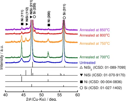
Characterization of Variously Treated Ni–P/Si Powders. ––– Figure 1 shows XRD patterns of Ni– P/Si powders annealed at various temperatures. The result of untreated Ni–P/Si powder is also shown for comparison. Peaks assigned to Si (220), Si (311), Ni (111), and Ni (200) were confirmed for all samples. While the peak intensity of Ni (111) and Ni (200) increased when the powder was annealed at 700oC, it decreased over 750oC. In addition, a peak arising from NiSi (112) appeared
after annealing at 750oC, and its peak intensity decreased over 800oC. These changes in the peak intensity reflect that the crystallinity of Ni increased up to 700oC, and that some of the Ni atoms in the coating layer diffused into the Si particles and a NiSi phase formed at 750oC. While it has been reported that a NiSi2 phase forms after annealing at 800oC,35,36 definitive XRD peaks of NiSi2 were not confirmed because these peaks overlap those of Si. However, the NiSi phase should transform to a NiSi2 phase over 800oC taking into account of disappearance of the peak arising from NiSi phase. Nickel silicides (NiSi and NiSi2) ought to form at the interface between the Ni–P coating layer and Si particles. We previously reported that the Ni–P coating layer contained Ni3P based on the SAED pattern.29 However, the XRD pattern did not show peaks that could be assigned to Ni3P, which indicates that the Ni3P content in this layer is very low.
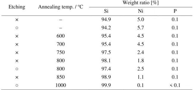
The weight ratio of Si, Ni, and P in the powders used in this study is summarized in Table 1, which was confirmed by Inductively Coupled Plasma Atomic Emission Spectroscopy (ICP–AES). While the Ni–P layer was coated on the Si surface in the same way as before annealing, the weight ratio of Si and Ni increased and decreased over 750oC, respectively. The Ni–P coating layer was dissolved in aqua regia and was analyzed by ICP–AES. However, NiSi and NiSi2 are insoluble in aqua regia, as with Si. Therefore, it is considered that these nickel silicides were not detected by ICP–AES and the weight ratio of elemental Ni decreased over 750oC, as shown in Table 1. Hereafter, we will focus on an annealing temperature of 800oC unless otherwise described because an electrode consisting of Ni–P/Si powder annealed at 800oC exhibited a superior cycle performance (discussed later). Figure S1 shows XRD patterns of variously treated Ni–P/Si powders.
Peak shifts and new peaks were not confirmed by etching and/or annealing. The peak intensity of Ni (111) in Ni–P/(etched Si) and annealed Si–P/(etched Si) powders was greater than that in untreated and annealed Ni–P/Si powders. Because the surface area of Si particles increased by etching, the coating amount of Ni would increase.
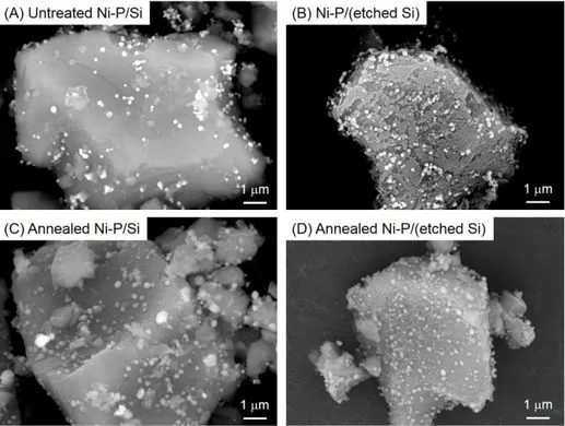
BSE images of variously treated Ni–P/Si powders are shown in Figure 2. BSE images reflect the electron density of the sample, i.e., light and dark spots in Figure 2 correspond to Ni–P and Si, respectively. EDS maps and the spectra also revealed that the bright particles were Ni–P, as shown in Figures S2 and S3. Spotty Ni–P particles that ranged in size from tens of nanometers to ca. 200 nm were deposited on the smooth surface of untreated Si particles, as shown in Figure 2A. Similar Ni–P particles were also deposited on the roughened surface of etched Si particles (Figure 2B). Ni–P particles grew to a maximum diameter of 500 nm after annealing, as shown in Figure 2C, which indicates that adjacent Ni–P particles cohered to each other. On the other hand, Ni–P particles did not aggregate on an etched Si surface, as shown in Figure 2D. Ni–P particles would not diffuse on the etched Si surface due to an anchor effect, even after annealing.
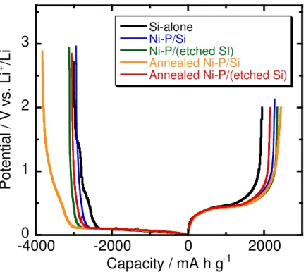
Advanced Performance of Variously Treated Ni–P/Si Negative Electrodes. ––– Figure 3 shows the first charge–discharge curves of variously treated Ni–P/Si and Si–alone electrodes in 1 M LiTFSA/PC. For the Si–alone electrode, potential plateaus were observed in charge and discharge curves at around 0.1 and 0.4 V vs. Li+/Li, respectively. These plateaus are attributed to the alloying and de–alloying reactions of Si with Li.1,5 On the other hand, all of the treated electrodes also
showed similar potential plateaus at the same potentials. While Ni in the Ni–P coating layer is inactive against Li, the reversible lithiation and delithiation reactions of Ni–P/Si electrodes proceeded, since Ni–P particles were distributed in a patchy fashion on the Si surface and Ni3P in Ni–P particles shows moderate reactivity with Li+.30These results indicate that various treatments, such as etching and annealing, do not affect an interfacial resistance.
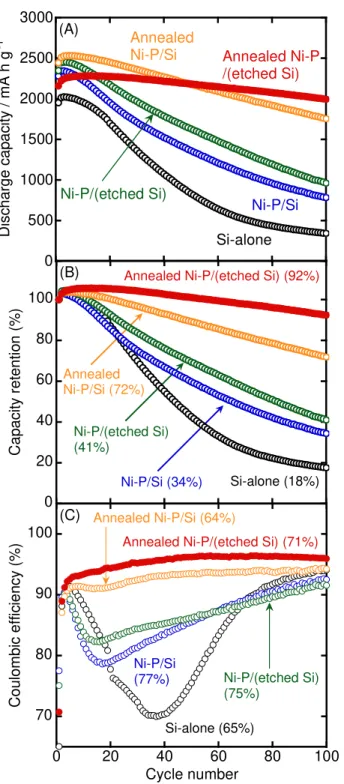
Figure 4A shows the cycle performance of variously treated Ni–P/Si electrodes. For comparison, the result of a Si–alone electrode is also shown. Figure 4B shows the dependence of capacity retention on the cycle number. The percentage in parentheses indicates the capacity retention at the 100th cycle. The discharge capacity of the Si–alone electrode rapidly decayed, which can be attributed to deterioration of the Si electrode due to the significant change in the volume of Si during charge–discharge reactions. On the other hand, the capacity fading of an untreated Ni–P/Si electrode was suppressed. We previously reported that the mechanical properties of Si particles were improved by Ni–P coating; i.e., the elastic modulus of Si increased with Ni–P coating.22,29 This means that the spotty Ni–P coating layer can effectively release the stresses from Si. In addition, the electrical resistivity of untreated Ni–P/Si powders (200 Ω cm) was only one-eightieth that of Si powders (16000 Ω cm), and Ni3P, which shows moderate reactivity with Li+, was contained in the coating layer. It is considered that these improved properties suppress the disintegration of the Si electrode and the loss of electric contact with the current collector. However, the high discharge capacity of the Ni–P/Si electrode still faded within the initial 100 cycles. On the other hand, the annealed Ni–P/Si electrode exhibited better performance; a discharge capacity of ca.
1750 mA h g–1 and a capacity retention of 72% were confirmed at the 100th cycle. It is considered that nickel silicides (NiSi and NiSi2) improve the adhesion between the Ni–P coating layer and the Si particles. The coating layer should not exfoliate from the Si particles during the charge–discharge cycle and the deterioration of the Si electrode should be suppressed; thus the performance of the annealed Ni–P/Si electrode was improved compared to that of an untreated Ni–P/Si electrode. The cyclability of a Ni–P/(etched Si) electrode was almost the same as that of an untreated electrode. On the other hand, the annealed Ni–P/(etched Si) electrode showed significantly improved cycle performance; the discharge capacity and capacity retention were 2000 mA h g–1 and 92% at the 100th cycle, respectively. These results demonstrated that adhesion of the Ni–P coating layer to Si particles was not improved by etching alone, while adhesion was improved by annealing of Ni– P/(etched Si) because the Ni–P particles should not diffuse on the etched Si surface due to an anchor effect even after the annealing.
Figure 4C shows the dependence of the Coulombic efficiency of the variously treated electrodes on the cycle number. The percentage in parentheses indicates the efficiency at the first cycle. At about the 40th cycle, a drop in the Coulombic efficiency of the Si–alone electrode was observed. This drop was suppressed in the order annealed Ni–P/(etched Si) > annealed Ni–P/Si > Ni–P/(etched Si) > untreated Ni–P/Si > Si–alone electrodes. It is well known that a surface film is formed through reductive decomposition of the electrolyte solution, which causes a decrease in the Coulombic efficiency. The resulting film should collapse with the significant change in the volume of Si during lithiation–delithiation processes, and then a surface film should form again on the
newly exposed Si surface. Hence, the deterioration of the electrode would be gradually suppressed according to the above order. In addition, the adhesion between the Ni–P coating layer and Si particles should increase improved by various treatments, such as etching and annealing, because the cycle performance of the Ni–P/Si electrodes improved according to the above order. Figure S4 shows the cycle performance of electrodes consisting of Ni–P/Si powders annealed at various temperatures. The performance was improved with an increase in the annealing temperature, and the Ni–P/Si electrode annealed at 800oC achieved a superior performance. However, the electrode annealed at a higher temperature (1000oC) exhibited inferior cyclability; there should be an optimum anneal temperature.
To clarify a mechanism of improved cycle performance of annealed Ni–P/Si and annealed Ni–P/(etched Si) electrodes, we observed a surface morphology of these electrodes. CLSM images of untreated and annealed Ni–P/Si electrodes after the 100th cycle are shown in Figure 5. For comparison, CLSM images before cycling are shown in Figure S5. The Sq value of the untreated and annealed Ni–P/Si electrodes was 0.48 and 0.46 µm before cycling, respectively; the roughness was almost the same regardless of annealing. After the 100th cycle, on the other hand, the values for the untreated and annealed Ni–P/Si electrodes were 6.05 and 4.00 µm, respectively; since the Sq value of the latter was lower than that of the former, disintegration of the annealed electrode was suppressed. It is considered that an increase in adhesion between the Ni–P coating layer and Si due to annealing maintains the functions of Ni–P layers, such as moderate reactivity with Li+, high electrical conductivity, and superior mechanical properties for releasing the stresses induced by the
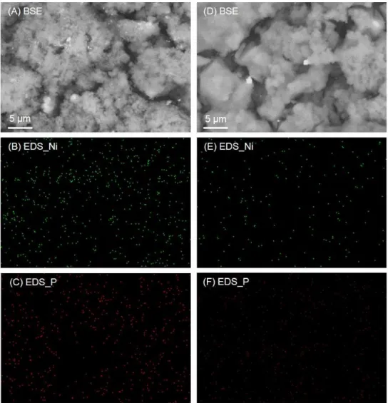
change in volume of Si. In addition, Ni–Si (nickel silicide) phases formed by annealing should react with Li+ and act as a diffusion pathway for Li.37Figure 6 shows BSE images and the corresponding EDS maps of the annealed Ni–P/(etched Si) and untreated Ni–P/Si electrodes after the 40th cycle. As for the annealed Ni–P/(etched Si) electrode, bright spots were observed in BSE image and elemental Ni and P were detected in EDS maps (Figure 6A–6C). In case of untreated Ni–P/Si electrode, on the other hand, there were fewer bright spots and almost no Ni or P was detected, as shown in Figure 6D–6F. These results demonstrated that the Ni–P coating layer remains on the annealed Ni–P/(etched Si) surface after charge–discharge cycles due to improved adhesion of the coating layer to Si particles.
Figure 7 shows the rate performance of various Ni–P/Si electrodes in 1 M LiTFSA/PC. As is the case in Figure 4, the initial discharge capacity of these electrodes was almost the same at 0.4 C. Even at a rate of 10 C, the discharge capacities of annealed Ni–P/(etched Si) and annealed Ni– P/Si electrodes were 460 and 470 mA h g–1, respectively. These capacities are about 3.6 times greater than that of an untreated Ni–P/Si electrode. The capacity retention values for annealed Ni– P/(etched Si) and annealed Ni–P/Si electrodes were 98 and 97 % at the 60th cycle after the rate had returned to the initial rate (0.4 C), respectively, whereas the retention of untreated Ni–P/Si electrode was 62 %. The superior rate performance and capacity retention are believed to result from an increase in the utilization ratio of Si; the above–mentioned effects of Ni–P coating on Si become marked because the coating layer remained on the annealed electrodes even after charge–discharge cycling. On the other hand, the effects of Ni–P coating disappeared due to exfoliation of the coating
layer from untreated Ni–P/Si electrode surface.
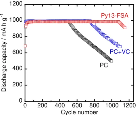
Cycle Performance in Functional Electrolyte Solutions. ––– We previously reported that a Si– alone negative electrode exhibited a superior electrochemical performance in some functional electrolytes, such as organic electrolytes containing film–forming additives and ionic liquid electrolytes, compared to conventional organic electrolyte solutions.13,16 Surface films formed in these functional electrolytes should be more stable and act as protective film to prevent continuous decomposition of the electrolytes, leading to suppress the disintegration of the Si electrode. It has also been reported that a capacity limitation dramatically improved the cycle performance of a Si– alone electrode,38 since the accumulation of severe stress was suppressed by moderation of the change in the volume of Si. Therefore, we investigated the cycle performance of the annealed Ni– P/(etched Si) electrode under a charge capacity limitation of 1000 mA h g–1 in PC–based electrolyte containing VC as a film–forming additive and in Py13–FSA–based electrolyte as an ionic liquid electrolyte, as shown in Figure 8. In 1 M LiTFSA/PC, the annealed Ni–P/(etched Si) electrode maintained the discharge capacity of 1000 mA h g–1 until the 500th cycle. On the other hand, a Si– alone electrode could not maintain the discharge capacity of 1000 mA h g–1 beyond the 100th cycle in the same electrolyte solution (data not shown).
In the VC–containing electrolyte and Py13–FSA–based electrolyte solutions, the annealed Ni–P/(etched Si) electrode maintained a discharge capacity of 1000 mA h g–1 over 750 and 1100 cycles, respectively; the electrode exhibited a significantly improved cycle performance. Compared
to PC–based electrolyte, the cycle life of the electrode was increased 2.2–fold in the Py13–FSA– based electrolyte. There have been almost no reports about a Si–based electrode with both high reversible capacity and long cycle life. Consequently, it is noteworthy that the annealed Ni– P/(etched Si) electrode achieved excellent cycle performance with a discharge capacity of 1000 mA h g–1 beyond the 1000th cycle in Py13–FSA–based electrolyte.
4. Conclusion
The electrochemical performance of variously treated Ni–P/Si negative electrodes for LIBs was investigated. Variously treated Ni–P/Si powders were characterized by XRD, ICP–AES, SEM, and EDS; an annealing resulted in the formation of nickel silicides (NiSi and NiSi2), which improve the adhesion between the Ni–P coating layer and the Si particles. While Ni–P particles cohered to each other on the smooth surface of Si after annealing at 800oC, they did not aggregate on an etched Si surface due to an anchor effect, even after annealing. The electrochemical performance of Ni– P/Si electrode was significantly improved by etching of Si and subsequent annealing of Ni– P/(etched Si); the electrode maintained a discharge capacity of 2000 mA h g–1 and a capacity retention of 92% even at the 100th cycle. This superior cyclability was attributed to the improved adhesion of the Ni–P coating layer to the Si particle surface due to the etching of Si and subsequent annealing of Ni–P/(etched Si). An annealing temperature of 800oC would be optimum in a temperature range from 600 to 1000oC. In addition, the rate performance of the annealed Ni– P/(etched Si) and annealed Ni–P/Si electrodes was superior to that of the untreated electrode. In a
performance with a discharge capacity of 1000 mA h g–1 over 1100 cycles.
Acknowledgement
This work was partially supported by the Japan Society for the Promotion of Science (JSPS) KAKENHI, Grant Numbers JP17K17888, JP17H03128, JP16K05954. The authors gratefully acknowledge Mr. Ryoji Inoue (Hitachi Metals Neomaterial Ltd.) and Mr. Ken Asada (Hitachi Metals Neomaterial Ltd.) for their assistance with the synthesis of variously treated Ni–P powders.
References
1. T. D. Hatchard and J. R. Dahn, J. Electrochem. Soc., 151, A838 (2004).
2. M. N. Obrovac and L. Christensen, Electrochem. Solid–State Lett., 7, A93 (2004).
3. K.Ogata, E. Salager, C. J. Kerr, A. E. Fraser, C. Ducati, A. J. Morris, S. Hofmann, and C. P. Grey,
Nat. Commun., 5, 3217 (2014).
4. X. H. Liu, L. Zhong, S. Huang, S. X. Mao, T. Zhu, and J. Y. Huang, ACS Nano, 6, 1522 (2012). 5. M. N. Obvovaca and L. J. Krause, J. Electrochem. Soc., 154, A103 (2007).
6. Y. Kubota, M. C. S. Escaño, H. Nakanishi, and H. Kasai, J. Appl. Phys., 102, 053704 (2007). 7. N. Ding, J. Xu, Y. X. Yao, G. Wegner, X. Fang, C. H. Chen, and I. Lieberwirth, Solid State
Ionics, 180, 222 (2009).
8. J. Xie, N. Imanishi, T. Zhang, A. Hirano, T. Takeda, and O. Yamamoto, Mater. Chem. Phys., 120, 421 (2010).
9. B. R. Long, M. K. Y. Chan, J. P. Greeley, and A. A. Gewirth, J. Phys. Chem. C, 115, 18916 (2011).
10. Z. Wen, and F. Tian, Int. J. Electrochem. Sci., 8, 10129 (2013).
11. Y. Domi, H. Usui, M. Shimizu, Y. Kakimoto, and H. Sakaguchi, ACS Appl. Mater. Interfaces, 8, 7125 (2016).
12. F. Legrain and S. Manzhos, J. Power Sources, 274, 65 (2015).
13. Y. Domi, H. Usui, M. Shimizu, K. Miwa, and H. Sakaguchi, Int. J. Electrochem. Sci., 10, 9678 (2015).
14. T. Sugimoto, Y. Atsumi, M. Kono, M. Kikuta, E. Ishiko, M. Yamagata, and M. Ishikawa, J.
Power Sources, 195, 6153 (2010).
15. C. C. Nguyen and S.–W. Song, Electrochem. Commun., 12, 1593 (2010).
16. K. Yamaguchi, Y. Domi, H. Usui, M. Shimizu, K. Matsumoto, T. Nokami, T. Itoh, and H. Sakaguchi, J. Power Sources, 338, 103 (2017).
17. X. Zhou, Y.–X. Yin, A.–M. Cao, L.–J. Wan, and Y.–G. Guo, ACS Appl. Mater. Interfaces, 4, 2824 (2012).
18. S. Y. Kim, J. Lee, B.–H. Kim, Y.–J. Kim, K. S. Yang, and M.–S. Park, ACS Appl. Mater.
Interfaces, 8, 12109 (2016).
19. H. Sakaguchi, T. Iida, M. Itoh, N. Shibamura, and T. Hirono, IOP Conf. Ser.: Mater. Sci. Eng., 1, 012030 (2009).
20. Y. Domi, H. Usui, Y. Takemoto, K. Yamaguchi, and H. Sakaguchi, J. Phys. Chem. C, 120, 16333 (2016).
21. H. Usui, K. Nouno, Y. Takemoto, K. Nakada, A. Ishii, and H. Sakaguchi, J. Power Sources, 268, 848 (2014).
22. H. Usui, M. Shibata K. Nakai, and H. Sakaguchi, J. Power Sources, 196, 2143 (2011). 23. H. Usui, Y. Kashiwa T. Iida, and H. Sakaguchi, J. Power Sources, 195, 3649 (2010). 24. H. Usui, H. Nishinami T. Iida, and H. Sakaguchi, Electrochemistry, 78, 329 (2010). 25. H. Usui, N. Uchida, and H. Sakaguchi, J. Power Sources, 196, 10244 (2011).
26. T. Cetinkaya, M. Uysal, M. O. Guler, H. Akbulut, and A. Alp, Powder Technol., 253, 63 (2014).
27. G. Talla, R. K. Guduru, B. Q. Li, and P. S. Mohanty, Solid State Ionics, 269, 8 (2015).
28. H. Sakaguchi, T. Toda, Y. Nagao, and T. Esaka, Electrochem. Solid–State Lett., 10, J146 (2007).
29. H. Usui, N. Uchida, and H. Sakaguchi, Electrochemistry, 80, 737 (2012).
30. J. Y. Xiang, J. P. Tu, X. L. Wang, X. H. Huang, Y. F. Yuan, X. H. Xia, and Z. Y. Zeng, J.
Power Sources, 185, 519 (2008).
31. H.–J. Kim, S. E. Lee, J. Lee, J.–Y. Jung, E.–S. Lee, J.–H. Choi, J.–H. Jung, M. Oh, S. Hyun, and D.–G. Choi, Physica E, 61, 204 (2014).
32. S.–H. Baek, J.–S. Park, Y.–M. Jeong, and J.–H. Kim, J. Alloys Compd., 660, 387 (2016).
33. H. Park, S. Lee, S. Yoo, M. Shin, J. Kim, M. Chun, N.–S. Choi, and S. Park, ACS Appl. Mater.
Interfaces, 6, 16360 (2014).
34. J. W. Kim, J. H. Ryu, K. T. Lee, and S. M. Oh, J. Power Sources, 147, 227 (2005).
35. C. M. Liu, W. L. Liu, S. H. Hsieh, T. K. Tsai, and W. J. Chen, Appl. Surf. Sci., 243, 259 (2005). 36. H. F. Hsu, H. Y. Chan, T. H. Chen, H. Y. Wu, S. L. Cheng, and F. B. Wu, Appl. Surf. Sci., 257, 7422 (2011).
37. W.–R. Liu, N.–L. Wu, D.–T. Shieh, H.–C. Wu, M. H. Yang, C. Korepp, J. O. Besenhard, and M. Winter, J. Electrochem. Soc., 154, A97 (2007).
Figure Captions
Figure 1 X–ray diffraction patterns of Ni–P/Si powders annealed at various temperatures.
Figure 2 Backscattered electron images of (A) untreated Ni–P/Si, (B) Ni–P/(etched Si), (C) annealed Ni–P/Si, and (D) annealed Ni–P/(etched Si) powders.
Figure 3 Charge–discharge curves of various Ni–P/Si electrodes during the 1st cycle in 1 M LiTFSA/PC.
Figure 4 Dependence of (A) discharge capacity, (B) capacity retention, and (C) Coulombic efficiency of variously treated Ni–P/Si electrodes. The electrolyte used was 1 M LiTFSA/PC. The percentage at parentheses in parts (B) and (C) indicates the capacity retention at the 100th cycle and the efficiency at the first cycle, respectively.
Figure 5 Confocal laser scanning microscopy images of (A) untreated and (B) annealed Ni–P/Si electrodes after the 100th charge–discharge cycle in 1 M LiTFSA/PC.
Figure 6 (A and D) Backscattered electron images and (B, C, E and F) energy–dispersive X–ray spectroscopy maps. (A–C) Annealed Ni–P/(etched Si) and (D–F) untreated Ni–P/Si electrodes were cycled for 40 cycles in 1 M LiTFSA/PC.
Figure 7 Rate performance of various Ni–P/Si electrodes in 1 M LiTFSA/PC. Blue, orange, and red symbols show the untreated Ni–P/Si, annealed Ni–P/Si, and annealed Ni–P/(etched Si) electrodes, respectively.
Figure 8 Cycle performance of annealed Ni–P/(etched Si) electrodes in 1 M LiTFSA dissolved in PC, PC containing 5 vol.% VC, and Py13–FSA under a constant charge capacity of 1000 mA h g-1.
40 45 50 55 60 In te n s it y / a .u . 2θ (Cu-Kα) / deg. ○ Si (ICSD: 01-027-1402) ■ Ni (ICSD: 00-004-0836) ▼ NiSi (ICSD: 01-070-9170) △ NiSi 2 (ICSD: 01-089-7095) Untreated Annealed at 700oC Annealed at 750oC Annealed at 800oC Annealed at 850oC ■ N i (1 1 1 ) ▼ N iS i (1 1 2 ) ○ S i (2 2 0 ) ■ N i (2 0 0 ) ○ S i (3 1 1 ) ▼ N iS i (2 1 1 )
Figure 2 Backscattered electron images of (A) untreated Ni–P/Si, (B) Ni–P/(etched Si), (C) annealed Ni–P/Si, and (D) annealed Ni–P/(etched Si) powders.
0
1
2
3
-4000
-2000
0
2000
Si-alone Ni-P/Si Ni-P/(etched SI) Annealed Ni-P/SiAnnealed Ni-P/(etched Si)
P
o
te
n
ti
a
l
/
V
v
s
.
L
i
+/L
i
Capacity / mA h g
-1Figure 3 Charge–discharge curves of various Ni–P/Si electrodes during the 1st cycle in 1 M LiTFSA/PC.
Figure 4 Dependence of (A) discharge capacity, (B) capacity retention, and (C) Coulombic efficiency of variously treated Ni–P/Si electrodes. The electrolyte used was 1 M LiTFSA/PC. The percentage at parentheses in parts (B) and (C) indicates the capacity retention at the 100th cycle and the efficiency at the first cycle, respectively.
0 500 1000 1500 2000 2500 3000 Annealed Ni-P /(etched Si) Annealed Ni-P/Si D is c h a rg e c a p a c it y / m A h g -1 Ni-P/Si Ni-P/(etched Si) Si-alone (A) 0 20 40 60 80 100
Annealed Ni-P/(etched Si) (92%)
Annealed Ni-P/Si (72%) Ni-P/Si (34%) Si-alone (18%) Ni-P/(etched Si) (41%) (B) C a p a c it y r e te n ti o n ( % ) 70 80 90 100 0 20 40 60 80 100 Cycle number C o u lo m b ic e ff ic ie n c y ( %
) Annealed Ni-P/(etched Si) (71%)
Annealed Ni-P/Si (64%) Ni-P/Si (77%) Ni-P/(etched Si) (75%) Si-alone (65%) (C)
Figure 5 Confocal laser scanning microscopy images of (A) untreated and (B) annealed Ni–P/Si electrodes after the 100th charge–discharge cycle in 1 M LiTFSA/PC.
Figure 6 (A and D) Backscattered electron images and (B, C, E and F) energy–dispersive X–ray spectroscopy maps. (A–C) Annealed Ni–P/(etched Si) and (D–F) untreated Ni–P/Si electrodes were cycled for 40 cycles in 1 M LiTFSA/PC.
0
500
1000
1500
2000
2500
3000
0
10
20
30
40
50
60
Cycle number
0.4 C
1 C
2 C
5 C
10 C
0.4 C
D
is
c
h
a
rg
e
c
a
p
a
c
it
y
/
m
A
h
g
-1Figure 7 Rate performance of various Ni–P/Si electrodes in 1 M LiTFSA/PC. Blue, orange, and red symbols show the untreated Ni–P/Si, annealed Ni–P/Si, and annealed Ni–P/(etched Si) electrodes, respectively.
0
200
400
600
800
1000
1200
0
200
400
600
800 1000 1200
D
is
c
h
a
rg
e
c
a
p
a
c
it
y
/
m
A
h
g
-1Cycle number
Py13-FSA
PC
PC+VC
Figure 8 Cycle performance of annealed Ni–P/(etched Si) electrodes in 1 M LiTFSA dissolved in PC, PC containing 5 vol.% VC, and Py13–FSA under a constant charge capacity of 1000 mA h g-1.
Table 1 Various Ni-P/Si powders used in this study.
Etching Annealing temp. / oC Weight ratio [%]
Si Ni P × – 94.9 5.0 0.1 ○ – 94.2 5.7 0.1 × 600 95.4 4.5 0.1 × 700 95.4 4.5 0.1 × 750 97.5 2.4 0.1 × 800 98.1 1.8 0.1 ○ 800 97.4 2.5 0.1 × 850 98.9 1.1 0.1 ○ 1000 99.9 0.1 < 0.1