平山量子光素子研究室
Quantum Optodevice Laboratory 主任研究員 平山 秀樹(工博) HIRAYAMA, Hideki (Dr. Eng.)
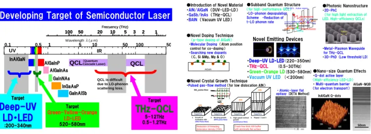
【日本語版】 キーセンテンス: 1. ワイドギャップ窒化物半導体の結晶成長技術の開拓 2. 深紫外LED、半導体レーザの開発 3. テラヘルツ量子カスケードレーザの開発 キーワード: 量子光デバイス、量子電子デバイス、レーザダイオード、発光ダイオード、深紫外発光素子、テラヘルツ 量子素子、半導体結晶成長、窒化物半導体、半導体超格子 研究目的 深紫外(波長200-350nm)やテラヘルツ(THz)周波数帯の半導体レーザ、LED など、これまで実現が難 しかった未開拓周波数領域の半導体発光素子は、殺菌や医療、高密度光記録、半導体照明、生化学産業、 化学工業、各種非破壊・透視検査など広範囲にわたる新たな応用分野への展開が期待され、それらの開発 が強く求められている。当研究室では、新規半導体材料の結晶成長技術の開拓、ならびに、原子・ナノス ケールで制御された人工構造による電子・光制御技術の導入などにより、未踏波長領域発光素子などの革 新的な機能を有する半導体発光素子を実現する研究を行っている。これまで、ワイドギャップ半導体の新 規結晶成長法の考案による世界最高品質結晶の実現とそれを用いた発光効率の飛躍的向上や、新しい原理 に基づく量子へテロ構造・フォトニックナノ構造の導入などにより、実現が難しいとされてきた未踏領域 の深紫外LED、THz 半導体レーザを実現し、さらにそれらの限界性能の追及を行ってきた。未踏波長素子 の実現とそれらの高性能化により様々な応用分野が切り開かれ、今後の産業の発展への大きな貢献が期待 される。 1、ワイドバンドギャップ窒化物半導体の結晶成長技術の開拓と深紫外 LED の開発(平山、定、前田、Khan、 Yun、南) 波長が 220-350nm の深紫外 LED・半導体レーザは、医療、殺菌・浄水、高密度光記録、照明、生化学 産業、化学工業、公害物質の高速分解など、幅広い分野での応用が考えられ、その実現が大変に期待され ている。しかし、深紫外発光素子を実現する上で最も有望なAlGaN 系混晶半導体は、結晶の欠陥が多く発 図 1. 半導体レーザの実現波長領域と開発目 標としている未開拓領域 図 2. 未開拓波長発光デバイス実現のた めに投入している新規半導体技術 未開拓波長半導体光デバイスの新展開 開発目標 深紫外 高効率LD・LED :200-340nm 真空紫外: <200nm 開発目標 THz-QCL 5-12THz帯 0.5-1.2THz帯 室温発振 開発目標 緑-黄-橙 高効率LD・LED 520-580nm ・深紫外LD・LED(220-350nm) ・THz-QCL (0.5-30THz) ・緑-黄-橙LD (530-580nm) ・真空紫外LED (<200nm) ●新規半導体材料の導入 ・AlN/AlGaN系(DUV-LED・LD) ・GaSb/InAs系(THz-QCL) ・InAsSb/InP系(THz-QCL) ・BAlN系(真空紫外LED) ●新規結晶成長技術 ・パルス供給多段成長法 ・ELO(横方向埋め込み)成長法 (AlN系の貫通転位の低減、 光取り出し効率向上) ・DETA法(Droplet Eliminated by Thermal Annealing) (GaN系QCLの原子層平坦成長) ●新規ドーピング技術 (AlGaNの高濃度p型化) ・分子ドーピング技術 (原子位置制御コドーピング法) ・新しいドーパントの探索 (C、SiとMg、MgとOなど) ●新規サブバンド量子構造 (THz-QCLの高性能化) ・3準位系量子構造の 対角遷位の制御 ・4準位系量子構造 ・間接注入型量子構造 ●新規光制御構造 ・2Dフォトニック結晶 (QCLの高機能化・LEDの 光取り出し効率向上) ・DMWプラズモン導波路 (QCLの低閾値・高温動作) ・3Dフォトニック結晶 (無閾値・超高効率LD) ・高反射p型電極 ●ナノサイズ量子効果 ・量子ドット発光層 (LED・LDの高効率化) ・多重量子障壁(MQB) (電子輸送の制御) 未開拓波長光デバイス doping THz-QCL Active region: LO phononDepopulation THz-Emission Injection Injection
AlNのELO成長 AlGaN/GaN-QCL成長 InAlGaN量子ドット
AlGaN-MQB 50nm AlGaN Mg Mg MgMg Si Si SiSi Mg Mg Si Si Mg Mg Si Si
光効率が著しく低減するなどLED 素子の開発は難しかった。 本研究では、高品質AlGaN 系混晶半導体の結晶成長技術の開拓を新規に行い、世界最短波長の高効率深紫 外 LED を実現した。「アンモニアパルス供給多段成長法」という新しい結晶成長法を考案し、世界最高品 質AlN 結晶の実現、それを用いて内部量子効率の飛躍的改善(100 倍程度)を達成した。また、In 組成変 調領域への電子・ホールの局在効果 を用いて80%程度の非常に高い内部 量子効率も実現した。さらに、多重 量子障壁(MQB)を用いた電子リーク 制御法による注入効率の向上、光取 り出し効率の改善などを行うことで、 最短波長領域 220-280nm の高効率 LED を世界に先駆けて実現した。得 られた深紫外LED は殺菌、医療応用 などにおいて実用レベルの高出力を すでに達成している。本年度の成果 としては、世界最高効率である外部 量子効率20.3%を記録し、水銀ラン プの効率に迫る値を実現する事で、 各応用分野への普及の可能性を大い に広めた。今後、技術をさらに発展 させ、青色 LED と同等の高効率化の 実現、紫外レーザダイオード(LD)の 実現、真空紫外LED などへの展開が期待される。
2、GaAs 及び GaN 系半導体を用いたテラヘルツ量子カスケードレーザの開発(平山、寺島、林、Wang Ke、 Wang Li、福田) 光と電波の間の周波数領域に位置するテラヘルツ光は、電波の透過性と、光の取り扱いやすさや高分解 能など両方の性質を兼ね備えているため、各種非破壊・透視検査など幅広い応用分野において期待されて いる。テラヘルツ量子カスケードレーザ(THz-QCL)は、小型・高効率、長寿命、連続出力、安価なテラ ヘルツ光源としてその実現が期待されている。しかし THz-QCL は現在開発途上にあり、動作周波数は 1-5THz に限られており、また低温動作しか得られていない。本研究では精度の高い結晶成長技術を駆使し GaAs 系及び GaN 系 QCL 構造を実現し、その高温動作において世界をリードしている。間接注入型量子 構造を採用することにより、低周波数QCL における世界最高動作温度(1.89 THz, 160K)を実現し、さら に、LO フォノンエネルギー増加法を用いた室温動作実現にも取り組んでいる。また、現在実現が不可能と されている5-12THz の QCL の実現を目指し、新たに GaN 系半導体を用いた QCL の実現の試み始めてい る。今年度は、GaAs 系 THz-QCL で 250mW の高出力動作に成功した。また、GaN 系 THz-QCL で誘導 放出光の観測に成功した。 p-Al0.77Ga0.23N;Mg 多重AlNバッファー層 (NH3パルス供給成長法) n-Al0.77Ga0.23N;Si バッファー層 Ni/Au p電極 p-GaN;Mg コンタクト層 サファイア基板 Ni/Au n電極 UV 放射出力 Al0.62Ga0.38N(1.5nm)/ Al0.77Ga0.23N(6nm) 3層 量子井戸発光層 Al0.95Ga0.05N;Mg(4nm)/ Al0.77Ga0.23N;Mg(2nm) 5層 多重量子障壁電子 ブロック層 Al0.77Ga0.23N;Mg 200 250 300 350 400 450 波長 (nm) L ED 発光強度(ピーク値で規格化) AlGaN-QW DUV LEDs 室温測定 222~261nm InAlGaN-QW DUV LED 282~351nm 最高外部量子効率5%@280nm(室温CW動作)
AlGaN系深紫外LEDの開発(波長222-351nm)
図3. 実現したAlGaN 系半導体深紫外LED(波長 222-351nm) の構造と動作スペクトル 0 200 400 600 800 1000 1200 1400 1600 1800 In te n s ity [a .u .]Current density [A/cm2
] 4K 20K 40K 60K 80K 100K 120K 143K 2.5 3.0 3.5 4.0 4.5 5.0 In te n si ty [a .u .] Frequency [THz] Lasing at 3.7 THz GaAs/Al0.15Ga0.85As THz QCLs Max Op.Temp. :143K 200 μm
THz-QCLの開発 (3.7THz、最高動作温度150K)
図4. GaAs 系テラヘルツ量子カスケードレーザの素子概観と発振動作特性 ---
【English】
Key Sentence :
1. Development of crystal growth technique for wide-bandgap nitride semiconductors 2. Development of deep-UV LEDs and laser diodes
3. development of terahertz quantum cascade lasers
Key Word : Quantum optodevice, Quantum electronic device, Laser diode, Light-emitting diode, Deep-ultraviolet emitting device, Terahertz quantum device, Semiconductor crystal growth, Nitride semiconductor, Semiconductor superlattice
Purpose of Research
The development of new-frequency semiconductor light sources, such as deep-ultraviolet (DUV) light-emitting diodes (LEDs) and laser diodes (LDs), or terahertz quantum-cascade lasers (THz-QCLs) is one of the most important subjects, because they are required for a wide variety of potential applications, i. e., sterilization, water and air purification, medicine and biochemistry, light sources for high density optical recording, white light illumination or non-destructive seeing-through examinations. Quantum Optodevice Laboratory is studying to stand at the forefront of optics and nanotechnology, e.g. in creating innovative optical device including undeveloped frequency semiconductor emitters, and develop a new research field through merging advanced optical/laser science, atomic/nano-scale material fabrication technology, and novel semiconductor crystal growth technologies and so forth. Through the introduction of the novel crystal growth technology for wide-gap semiconductors, we have achieved innovative emitting devices such as highly-efficient DUV-LEDs with shortest wavelength regime (220-350nm), or THz-QCLs. We have also investigated the performance-limit of these devices by introducing innovative quantum heterostructures and/or photonic nano-structures. Through the creation of the applicable field of these new emitting devices, we aim for contributing to the realization of rich human being society.
1. Development of AlGaN-based semiconductor crystal growth techniques and realization of deep-UV Fig. 1. Development target for new-frequency
semiconductor light-emitting devices Fig. 2. Innovative semiconductor techniques introduced for achieving undeveloped-frequency light-emitting devices 0.1 0.5 1 5 10 50 100 50 Wavelength λ(μm) UV IR QCL QCL GaInAlSb InGaAsP GaInNAs AlGaInAs AlGaInP InAlGaN (Quantum Cascade Laser) 100 50 20 10 5 3 2 1 Frecuency (THz) 100 50 20 10 5 3 2 1 Frecuency (THz)
Developing Target of Semiconductor Laser
QCL is difficult due to LO-phonon scattering loss. Target
Deep-UV
LD・LED
:200-340nm TargetTHz-QCL
5-12THz 0.5-1.2THz Target Green-Yellow-Orange LD・LED 520-580nm ・Deep-UV LD・LED(220-350nm) ・THz-QCL (0.5-30THz) ・Green-Orange LD(530-580nm) ・Vacuum UV LED (<200nm) ●Introduction of Novel Material・AlN/AlGaN(DUV-LED・LD) ・GaSb/InAs(THz-QCL) ・BAlN(Vacuum UV LED)
●Novel Crystal Growth Technique
・Pulsed gas-flow method (for low dislocation AlN)
●Novel Doping Technique
(p-type doping of AlGaN)
・Molecular Doping (Atom position control for co-doping) ・Searching new dopants (C、Si &Mg、Mg & O)
●Subband Quantum Structure
(for high-performance QCL)
・LO-phonon depopulation Scheme ・Reduction of t-LO phonon rate
●Photonic Nanostructure
・2D-PhC
(for high light extraction of LED, High-efficiency QCLs)
・Metal-Plasmon Waveguide for THz-QCL ・3D-PhD (Low threshold LD)
●Nano-size Quantum Effects
・Q-dot active layer
(High-efficiency LED・LD)
・Multi-quantum barrier (for electron transport)
Novel Emitting Devices
doping THz-QCL Active region: LO phononDepopulation THz-Emission Injection Injection ・Atomic-layer flat epitaxy (DETA Method)
InAlGaN Q-dots AlGaN-MQB 50nm AlGaN Mg Mg MgMg Si Si SiSi Mg Mg Si Si Mg Mg Si Si Sapphire Sapphire
Sapphire Sapphire Sapphire
1.Growth of nucleation AlN (NH3 Pulse-flow) 2.Burying growth (NH3 pulse-flow) NH3pulse-flow 3.High-speed vertical growth (continuous flow) Reduction of threading dislocation density (TDD) 4. Repeat 2 and 3
Crack-free thick AlN buffer with atomically flat surface
AlN AlN AlN
LEDs (Hirayama, Fujikawa, Maeda)
Deep-ultraviolet light-emitting diodes (DUV-LEDs) and laser diodes (LDs) are in strong demand for various applications including sterilization, water purification, medicine and biochemistry, light sources for high-density optical recording, and so on. 220-350 nm-band DUV-LEDs have been achieved by developing novel crystal growth techniques for wide-bandgap AlN and AlGaN-based semiconductors. An epitaxial growth technique using pulsed-gas feeding has been introduced, and a dramatic reduction in the threading-dislocation density (TDD) of AlN has been realized. Significant increases in internal quantum efficacy (IQE) have been achieved for AlGaN quantum-well (QW) DUV emissions by using low TDD AlN templates. The IQE
of the DUV emission from AlGaN-QWs were enhanced by approximately two orders of magnitude by reducing TDD of AlN templates. We have observed quite high IQE value (>80%) by introducing In-segregation effects in AlGaN alloy. The electron injection efficiency (EIE) of the LEDs was also significantly increased by introducing a multi-quantum barrier (MQB) as an electron blocking layer (EBL). In this fiscal year, we demonstrated the world record of external quantum efficiency (EQE) (EQE=20.3%), which value is as
high as that of mercury lumps, by improving light-extraction efficiency (LEE). These achievements will contribute to accelerating the practical application of DUV-LEDs and expanding them to a wide range of applications.
2. Development of terahertz quantum-cascade lasers (THz-QCLs) (Hirayama, Terashima, Lin) Terahertz quantum-cascade laser (THz-QCL) is promising as an advanced THz laser source, since THz-QCL has a lot of advantages, i.e., the size is quite small, continuous wave, high-power and high-efficiency operation is possible, the lasing line-width is quite sharp, and it is maintenance free (long-lifetime). However, there are still major problems preventing the THz-QCL from practical use, i.e., the lasing is obtained only at low temperature and the frequency range is limited. Therefore, our subjects for the THz-QCLs are to achieve room temperature (RT) lasing and to expand the lasing wavelength both to 5-12 THz and 0.5-1.2 THz-band. We have developed 3 THz-band QCLs with GaAs/AlGaAs semiconductor. We fabricated QCL superlattices (SLs) structures with one-atomic-layer accuracy flat hetero-interfaces by
using a molecular beam epitaxy (MBE). We have introduced low-propagation-loss
double-metal
plasmon-waveguide (DMW) for THz-QCLs using silver (Ag) and cupper (Cu) metal. We obtained a high accuracy layer thickness control (within 1%) by measuring satellite peaks of X-ray diffraction rocking-curves. We then achieved 1.9 THz lasing of the GaAs-based THz-QCL. The
Fig. 4. Achievements of high-temperature operation of GaAs-based THz-QCLs p-Al0.77Ga0.23N;Mg ML-AlN Layer (NH3Pulsed Growth) n-Al0.77Ga0.23N;Si Buffer layer Ni/Au p-electrode p-GaN;Mg Contact Layer Sapphire sub. Ni/Au UV 放射出力 Al0.62Ga0.38N(1.5nm)/ Al0.77Ga0.23N(6nm) 3-layer Quantum Well Al0.95Ga0.05N;Mg(4nm)/ Al0.77Ga0.23N;Mg(2nm) 5-layer Multi-quantum Barrier (MQB) Al0.77Ga0.23N;Mg
Max. External Quantum Efficiency 5% at 280 nm
200 250 300 350 400 450 Wavelength (nm) No rma lize d In te n s ity AlGaN-QW DUV LEDs Measured at RT 222nm Pulsed 227nm Pulsed 234nm CW 240nm CW 248nm CW 255nm CW 261nm CW InAlGaN-QW DUV LED 282nm CW 342nm CW 351nm CW
AlGaN-based Deep-UV LED(222-351nm)
Lasing at 3.7 THz
GaAs/Al0.15Ga0.85As THz QCLs
Max Op.Temp. :143K
AlGaAs-based THz-QCL(3.7THz, Op. Temp.150K)
Fig. 3. Recent achievements of deep-UV LEDs using AlGaN-based semiconductors
maximum operating temperature was 160K. In this fiscal year, we demonstrated high output power (250 mW) of GaAs based THz-QCL, and also obtained high output power at 77K. We also achieved the first observation of inter-sub-band stimulated emission from GaN-based QCL by current injection.