INVITED PAPER
Special Section on Leading-Edge Applications and Fundamentals of Superconducting Sensors and DetectorsDevelopment of Microwave Kinetic Inductance Detector for Cosmological Observations
Kenichi KARATSU†a), Satoru MIMA††, Shugo OGURI†††, Jihoon CHOI††††, R. M. THUSHARA DAMAYANTHI††, Agnes DOMINJON†, Noboru FURUKAWA††, Hirokazu ISHINO†††††,Nonmembers, Hikaru ISHITSUKA††††††,Member, Atsuko KIBAYASHI†††††, Yoshiaki KIBE†††††, Hitoshi KIUCHI†, Kensuke KOGA∗, Masato NARUSE∗∗, Tom NITTA†,Nonmembers, Takashi NOGUCHI†,Member, Takashi OKADA∗∗∗,Nonmember, Chiko OTANI††,Member, Shigeyuki SEKIGUCHI∗∗∗, Yutaro SEKIMOTO†, Masakazu SEKINE∗∗∗, Shibo SHU∗∗∗, Osamu TAJIMA†††, Kenta TAKAHASHI∗, Nozomu TOMITA∗∗∗, Hiroki WATANABE††††††, andMitsuhiro YOSHIDA†††,Nonmembers
SUMMARY A precise measurement of Cosmic Microwave Back- ground (CMB) provides us rich information about the universe. In particu- lar, its asymmetric polarization patterns,B-modes, are smoking gun signa- ture of inflationary universe. Magnitude of theB-modes is order of 10 nK.
Its measurement requires a high sensitive millimeter-wave telescope with a large number of superconducting detectors on its focal plane. Microwave Kinetic Inductance Detector (MKID) is appropriate detector for this pur- pose. MKID camera has been developed in cooperation of National As- tronomical Observatory of Japan (NAOJ), Institute of Physical and Chem- ical Research (RIKEN), High Energy Accelerator Research Organization (KEK), and Okayama University. Our developments of MKID include:
fabrication of high-quality superconducting film; optical components for a camera use; and readout electronics. For performance evaluation of total integrated system of our MKID camera, a calibration system was also de- veloped. The system was incorporated in a 0.1 K dilution refrigerator with modulated polarization source. These developed technologies are applica- ble to other types of detectors.
key words: MKID, millimeter-wave camera, CMB B-mode polarization
1. Introduction
1.1 Probing Inflationary Universe
The universe is supposed to begin with an enormously high temperature and high density condition, so called “Big Bang,” and subsequently cooled down with its expansion.
Manuscript received July 27, 2014.
Manuscript revised October 1, 2014.
†The authors are with National Astronomical Observatory of Japan (NAOJ).
††The authors are with RIKEN.
†††The authors are with Institute of Particle and Nuclear Studies, High Energy Accelerator Research Organization (KEK).
††††The authors is with Department of Physics, Korea University.
†††††The authors are with Department of Physics, Okayama Uiv- ersity.
††††††The authors are with the Graduate University for Advanced Studies (SOKENDAI).
∗The authors are with Department of Physics, Tohoku Univer- sity.
∗∗The author is with Graduate School of Science and Technol- ogy, Saitama University.
∗∗∗The authors are with Graduate School of Science, the Univer- sity of Tokyo.
a) E-mail: [email protected] DOI: 10.1587/transele.E98.C.207
The Big Bang cosmology was proved in 1965 by finding of the cosmic microwave background (CMB) [1]. CMB is a blackbody radiation with temperature of 2.7 K, which peak frequency is millimeter wave band of∼160 GHz (λ∼ 2 mm). It is originated at about 380,000 years after the Big Bang, the era of “recombination,” when the universe was cooled down enough for photons to be decoupled from protons/electrons and propagate freely. The temperature of the freed photons at that time was ∼3000 K. They have been redshifted with expansion of the universe and observed as CMB today. CMB has been observed as almost uni- form thermal radiations from all directions. However, it has very small temperature anisotropies of the order of 10µK.
These anisotropies are caused by acoustic oscillations on baryon(electron)-photon plasma media presented at the era of recombination. A wealth of information of the universe, such as composition of the universe, can be precisely deter- mined by observing CMB anisotropies [2], [3].
Though CMB is originated at the era of recombination, its polarization patterns also contain information about the era of “inflation.” The inflation is an accelerated expansion of space-time metric in the universe. It is considered to have occurred at the very beginning of the universe (even before the Big Bang!) [4], [5], with enormously large energy of 1016GeV. It is impossible to realize such energy scale on the earth, and the physics of inflation such as the exact en- ergy scale or mechanism how the inflation occurred are still ambiguous. So many inflation models have been proposed so far (see e.g. [6] for a review). It is important to shed light on the true nature of inflationary universe. Measurement of CMB polarization is one of few probes which can provide us information about the inflation. The actual observables are anisotropy of CMB polarization, i.e., spatial correlations in its patterns. There are two modes: “E-modes” and “B- modes” polarization. In particular,B-modes polarization at large angular scale (ℓ <∼ 100∗) are dominantly generated by “primordial gravitational waves” which are gravitational waves emitted during the inflation era [7]–[10]. Magnitude
∗ℓ=180◦/θ, whereθis an angular scale of the patterns in the sky.
Copyright c⃝2015 The Institute of Electronics, Information and Communication Engineers
and power spectrum of the primordial gravitational waves highly depend on the physics of the inflation. Therefore we can extract the information of the inflation by measuring the B-modes polarization. However, magnitude of theB-modes is very tiny (order of 10 nK). There has been no observation until recently which claimed the detection ofB-modes [11].
Because of this situation, several future CMB obser- vations have been proposed. Two particular missions from Japan, in which we are involved, are GroundBIRD [12] and LiteBIRD [13], [14]. GroundBIRD is a ground-based tele- scope with diameter of ∼30 cm, and LiteBIRD is a small satellite mission with diameter of∼60 cm. There are two features in these missions: scanning wide range of sky; and observing in multiple frequency bands. Both of them are important for studying the inflation. As described above, measurement ofB-modes polarization at large angular scale is crucial, and it requires scanning wide range of sky by a telescope. GroundBIRD employs high-speed rotation scan with 20 rotation per minute (rpm). This high-speed scan method enables us to see 30% of sky (6< ℓ <300), which is about 10 times larger than typical values of other ground- based observations. LiteBIRD is dedicated to observe CMB polarization only at large angular scale (ℓ < 600) by full sky survey. The target launch date is in early 2020s. This quite ambitions schedule is possible because of its compact design.
Observation in multiple frequency bands is also nec- essary in order to separate contaminating foreground emis- sions (e.g. synchrotron radiation and dust emission) from CMB [15]. The observing frequency bands of GroundBIRD is 150 and 220 GHz. On the other hand, LiteBIRD will ob- serve 5 or 6 frequency bands over the frequency range of 50–320 GHz.
In the aspect of detector part, both of GroundBIRD and LiteBIRD need highly sensitive millimeter-wave cam- era. The camera mainly consists of two parts: sensor array to detect photons; and optical components, such as lens and antenna, to couple incoming photons to the sensors. Each sensor of the camera must be sensitive enough to reach pho- ton noise limit†, and optical components should have high coupling efficiency. It is also required to have 1000–10000 sensors to collect high statistics of photons. The candidate of such millimeter-wave camera is a superconducting detec- tor such as Transition Edge Sensor (TES) [16] or Microwave Kinetic Inductance Detector (MKID) [17], [18]. In this pa- per, we describe the status of MKID development for CMB observations in Japan.
1.2 MKID
MKID is a planar resonator line patterned on superconduct- ing film. It is capacitively coupled to a signal line for readout (Fig. 1 (a)). The resonance frequency (or readout frequency)
†Typical noise equivalent power (NEP) of photon noise are
∼10−18W/√
Hz at ground and∼10−16W/√
Hz at space. Note that it depends on both observing frequency and loading power to a sensor.
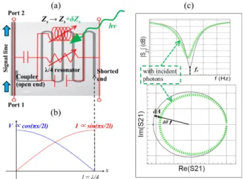
Fig. 1 (a) A photograph ofλ/4 MKID overlaid by equivalent circuit.
MKID detects incident photon through the change of surface impedance of superconducting film. (b) The distributed voltage and current in a resonator line ofλ/4 MKID. The current is maximum at the shorted end (opposite side of coupler to signal line), and hence the sensitivity is maximum at the point. (c) The magnitude (upper panel) and trajectory in complex plane (lower panel) ofS21parameter through a MKID. Black solid lines show in the dark environment, and green dot-lines indicate with photon incidence.
In practice, the power of incident photons can be measured by monitoring amplitude (A) and phase (θ) of MKID’s resonance circle.
is usually designed in microwave region of 2–8 GHz where very low-noise high electron mobility transistor (HEMT) amplifier can be used for readout. There are typically two types of MKID: having length ofλ/4, orλ/2 of readout mi- crowave. The main difference is the current distribution in a resonator line. In case ofλ/4 MKID, coupler to a signal line is open end, whereas it is shorted at the opposite side. There- fore the current density is maximum at the shorted end, and the sensitivity to incident photons is also maximum there (see Fig. 1(a) and (b)). On the other hand, the current den- sity and the sensitivity ofλ/2 MKID are maximum at the center of a resonator line since both ends are open in this case. Because of the ease of fabrication, coplanar wave guide (CPW) transmission line is a commonly used tech- nology to implement MKID on film. Figure 1(a) and (c) shows how a MKID detects incoming photons. The readout scheme is very simple: measuring transmission power of microwave (S21) through a signal line to obtain resonance frequencies (fr) and quality factors (Q) of MKIDs. When photons incident to a MKID break cooper-pairs in super- conductor, the fr and Q of the MKID change as surface impedance (Zs) of the film changes. The power of the in- cident photons can be measured by monitoring the changes of fr andQ. For practical measurement, the resonance fea- ture ofS21is a circular trajectory on a complex plane, and the changes of the fr andQcorrespond to the changes in phase (δθ) and amplitude (δA) with respect to the center of the resonance circle, respectively (see Fig. 1(c)). In the as- pect of responsivity, phase readout is about 2 times larger than the amplitude readout [19], however large excess noise is present in phase direction and it reduces the sensitivity of phase readout [20].
Since MKID is a direct photon detector sensing cooper- pair breaking, it can only detect photons with energy larger than the gap energy of superconductor (2∆), which is deter- mined by the film material. For example, 2∆of aluminium (Al) is about 0.36 meV and it corresponds to radiation of
∼90 GHz. Therefore, MKID made of Al can detect any fre- quency higher than 90 GHz, and is adequate for CMB ob- servation.
One of the most remarkable characteristics of MKID is its scalability. MKIDs can be multiplexed in frequency space (frequency division multiplex: FDMUX) asfrof each MKID can be controlled by changing the length of resonator line. FDMUX enables us to readout 100–1000 MKIDs with a single signal line, and it leads us to realize a large-format (more than 10000-pixel) camera with MKIDs using only small number of signal lines. Furthermore, MKID does not require any bias lines. These features are advantages over other large-format superconducting cameras, such as TES, in the aspect of reducing thermal flow to the coldest stage of cryostat and keeping the temperature of the coldest stage as low as possible to keep high sensitivity of superconduct- ing detector. Because of its simple structure of MKID, the fabrication process is rather simpler and one can easily earn high yield rate (more than 95%). This characteristics is also an advantage of MKID.
Taking into account these advantages, MKID cam- era for cosmological observations has been developed in cooperation of National Astronomical Observatory of Japan (NAOJ), Institute of Physical and Chemical research (RIKEN), High Energy Accelerator Research Organization (KEK), and Okayama University.
2. Development of MKID Camera
In order to develop highly sensitive MKID camera, several elemental technologies have been developed. These tech- nologies include: fabrication of high-quality Al film with Molecular Beam Epitaxy (MBE) system; development of optical components for a camera use; and development of readout circuit. The details of each development stage are described in the following subsections.
2.1 Fabrication of High-quality Film with MBE System MKID senses the number of quasi-particles (or electrons) generated when incident photons break cooper-pairs in a superconducting film. Therefore, the fundamental noise of MKID is limited by the fluctuation in the number of quasi- particles. This noise is so called generation-recombination (G–R) noise, and correspondingNEPis written as [21]:
NEPG−R=2∆ η
√ Nqp
τqp
, (1)
whereηis conversion efficiency of incident photon energy into quasi-particles [22], Nqp is number of quasi-particles, andτqp is recombination time of quasi-particles. It can be
noted that reducingNqpand extendingτqpleads to lower the NEPG−Rand increase the sensitivity of MKID. WhereasNqp
is predominantly determined by material of superconducting film, recombination time varies with the film quality such as defects or impurities in the film [23], [24].
In order to reduce defects in film, we successfully fab- ricated epitaxially-formed Al film using MBE system [25].
The Al film was deposited on a high resistivity (>15 kΩcm) Si (111) wafer in an ultra-high vacuum (UHV) chamber with pressure less than 2 × 10⁻⁷ Pa. The purity of target Al was 5 Nine. During the deposition, the film-growth rate was about 0.2–0.8 Å/s. Before the deposition, Si wafer was immersed in HF solution for cleaning of the surface. It is also annealed at 650◦ Celsius in UHV chamber to recon- struct crystal lattice structure. This step was to reduce ten- sion of interval difference of the crystalline lattice between Si and Al. The epitaxy of the Al film was confirmed by in-situ reflective high-energy electron diffraction (RHEED) and X-ray diffraction (XRD) measurements. The Residual- resistivity ratio (RRR) of fabricated Al film was about 18.
This value is larger than the RRR of Al films fabricated in different ways, such as sputtering or electron beam depo- sition, showing the high-quality of the epitaxially-formed Al film. For instance, the RRR value of electron beam de- posited Al film was measured to be about 10 at the highest [25].
The performance of the MKID made of the high- quality film was measured with cooling MKID down to 0.1 K by a dilution refrigerator. Figure 2 shows measured τqp and electricalNEPas a function of temperature mea- sured in dark environment [25].τqpwas measured from the responses in phase of MKID against LED pulses. The elec- trical NEPof MKID using phase or amplitude readout is calculated by [26]:
NEP= √ SX
(ητqp
∆ δX δNqp
)−1√
(1+ω2τ2res)(1+ω2τ2qp) (2) where X represents readout variable of phase (θ) or am- plitude (A), SX shows noise power spectral density of phase/amplitude readout, and τres = Q/(πfr) is resonator ring time. δX/δNqp denotes responsivity and is calculated as δX/δNqp = −2αQκ/V, where α is the fraction of ki- netic inductance over total inductance, and V is the vol- ume of resonator. κ = δσi/(σ2δnqp) (i = 1 for ampli- tude readout, 2 for phase readout) can be evaluated based on Mattis-Bardeen theory, withσ =σ1−iσ2 representing complex conductivity of superconductor [19]. As a result, the maximumτqp of about 450µsec with quality factor,Q, of 2×10⁶ was obtained, and very low electrical NEPof about 6×10⁻¹⁸W/√
Hz was achieved in amplitude readout with the MKID made of the high-quality Al film. Though we have demonstrated very high sensitivity of MKID, it has been proved that lower NEPcan be achieved with MKID [27]. The current sensitivity seems to be limited by stray lights [28] in our measurement system, and therefore, im- provement of readout system is underway to achieve lower NEP.
Fig. 2 Measuredτqp(blue open circles) and electricalNEP(red filled circles) of a MKID made of epitaxially-formed Al film as function of tem- perature. The thoretical curve ofτqp[29] is also shown as dot-line.
There are some remarks relating to Fig. 2. Whereas theoretical calculation shows exponential increase ofτqpby lowering temperature asτqp ∝ e∆/kBT [29] (dashed line in Fig. 2), there is a saturation ofτqpbelow 230 mK (∼ Tc/5 withTc representing critical temperature of superconduc- tor). This characteristic is quite universal for MKID made of any material, and there are several models trying to explain it [20], [24], [30]. Although the saturation limits the sen- sitivity of MKID, it can reach the fundamental noise limit even with the saturation [21], [31]. Therefore, the require- ment for the operation temperature of MKID is slightly mit- igated by virtue of the saturation, because lowering the op- eration temperature belowTc/5 does not improve the MKID sensitivity.
2.2 Development of Optical Components for MKID Cam- era
A millimeter-wave camera mainly consists of two parts:
sensor array to detect photons, and optical components (lens, antenna) to couple incoming photons to the sensors.
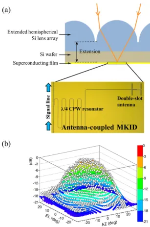
In the previous section, we described about development of sensors. Here, we focused on the development of optical components of MKID camera. We adopted lens-antenna coupled system with λ/4 MKID as a sensor. Base de- signs of antenna and lenslet are single-polarization sensitive double-slot antenna and extended hemispherical lenslet, re- spectively (see Fig. 3(a)). As the most sensitive part of a λ/4 MKID is the shorted end of a resonator, the feed point of a double-slot antenna is patterned there for effective ab- sorption of incoming photons. Incident photons are focused onto the antenna feed point by the lenslets, which are put on MKIDs’ wafer. The lenslets, made of Si, are directly machined by high-speed spindle at mechanical engineering (ME) shop of NAOJ [32]. If each lenslet is fabricated sep- arately, it needs additional efforts to mount them on corre- sponding MKIDs one by one with careful alignment. To avoid such efforts, all lenslets are machined from single polycrystal Si bulk, consisting lens array. The geometri- cal parameters of the antenna and lens array were optimized
Fig. 3 (a) Schematic drawing of optics for MKID camera developed at NAOJ. Incident lights are focused on a double slot antenna, which is pat- terned at the most sensitive part of a MKID, by extended semispherical Si lens. (b) Measured (open points) and simulated (colored filled points) beam patterns of MKID. They are in good agreement down to−15 dB level.
with 3D elecrtomagnetic field simulator, HFSS, in the fol- lowing two steps. Firstly,S11parameter of the antenna was calculated to adjust the antenna design for a target frequency and bandwidth. Then, the beam pattern of the lens-antenna system was calculated to tune the design parameters of lens array in terms of beam symmetry, side-lobe levels, and cross polarization.
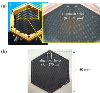
Anti-reflection (AR) coating for Si lens array was also an important topic for development. By mixing two kinds of epoxies, Stycast 1266 withn ∼1.68 and Stycast 2850FTJ withn∼2.2, we made an AR coating material with desired refractive index (n= √nS i∼1.84) [33]. The material was applied on the Si lens array and then machined along the sur- face of lens array in the desired thickness by the foremen- tioned high-speed spindle machine. Figure 4 shows 600- pixel MKIDs and Si lens array we have developed, in which lenses are allocated in closed-packed lattices. The target fre- quency of the camera is 220 GHz with bandwidth of 15%.
The diameter of each lens is∼1.64 mm, and the thickness of AR coating is about 185µm for this band. About 95%
transmittance was achieved with the AR coating [34].
Beam measurement of the designed optical system with Al MKIDs was carried out with an 0.3 K 3He sorp- tion cooler to evaluate its performance [32]. Figure 3(b) displays the measured beam pattern together with the sim-
Fig. 4 (a) Photographs of 600-pixel MKIDs. (b) A photograph of Si lens array for 600-pixel MKIDs. Anti-reflection (AR) coating is applied to the lens array. The diameters of alignment holes are 160µm and 270µm on MKID substrate and lens array, respectively. By matching the center of holes on MKID substrate and lens array, alignment accuracy of∼20µm can be achived.
ulation result. It shows good agreement between data and simulation down to−15 dB level. In order to check the per- formance of the MKID camera even for lower level of side- lobes, wider dynamic range is necessary. It can be achieved with lowering the MKID temperature, so that we designed wide field-of-view (FoV) cryogenic optical system which can be installed to our 0.1 K dilution refrigerator [35]. Note that this cryogenic optics were designed so that it can also be installed to existing radio telescopes, such as Nobeyama 45 m telescope, for astronomical observations.
2.3 Development of Readout Electronics
The simplest way to readout MKIDs is using Vector Net- work Analyzer (VNA) or homodyne detection with ana- log IQ down-converter which only reads single-tone (fre- quency) signal at a time, and covers wide frequency band by sweeping the tone frequency. However, this scheme is hardly scalable, and does not match to the requirement of fast mapping of sky†. This also does not fully take advan- tage of FDMUX capability of MKIDs as it cannot read out multiple frequencies simultaneously.
Figure 5 shows the brief schematic of readout system to fully utilize FDMUX of MKIDs. It needs an electronics which can generate and readout multiple frequency tones si- multaneously. There are two typical solutions for this: dig- ital Fast Fourier Transformation Spectrometer (FFTS) [36]
and channelized digital down conversion (DDC) technique
†For example, scan speed of GroundBIRD is 20 rpm=120◦/s.
As FoV of GroundBIRD at 150 GHz is about 0.5◦, the rate to see one sight is 120/0.5=240 Hz. Because it needs to readout about 1000 MKIDs per one sight, the readout speed of 240 kHz is the minimum requirement if reading out MKIDs one by one.
Fig. 5 Brief schematic of readout system to fully utilize FDMUX of MKIDs. Readout electronics output and readout multiple frequency tones simultaneously. In a practical readout system, several warm amplifiers, fil- ters, isolators, and attenuators are placed, but not displayed here for clarity.
[37], [38]. Each has an advantage over the other. Digital FFTS can read out 1000s of frequency tones simultaneously whereas it is about 100s at the most for DDC technique.
This is because DDC occupies more resources of Field Pro- grammable Gate Array (FPGA) equipped to the electronics.
On the other hand, DDC readout can tune each frequency of tones more freely than digital FFTS in which the interval of frequency tones are stepwise.
We developed an FFTS readout electronics with Ana- log to Digital Conveter (ADC) and Digital to Analog Converter (DAC) of 1 Gsps (sample per second) rate and 270 MHz bandwidth for MKID readout systems. It can si- multaneously generate and readout up to 4096 frequency tones with ∼61 kHz spacing. The DAC generates a set of frequency tones between 61 kHz–270 MHz from wave form data pre-programmed to memory inside the equipped FPGA. At the readout side, signals are digitized by the ADC and processed at a complex FFT module implemented in the FPGA. The processed data in the FPGA are then stored to hard disk by direct memory access (DMA) with the maxi- mum rate of 70 MB/s. Both information of amplitude and phase ofS21 can be obtained with this readout system by virtue of the implemented complex FFT. As the possible fre- quency spacing of MKID is about 1 MHz, 270 MKIDs can be ideally readout simultaneously with the developed FFTS readout. Note that we can also obtain the noise of whole measurement system except for MKID as a reference with this circuit by reading out blind frequency tones, which do not match to any resonance frequencies of MKIDs [39]. The number of possibly readout MKIDs is easily scalable by ex- tending the bandwidth of DAC and ADC used in the system.
Figure 6 shows results of noise measurement of a MKID with the developed FFTS readout circuit [40]. The measured MKID wasλ/4 resonator made of Al on Si wafer fabricated with MBE system, and cooled down to 0.1 K by dilution refrigerator††. The noise was measured in the dark environment. For a comparison, noise measurement was also carried out by combination of analog IQ down- converter and a digitizer (NI PXI-5922), which is also plot-
††These conditions are same as the experimental conditions de- scribed in Sec. 2.1.
Fig. 6 (a) The magnitude ofS21parameter of a MKID measured with analog IQ scheme (black dot-line) and FFTS circuit (red filled points). (b) The noise power spectrum densities (PSDs) of a MKID measured with ana- log IQ scheme (black dot-line) and FFTS circuit (red filled points) at read- out power of−100 dBm and temperature of 115 mK. Both noise PSDs of amplitude and phase readout are shown. The noise on phase readout is larger than amplitude readout due to so-called “Two Level System” (TLS) noise [20]. The noise floor of amplitude readout is limited by HEMT am- plifier noise. The figure shows consistent noise level between analog IQ scheme and FFTS circuit.
ted in Fig. 6. It is noticed from the figure that the developed FFTS circuit does not add any additional noise to the MKID readout system as the noise measured using FFTS system is equivalent to the noise measured using the anaolg IQ read- out scheme.
We also developed MKID readout system with DDC technique [41] with support from Open-It project of KEK.
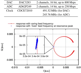
The readout electronics consists of an evaluation kit of FPGA (KC705, Xilinx Inc., USA), a digital signal processor (DSP) board (FMC150, 4DSP LLCTM, USA), and a signal generator (LMS-802, Vaunix Technology Co., USA). The FPGA and the signal generator are operated by a computer.
The DSP board, which is connected to the FPGA, has a 2- ch DAC, 2-ch ADC and clock chip (Table 1). The DAC generates up to 32 frequency tones simultaneously. The fre- quencies of them can be selected in multiples of 12.288 kHz between 3–82 MHz by the computer control. The tones are up-converted using the signal generator, and provided to MKIDs. The return signals are digitized by the ADC after down-converting. It is demodulated by each tone in FPGA. The processed data (12.288 ksps) was transferred to the computer using Ethernet connection by SiTCP [42].
As a demonstration, we measured a MKID response using the DDC readout circuit. The MKID is cooled down to 0.25 K by a sorption cooler in the dark environment. Fig- ure 7 shows results of the response.
3. Calibration of Optical Responsivity
For the precise CMB polarization observation experiment, the calibration of the detector in the realistic environment at
Table 1 List of integrated circuit chips equipped on the DSP daughter board.
DAC DAC3283 2 channels, 16 bit, up to 800 Msps ADC AD62P249 2 channels, 14 bit, up to 250 Msps Clock CDCE72010 491.52 MHz (for DAC)
245.76 MHz (for ADC)
Fig. 7 Response of MKID inIQ-plane, whereIandQcorrespond to Real(S21) and Imag(S21) in Fig. 1, respectively. Cross markers show aver- ages in 0.7 sec at each frequency. Circle markers show the response with fixed feed frequency at the resonance peak for 100 sec. Each point is an average of 1000 samples. MKID should have responce for the variation of magnetic fields. Variation of the plots comes from the magnetic fields’s modulation.
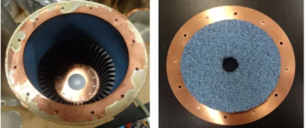
a laboratory is crucial. To realize such environment, we have developed a calibration system with the modulated polariza- tion source in a dilution cryostat whose minimum tempera- ture reaches down to 100 mK. Figure 8 shows the schematic of the constructed calibration system named “Polarization Signal Simulator” [43]. It consists of a rotational metal- lic mirror at 115 K and the blackbody emitter at 4.5 K in the cryostat. The mirror emits a polarization signal, and is mounted so as to be inclined at 45◦ to the line of sight to the detector (Fig. 9). In this configuration, the mirror causes weak polarized light because of the difference of the emissivity of the p-polarized and s-polarized lights to the detector. The blackbody emitters are mounted on the in- ner side of the 4.5 K thermal shield. The emitter consists of 616 pyramid-shaped grooves so as to achieve the black- body radiation (Fig. 10). Each groove is fabricated by using an Al core on which the radio absorber, Eccosorb CR-1128, is casted. Eccosorb CR-1128 is an iron-loaded epoxy from Emerson & Cuming Microwave Products, Inc. Each groove has the square base of 64 mm2and height of 18 mm. PTFE and nylon 6/6 thermal filters are inserted between the mirror and the detector to reduce the blackbody component above
∼500 GHz [44], [45]. The transmission efficiency of the fil- ters were 0.8 in total at 220 GHz.
The generated polarization signal consists of the emis- sion from the mirror surface at 115 K and the reflection of the blackbody emission from the pyramid-shaped grooves at 4.5 K. The magnitude of the p-polarization power expressed in temperature is calculated by
P=2√πνρε0tanβ(Tmirror−Tbb). (3)
Fig. 8 Schematic of Polarization Signal Simulator.
Fig. 9 Photograph of the polarization mirror made by SUS-316L.
Fig. 10 The left picture shows the blackbody emitter inside the 4.5 K thermal shield. 616 pyramid-shaped grooves are mounted on the inner wall of the shield. The vacant area on the inner wall is covered by the flat Ec- cosorb. The right picture shows the cap of the 4K shield. The inner wall is also coverd by the flat Eccosorb.
whereν,ρ,βandε0are the observed frequency, the resis- tivity of the rotation mirror, the inclination angle of the mir- ror and the vacuum permittivity, respectively, andTmirrorand Tbbare the temperatures of the rotation mirror and the black- body grooves. Here, the net intensity of the polarization is proportional toTmirror−Tbbbecause the net polarization of both components is perpendicular to each other. The cal- culated power in temperature as a function of frequency is shown in Fig. 11 for the SUS-316L and Al, respectively.
We have performed the evaluation of the polarization sensitivity of an Al 3×3 MKIDs by using this simulator.
The MKIDs were fabricated by using an Al film deposited by MBE system (see Sec. 2.1). The planar antennas coupled
Fig. 11 Polarization intensity in temperature of the aluminum and SUS- 316L mirrors.
to MKIDs were optimized for 220 GHz with bandwidth of 15%. Si lens array was set on the back side of the MKIDs as described in Sec. 2.2. The observed quality factors (Q) ranged from Q = (1.9 −8.2) ×104, which were a few times lower than without the simulator due to higher loading power. The real-time signal readout was performed by us- ing the DDC readout system described in Sec 2.3 by which both the amplitude and phase signals were observed for each MKID.
The noise equivalent temperature (NET) is expressed by
NET =( 1/√
2)
×P×Sθ/Aθ (4) wherePis the input power in temperature at 220 GHz,Sθ is the noise spectrum in phase, and Aθis the amplitude of the modulated intensity of the polarized phase signal along with the mirror rotation. This expression means that NET can be directly derived by the input power in temperature di- vided by the measured signal-to-noise ratio (Aθ/Sθ). These derivedNET values are independent of the detector param- eters such as the quality factor, Q, and the recombination time,τqp, as well as the optical setup at the 100 mK stage.
In this evaluation, the power of 400 mK was derived from Fig. 11 at 220 GHz, and the transmittance of the ther- mal filter of 0.8 at 220 GHz was used. Then, P was esti- mated to be 320 mK.Aθwas derived by using the modula- tion signal amplitude of the phase with the mirror rotation.
The example of the actual observed signal was shown in Fig. 12. In all nine signals, two component modulated with rotation were observed. One component (shown as “1f”) has modulated at the rotation frequency, f, and another one (shown as “2f”) at the twice of the rotation frequency. We have confirmed that the most of the modulation in the 2f signal was due to the polarization rotation because the mod- ulation phase relative to the 1f signal has theπ/2 difference for the antennas with the || and =polarization directions.
The evaluatedNET values are summarized in Table 2. The values range in 190–750µK√
sat the sampling frequency of 100 Hz [45]. These values are comparable to the values in the BICEP2 experiment (300µK√
s) which is the best po- larization sensitivity reported so far [11].
Fig. 12 Example of the obtained phase signal. Red line shows the total obtained component. Green and blue lines indicate the components mod- ulated with the rotation frequency and the twice frequency of the mirror, respectively.
Table 2 The derivedNETand opticalNEPof MKIDs.
No. Antenna direction NET[µK√s] OpticalNEP[W/√ Hz]
A || 270 1.6×10⁻¹⁶
B = 310 1.8×10⁻¹⁶
C = 370 2.1×10⁻¹⁶
D || 310 1.8×10⁻¹⁶
E || 190 1.1×10⁻¹⁶
F = 550 3.2×10⁻¹⁶
G = 750 4.4×10⁻¹⁶
H || 750 4.4×10⁻¹⁶
I || 460 2.7×10⁻¹⁶
The obtainedNETvalues can be translated into the op- ticalNEPassuming the band width,dν, of the detectors by using the formula:
NEP= √
2kBdν×NET. (5)
From this formula, opticalNEPvalues are also estimated as shown in Table 2 which range from (1.1 − 4.4) × 10−16 W/√
Hz [45]. Since the optical loading in this ex- perimental setup was∼100 pW, the results showed that our MKID camera almost reached the photon noise level at that loading power [46]. These opticalNEPs are sufficiently low for a ground-based CMB observation. However, it is still not enough for a satellite mission. The next step of our devel- opment is to improve the performance of MKID camera for use in a space-based CMB observation.
4. Conclusion
MKID is a highly sensitive superconducting detector, of which potential is currently well-recognized and the devel- opment is actively proceeded all over the world. MKID camera for cosmological observations has been developed in cooperation of NAOJ, RIKEN, KEK, and Okayama Uni- versity. The developments include several elemental tech- nologies: fabrication of high-quality film; optical compo- nents for a camera use; high-speed and wide-band readout circuit using frequency tones; and calibration system incor- porated in a cooling system. These technologies are also
common for general superconducting camera. We believe that our developments not only contribute to future cosmo- logical observations, but also lead to the further progress in the development of superconducting detectors.
Acknowledgments
This work was supported by Grants-in-Aid for Scientific Research from The Ministry of Education, Culture, Sports, Science, and Technology, Japan (KAKENHI Grant Num- ber 21111003, 21244023, 24111712, 25247022, 23684017, and 26247045). It was also supported by the Center for the Promotion of Integrated Sciences (CPIS) of SOK- ENDAI, and the Basic Science Research Program through the National Research Foundation of Korea (NRF) funded by the Ministry of Education, Science and Technology (2013R1A1A2004972).
References
[1] A. A. Penzias and R. W. Wilson, “A measurement of excess antenna temperature at 4080 Mc/s,” Astrophys. J., vol.142, pp.419–421, July 1965.
[2] G. Hinshaw, D. Larson, E. Komatsu, D. N. Spergel, C. L. Bennett, J. Dunkley, M. R. Nolta, M. Halpern, R. S. Hill, N. Odegard, L.
Page, K. M. Smith, J. L. Weiland, B. Gold, N. Jarosik, A. Kogut, M. Limon, S. S. Meyer, G. S. Tucker, E. Wollack, and E. L. Wright,
“Nine-yearWilkinson Microwave Anisotropy Probe(WMAP) obser- vations: Cosmological parameter results,” Astrophys. J. Suppl. Ser., vol.208, no.2, pp.19, Oct. 2013.
[3] Planck Collaboration, P. Ade, et al., “Planck 2013 results. XVI. Cos- mological parameters,” 2013.
[4] K. Sato, “First order phase transition of a vacuum and expansion of the universe,” Mon. Not. R. Astron. Soc., vol.195, no.3, pp.467–479, July 1981.
[5] A. H. Guth, “The inflationary universe: A possible solution to the horizon and flatness problems,” Phys. Rev. D, vol.23, no.2, pp.347–
356, Jan. 1981.
[6] Planck Collaboration, P. Ade, et al., “Planck 2013 results. XXII.
Constraints on inflation,” 2013.
[7] U. Seljak and M. Zaldarriaga, “Signature of gravity waves in po- larization of the microwave background,” Phys. Rev. Lett., vol.78, no.11, pp.2054–2057, Mar. 1997.
[8] M. Kamionkowski, A. Kosowsky, and A. Stebbins, “A probe of pri- mordial gravity waves and vorticity,” Phys. Rev. Lett., vol.78, no.11, pp.2058–2061, Mar. 1997.
[9] M. Zaldarriaga and U. Seljak, “All-sky analysis of polarization in the microwave background,” Phys. Rev. D Part. Fields, vol.55, no.4, pp.1830–1840, Feb. 1997.
[10] M. Kamionkowski, A. Kosowsky, and A. Stebbins, “Statistics of cosmic microwave background polarization,” Phys. Rev. D, vol.55, no.12, pp.7368–7388, June 1997.
[11] P. A. Ade, R. W. Aikin, D. Barkats, S. J. Benton, C. A. Bischoff, J. J.
Bock, J. A. Brevik, I. Buder, E. Bullock, C. D. Dowell, L. Duband, J. P. Filippini, S. Fliescher, S. R. Golwala, M. Halpern, M. Has- selfield, S. R. Hildebrandt, G. C. Hilton, V. V. Hristov, K. D. Irwin, K. S. Karkare, J. P. Kaufman, B. G. Keating, S. A. Kernasovskiy, J. M. Kovac, C. L. Kuo, E. M. Leitch, M. Lueker, P. Mason, C. B.
Netterfield, H. T. Nguyen, R. O’Brient, R. W. Ogburn 4th, A. Or- lando, C. Pryke, C. D. Reintsema, S. Richter, R. Schwarz, C. D.
Sheehy, Z. K. Staniszewski, R. V. Sudiwala, G. P. Teply, J. E. Tolan, A. D. Turner, A. G. Vieregg, C. L. Wong, and K. W. Yoon; BICEP2 Collaboration, “Detection ofB-mode polarization at degree angular scales by BICEP2,” Phys. Rev. Lett., vol.112, no.24, pp.241101-1–
241101-25, June 2014.
[12] O. Tajima, J. Choi, M. Hazumi, H. Ishitsuka, M. Kawai, and M.
Yoshida, “GroundBIRD: An experiment for CMB polarization mea- surements at a large angular scale from the ground,” Proc. SPIE, vol.8452, pp.84521M, 2012.
[13] M. Hazumi, J. Borrill, Y. Chinone, M. A. Dobbs, H. Fuke, A. Ghribi, M. Hasegawa, K. Hattori, M. Hattori, W. L. Holzapfel, Y. Inoue, K. Ishidoshiro, H. Ishino, K. Karatsu, N. Katayama, I. Kawano, A.
Kibayashi, Y. Kibe, N. Kimura, K. Koga, E. Komatsu, A. T. Lee, H. Matsuhara, T. Matsumura, S. Mima, K. Mitsuda, H. Morii, S.
Murayama, M. Nagai, R. Nagata, S. Nakamura, K. Natsume, H.
Nishino, A. Noda, T. Noguchi, I. Ohta, C. Otani, P. L. Richards, S. Sakai, N. Sato, Y. Sato, Y. Sekimoto, A. Shimizu, K. Shinozaki, H. Sugita, A. Suzuki, T. Suzuki, O. Tajima, S. Takada, Y. Takagi, Y. Takei, T. Tomaru, Y. Uzawa, H. Watanabe, N. Yamasaki, M.
Yoshida, T. Yoshida, and K. Yotsumoto, “LiteBIRD: A small satel- lite for the study of B-mode polarization and inflation from cosmic background radiation detection,” Proc. SPIE, vol.8442, pp.844219, 2012.
[14] T. Matsumura, Y. Akiba, J. Borrill, Y. Chinone, M. Dobbs, H.
Fuke, A. Ghribi, M. Hasegawa, K. Hattori, M. Hattori, M. Hazumi, W. Holzapfel, Y. Inoue, K. Ishidoshiro, H. Ishino, H. Ishitsuka, K. Karatsu, N. Katayama, I. Kawano, A. Kibayashi, Y. Kibe, K.
Kimura, N. Kimura, K. Koga, M. Kozu, E. Komatsu, A. Lee, H.
Matsuhara, S. Mima, K. Mitsuda, K. Mizukami, H. Morii, T. Mori- shima, S. Murayama, M. Nagai, R. Nagata, S. Nakamura, M.
Naruse, K. Natsume, T. Nishibori, H. Nishino, A. Noda, T. Noguchi, H. Ogawa, S. Oguri, I. Ohta, C. Otani, P. Richards, S. Sakai, N.
Sato, Y. Sato, Y. Sekimoto, A. Shimizu, K. Shinozaki, H. Sugita, T.
Suzuki, A. Suzuki, O. Tajima, S. Takada, S. Takakura, Y. Takei, T.
Tomaru, Y. Uzawa, T. Wada, H. Watanabe, M. Yoshida, N. Yama- saki, T. Yoshida, and K. Yotsumoto, “Mission design of LiteBIRD,”
J. Low Temp. Phys., vol.176, no.5–6, pp.733–740, Sept. 2014.
[15] N. Katayama and E. Komatsu, “Simple foreground cleaning algo- rithm for detecting primordialB-mode polarization of the cosmic microwave background,” Astrophys. J., vol.737, no.2, pp.78, Aug.
2011.
[16] K. D. Irwin, “An application of electrothermal feedback for high resolution cryogenic particle detection,” Appl. Phys. Lett., vol.66, no.15, pp.1998–2000, Apr. 1995.
[17] P. K. Day, H. G. LeDuc, B. A. Mazin, A. Vayonakis, and J. Zmuidzi- nas, “A broadband superconducting detector suitable for use in large arrays,” Nature, vol.425, no.6960, pp.817–821, Oct. 2003.
[18] J. Zmuidzinas, “Superconducting microresonators: Physics and ap- plications,” Annu. Rev. Cond. Mat. Phys., vol.3, pp.169–214, Mar.
2012.
[19] J. Gao, The Physics of Superconducting Microwave Resonators, Ph.
D. thesis, California Institute of Technology, 2006.
[20] J. Gao, J. Zmuidzinas, B. A. Mazin, H. G. LeDuc, and P. K.
Day, “Noise properties of superconducting coplanar waveguide mi- crowave resonators,” Appl. Phys. Lett., vol.90, no.10, pp.102507, Mar. 2007.
[21] S. J. C. Yates, J. J. A. Baselmans, A. Endo, R. M. J. Janssen, L. Fer- rari, P. Diener, and A. M. Baryshev, “Photon noise limited radiation detection with lens-antenna coupled microwave kinetic inductance detectors,” Appl. Phys. Lett., vol.99, no.7, pp.073505, Aug. 2011.
[22] A. G. Kozorezov, A. F. Volkov, J. K. Wigmore, A. Peacock, A. Poe- laert, and R. den Hartog, “Quasiparticle-phonon downconversion in nonequilibrium superconductors,” Phys. Rev. B, vol.61, no.17, pp.11807–11819, May 2000.
[23] R. Barends, S. van Vliet, J. J. A. Baselmans, S. J. C. Yates, J. R. Gao, and T. M. Klapwijk, “Enhancement of quasiparticle recombination in Ta and Al superconductors by implantation of magnetic and non- magnetic atoms,” Phys. Rev. B, vol.79, no.2, pp.020509, Jan. 2009.
[24] T. Noguchi, M. Naruse, and Y. Sekimoto, “Contribution of quasi- particles in the subgap states to the surface impedance of supercon- ductors,” IEEE Trans. Appl. Supercond., vol.23, no.3, pp.1501404,
June 2013.
[25] M. Naruse, Y. Sekimoto, T. Noguchi, A. Miyachi, T. Nitta, and Y.
Uzawa, “Development of crystal Al MKIDs by molecular beam epi- taxy,” J. Low Temp. Phys., vol.167, no.3–4, pp.373–378, May 2012.
[26] B. A. Mazin, Microwave Kinetic Inductance Detectors, Ph.D. thesis, California Institute of Technology, 2004.
[27] P. de Visser, J. J. A. Baselmans, P. Diener, S. J. C. Yates, A. Endo, and T. Klapwijk, “Generation-recombination noise: The fundamen- tal sensitivity limit for kinetic inductance detectors,” J. Low Temp.
Phys., vol.167, no.3–4, pp.335–340, May 2012.
[28] J. J. A. Baselmans, S. J. C. Yates, “Long quasiparticle lifetime in Aluminum Microwave Kinetic Inductance Detectors using coaxial stray light filters,” AIP Conf. Proc., vol.1185, no.1, pp.160–163, 2009.
[29] S. B. Kaplan, C. C. Chi, D. N. Langenberg, J. J. Chang, S. Jafarey, and D. J. Scalapino, “Quasiparticle and phonon lifetimes in super- conductors,” Phys. Rev. B, vol.14, no.11, pp.4854–4873, Dec. 1976.
[30] P. de Visser, D. J. Goldie, P. Diener, S. Withington, J. J. A. Basel- mans, and T. M. Klapwijk, “Evidence of a nonequilibrium distribu- tion of quasiparticles in the microwave response of a superconduct- ing aluminum resonator,” Phys. Rev. Lett., vol.112, no.4, pp.047004, Jan. 2014.
[31] R. M. J. Janssen, J. J. A. Baselmans, A. Endo, L. Ferrari, S. J. C.
Yates, A. M. Baryshev, and T. M. Klapwijk, “High optical efficiency and photon noise limited sensitivity of microwave kinetic inductance detectors using phase readout,” Appl. Phys. Lett., vol.103, no.20, pp.203503, Nov. 2013.
[32] T. Nitta, M. Naruse, Y. Sekimoto, K. Mitsui, N. Okada, K. Karatsu, M. Sekine, H. Matsuo, T. Noguchi, Y. Uzawa, M. Seta, and N.
Nakai, “Beam pattern measurements of millimeter-wave kinetic in- ductance detector camera with direct machined silicon lens array,”
IEEE Trans. Terahertz Sci. Technol., vol.3, no.1, pp.56–62, Jan.
2013.
[33] T. Nitta, S. Sekiguchi, Y. Sekimoto, K. Mitsui, N. Okada, K.
Karatsu, M. Naruse, M. Sekine, H. Matsuo, T. Noguchi, M. Seta, and N. Nakai, “Anti-reflection coating for cryogenic silicon and alu- mina lenses in millimeter-wave bands,” J. Low Temp. Phys., vol.176, no.5–6, pp.677–683, Sept. 2014.
[34] T. Nitta, K. Karatsu, Y. Sekimoto, M. Naruse, M. Sekine, S.
Sekiguchi, H. Matsuo, T. Noguchi, K. Mitsui, N. Okada, M. Seta, and N. Nakai, “Close-packed silicon lens antennas for millimeter- wave MKID camera,” J. Low Temp. Phys., vol.176, no.5–6, pp.684–
690, Sept. 2014.
[35] S. Sekiguchi, et al., “Development of the wide FoV cold optics for millimeter and submillimeter wave observation,” The 25th Interna- tional Symposium on Space Terahertz Technology, Apr. 2014.
[36] S. J. C. Yates, A. M. Baryshev, J. J. A. Baselmans, B. Klein, and R. Güsten, “Fast fourier transform spectrometer readout for large arrays of microwave kinetic inductance detectors,” Appl. Phys. Lett., vol.95, no.4, pp.042504, July 2009.
[37] O. Bourrion, A. Bideaud, A. Benoit, A. Cruciani, J. F. Macias-Perez, A. Monfardini, M. Roesch, L. Swenson, and C. Vescovi, “Electron- ics and data acquisition demonstrator for a kinetic inductance cam- era,” J. Inst., vol.6, pp.P06012, June 2011.
[38] S. McHugh, B. A. Mazin, B. Serfass, S. Meeker, K. O’Brien, R.
Duan, R. Raffanti, and D. Werthimer, “A readout for large arrays of microwave kinetic inductance detectors,” Rev. Sci. Instrum., vol.83, no.4, pp.044702, Apr. 2012.
[39] S. J. C. Yates, J. J. A. Baselmans, A. M. Baryshev, Y. J. Y. Lankwar- den, L. Swenson, A. Monfardini, B. Klein, R. Gusten, B. Young, B. Cabrera, and A. Miller, “Readout for large arrays of microwave kinetic inductance detectors using a fast fourier transform spectrom- eter,” AIP Conf. Proc., vol.1185, no.1, pp.249–252, 2009.
[40] K. Karatsu, M. Naruse, T. Nitta, M. Sekine, S. Sekiguchi, Y. Seki- moto, T. Noguchi, Y. Uzawa, H. Matsuo, and H. Kiuchi, “Measure- ment of MKID performance with high-speed and wide-band readout system,” J. Low Temp. Phys., vol.176, no.3–4, pp.459–464, Aug.
2014.
[41] K. Hattori, M. Hazumi, H. Ishino, A. Kibayashi, Y. Kibe, S. Mima, T. Okamura, N. Sato, T. Tomaru, Y. Yamada, M. Yoshida, T. Yuasa, and H. Watanabe, “Development of microwave kinetic inductance detectors and their readout system for litebird,” Nucl. Instrum. Meth.
A, vol.732, no.0, pp.306–310, 2013. Vienna Conference on Instru- mentation 2013.
[42] T. Uchida, “Hardware-based TCP processor for Gigabit ethernet,”
IEEE Trans. Nucl. Sci., vol.55, no.3, pp.1631–1637, June 2008.
[43] K. Takahashi, S. Mima, S. Oguri, C. Otani, O. Tajima, H. Watanabe, and M. Yoshida, “Calibration system with modulated polarization source for superconducting detectors at 0.1K,” J. Low Temp. Phys., vol.176, no.5–6, pp.822–828, Sept. 2014.
[44] M. Hasegawa, O. Tajima, Y. Chinone, M. Hazumi, K. Ishidoshiro, and M. Nagai, “Calibration system with cryogenically-cooled loads for cosmic microwave background polarization detectors,” Rev. Sci.
Instrum., vol.82, no.5, pp.054501, May 2011.
[45] K. Takahashi, Ph.D. thesis, Tohoku University, 2014.
[46] M. Naruse, Y. Sekimoto, T. Noguchi, A. Miyachi, K. Karatsu, T.
Nitta, M. Sekine, Y. Uzawa, T. Taino, and H. Myoren, “Optical effi- ciencies of lens-antenna coupled kinetic inductance detectors at 220 GHz,” IEEE Trans. Terahertz Sci. and Technol., vol.3, no.2, pp.180–
186, Mar. 2013.
Kenichi Karatsu received a PhD degree in science from Kyoto University in 2011. Ad- vanced Technology Center (ATC) of National Astronomical Observatory of Japan (NAOJ), 2- 21-1 Osawa, Mitaka, Tokyo, 181-8588 Japan.
Satoru Mima received a Ph.D. degree in sci- ence from Okayama University in 2013. Since 2012, he is a researcher of THz Sensing and Imaging Team of RIKEN.
Shugo Oguri received a PhD degree in sci- ence from the University of Tokyo in 2012. In- stitute of Particle and Nuclear Studies, High En- ergy Accelerator Research Organization (KEK), 1-1 Oho, Tsukuba, Ibaraki, 305-0801 Japan.
Jihoon Choi received a M.S. degree in science from Korea University in 2005. De- partment of Physics Korea University, Anam 5-1, Seongbuk, Seoul 136-713, Republic of Korea.
R. M. Thushara Damayanthi received a Ph.D. degree in Engineering from Graduate School of Engineering, University of Tokyo in 2009. Since 2013, she is a researcher of THz Sensing and Imaging Team of RIKEN.
Agnes Dominjon received a PhD degree in science from the University of Savoy (France) in 1996. She is a French assistant professor de- tached on a research position at Advanced Tech- nology Center (ATC) of National Astronomical Observatory of Japan (NAOJ), 2-21-1 Osawa, Mitaka, Tokyo, 181-8588 Japan.
Noboru Furukawa received a master of engineering degree from Waseda University in 1974. He is a technical staffof THz Sensing and Imaging Team of RIKEN.
Hirokazu Ishino received a PhD degree in Science from the University of Tokyo in 1999.
Graduate School of Natural Science and Tech- nology, Okayama University, 3-1-1, Tsushima- naka, Kita-ku, Okayama, 700-8530 Japan.
Hikaru Ishitsuka Department of Particle and Nuclear Physics, School of High Energy Accelerator Science, The Graduate University for Advanced Studies (SOKENDAI), Shonan Village, Hayama, Kanagawa 240-0193 Japan.
Atsuko Kibayashi received a PhD degree in Physics from University of Hawaii in 2002.
Graduate School of Natural Science and Tech- nology, Okayama University, 3-1-1, Tsushima- naka, Kita-ku, Okayama, 700-8530 Japan.
Yoshiaki Kibe received a PhD degree in sci- ence from Tohoku University in 2010. Nagoya Proton Therapy Center, Nagoya City West Med- ical Center, 1-1-1 Hirate-cho, Kita-ku, Nagoya, 462-8508 Japan.
Hitoshi Kiuchi received the B.E. and Ph.D.
degrees in electronic engineering from univer- sity of electro-communications, Tokyo, Japan, in 1982 and 2001, respectively. In 1982, he joined the Radio Research Laboratory, Ministry of Posts and Telecommunications (now the Na- tional Institute of Information and Communica- tions Technology), Tokyo, Japan. He was in charge of VLBI (very long baseline interferome- ter), especially a correlation processing system, a data-acquisition system and a reference fre- quency system. In 2004, he joined the National Astronomical Observatory in Japan. Since then his research activity is concerned with a photonic local system/a THz source for ALMA (Atacama Large Millimeter/submillimeter Array) radio interferometer and a read-out system for MKIDS.
Kensuke Koga received a M. S. degree in astronomy from Tohoku University in 2010.
From 2014, he has been working at NuFlare Technology, Inc. (NFT) in Japan.
Masato Naruse received a PhD degree in science from the University of Tokyo in 2012. Graduate School of Science and Technol- ogy of Saitama University, 255 Shimo-Ohkubo, Sakura-ku, Saitama, Saitama, 338-8570 Japan.
Tom Nitta received a PhD degree in sci- ence from University of Tsukuba in 2014. Ad- vanced Technology Center (ATC) of National Astronomical Observatory of Japan (NAOJ), 2-21-1 Osawa, Mitaka, Tokyo, 181-8588 Japan.
Takashi Noguchi was born in Saitama, Japan in 1952. He received the B.S., M.S.
and Ph.D. degrees in applied physics from Tohoku University, Sendai, Japan, in 1976, 1978 and 1981, respectively. In 1981, he joined the Central Research Laboratory, Mitsubishi Electric Corporation, where he was engaged in the research and development of superconduct- ing devices for analog applications. He left Mitsubishi Electric Corporation in 1991 to join National Astronomical Observatory of Japan, where he worked on research and development of low-noise SIS mixers for millimeter- and submillimeter-wave receivers. Now he is in charge of development and production of SIS junctions for millimeter- and submillimeter-wave receivers of ALMA. His current research interest is the development of high-sensitivity superconductive detectors at submilli- meter wavelengths. Advanced Technology Center, National Astronomical Observatory of Japan, 2-21-1 Osawa, Mitaka, Tokyo, 181-8588 Japan.
Takashi Okada is a graduate school student at the University of Tokyo. Advanced Tech- nology Center (ATC) of National Astronomical Observatory of Japan (NAOJ), 2-21-1 Osawa, Mitaka, Tokyo, 181-8588 Japan.
Chiko Otani received his Ph.D. degree in astronomy from University of Tokyo in 1995.
Since 2005, he is a team leader of THz Sensing and Imaging Team of RIKEN.
Shigeyuki Sekiguchi is a graduate school student at the University of Tokyo. Advanced Technology Center (ATC) of National Astro- nomical Observatory of Japan (NAOJ), 2-21-1 Osawa, Mitaka, Tokyo, 181-8588 Japan.
Yutaro Sekimoto is an associated professor at Advanced Technology Center, National As- tronomical Observatory of Japan. He received his PhD degree in physics from the University of Tokyo in 1994.
Masakazu Sekine is a graduate school student at the University of Tokyo. Advanced Technology Center (ATC) of National Astro- nomical Observatory of Japan (NAOJ), 2-21-1 Osawa, Mitaka, Tokyo, 181-8588 Japan.
Shibo Shu is a graduate school student at the University of Tokyo. Advanced Technology Center (ATC) of National Astronomical Obser- vatory of Japan (NAOJ), 2-21-1 Osawa, Mitaka, Tokyo, 181-8588 Japan.
Osamu Tajima received a PhD degree in science from Tohoku University in 2003. Insti- tute of Particle and Nuclear Studies, High En- ergy Accelerator Research Organization (KEK), 1-1 Oho, Tsukuba, Ibaraki, 305-0801 Japan.
Kenta Takahashi received a Ph.D. degree in physics from Tohoku University in 2014, re- spectively. From 2014, he has been working at Harmonic Drive Systems Inc. in Japan.
Nozomu Tomita received a master degree in science degree from the University of Tokyo in 2014. The university of Tokyo, 7-3-1 Hongo, Bunkyo-ku, Tokyo, 113-0033 Japan.
Hiroki Watanabe Department of Particle and Nuclear Physics, School of High Energy Accelerator Science, The Graduate University for Advanced Studies (SOKENDAI), Shonan Village, Hayama, Kanagawa 240-0193 Japan.
Mitsuhiro Yoshida received a Ph.D. de- gree in science from the University of Tokyo in 2004. Accelerator Division, High Energy Accelerator Research Organization (KEK), 1-1 Oho, Tsukuba, Ibaraki, 305-0801 Japan.