Koji TAKEDA
†a), Tomonari SATO
†, Nonmembers, Takaaki KAKITSUKA
†, Member, Akihiko SHINYA
††, Kengo NOZAKI
††, Chin-Hui CHEN
†, Hideaki TANIYAMA
††, Masaya NOTOMI
††, Nonmembers, and Shinji MATSUO
†, Member
SUMMARY To meet the demand for light sources for on-chip opti- cal interconnections, we demonstrate the continuous-wave (CW) operation of photonic-crystal (PhC) nanocavity lasers at up to 89.8◦C by using InP buried heterostructures (BH). The wavelength of a PhC laser can be pre- cisely designed over a wide range exceeding 100 nm by controlling the lat- tice constant of the PhC. The dynamic responses of the PhC laser are also demonstrated with a 3-dB bandwidth of over 7.0 GHz at 66.2◦C. These re- sults reveal the laser’s availability for application to wavelength division multiplexed (WDM) optical interconnection on CMOS chips. We discuss the total bandwidths of future on-chip optical interconnections, and report the capabilities of PhC lasers.
key words: photonic-crystal lasers, buried heterostructures, optical inter- connections
1. Introduction
The size of Si CMOS devices is continually being reduced to increase their speed, and so interconnections in CMOS chips now account for more than half of the total power con- sumption [1]. On-chip optical interconnections have been widely studied and developed to overcome the trade-o ff be- tween operating speed and power consumption [2]; attempts have been made to reduce the power consumption of inter- connections and simultaneously improve their bandwidth.
There are certain requirements for optical devices designed for use in practical on-chip optical interconnections: (1) a total bandwidth of 1 Tb/s [3], (2) high-temperature opera- tion up to 80
◦C [3], and (3) an energy consumption of less than 10 fJ/bit [4]. The first requirement makes wavelength- division multiplexing (WDM) essential, since no optical communication has been demonstrated at over 1 Tb/s per channel. Wavelength controllability is an important param- eter as regards using optical devices for WDM. The sec- ond feature relates to the surface temperatures of typical CMOS LSIs. The third requirement originates with the lim- ited power dissipation of each CMOS chip. It is important to reduce the active-region volumes of lasers if we are to reduce their energy costs.
Therefore, nanocavity lasers are required as light sources for on-chip optical interconnections [5]. Of the sev- eral types of nanocavity lasers, photonic-crystal (PhC) lasers
Manuscript received November 10, 2011.
Manuscript revised March 6, 2012.
†
The authors are with NTT Photonics Laboratories, NTT Cor- poration, Atsugi-shi, 243-0198 Japan.
††
The authors are with NTT Basic Research Laboratories, NTT Corporation, Atsugi-shi, 243-0198 Japan.
a) E-mail: [email protected] DOI: 10.1587/transele.E95.C.1244
are being actively studied [6]–[9], since their mode volumes are one order smaller than those of vertical-cavity surface- emitting lasers (VCSELs) [10], [11], and their output pow- ers are larger than those of metallic nanocavity lasers [12], [13]. However, it is di ffi cult for PhC lasers to achieve both a small volume and high temperature operation, because they have a large thermal resistance resulting from the strong light confinement between semiconductors and air that is achieved by using a high-index contrast. There have been few reports on the high-temperature operation of PhC lasers [14], and no reports have yet reported operation under a continuous-wave (CW) condition.
We have also developed a PhC laser with an ultra-small active region buried in an InP line-defect waveguide, and demonstrated a low energy cost of 8.8 fJ/bit at a data rate of 20 Gb / s. Although the device has met the energy consump- tion requirement, high-temperature or wavelength designs have not yet been studied.
In this paper, we demonstrate the CW, 89.8
◦C oper- ation of PhC lasers as well as their availability for on-chip WDM networks. Wavelengths can be controlled with ±1 nm accuracy over a 100-nm range. The dynamic responses of the PhC laser are also demonstrated at room temperature (RT) and 66.2
◦C, and 3-dB bandwidths of 11.6 and 7.0 GHz are realized. We discuss the total bandwidth of future on- chip optical interconnections, and describe the possibility of a total bandwidth of 1 Tb/s.
2. Device Structure
Figure 1(a) shows a cross-sectional SEM image of a PhC laser. Ultra-small 3-quantum-well (QW) active layers, which have a photoluminescence peak at 1.55 µm, are em- bedded in a line-defect PhC waveguide consisting of a 200- nm-thick InP membrane using butt-joint technologies. The active region is 5 × 0.3 × 0.15 µm
3. The barrier layers of the QW are InGaAsP with a photoluminescence peak of 1.35 µm (1.35Q).
Line-defect PhC waveguides are defined on the InP
membranes as shown in Fig. 1(b). The center waveguide is
used for a pump light. The lasing light is coupled to the out-
put waveguide, which is located in the Γ -M direction from
the active region. We confine the light in the active region
by a photonic bandgap effect and an energy shift of the even
mode along the photonic crystal waveguide [15]. The pho-
tonic band diagram is shown in Fig. 2. A gap between the
Copyright c 2012 The Institute of Electronics, Information and Communication Engineers
Fig. 1 Scanning electron microscope (SEM) images of (a) a cross sec- tion and (b) a top view of a buried-heterostructure (BH) PhC laser. A 3-QW active region is embedded in the InP membrane using butt-joint technolo- gies. The center waveguide is used as a pumping waveguide. A line-defect waveguide for the output light is located in theΓ-M direction from the ac- tive region.
Fig. 2 Photonic band diagram of the photonic crystal waveguide. Blue and red solid lines correspond to the dispersion curves with and without the active region. A gap between red and blue curve within the green hatched region, which shows a photonic bandgap, creates the cavity mode.
blue (without the active region) and the red (with the active region) solid line creates the cavity mode. The lattice con- stant of the PhC is varied from 410 to 440 nm. The hole diameter is designed to be 200 nm.
Fig. 3 Schematic of measurement setup.
Fig. 4 Lasing wavelength versus lattice constant of the PhC. A wave- length range of 100 nm was obtained with the PhC lasers by changing the lattice constant from 410 to 440 nm. The wavelength variation was±1 nm.
The proportionality constant was approximately 3.2, which corresponded to the effective index of the mode.
3. Experimental Results and Discussion
Figure 3 shows the measurement setup we used with the PhC laser. We measured the device characteristics by em- ploying a 1.31-µm pump light. The pump light was injected into the pumping waveguide from the fiber by using a col- limator lens, a 3-µm-wide waveguide, and a tapered wave- guide. The total coupling loss from the fiber to the line- defect pumping waveguide was 10 dB. The facet of the out- put waveguide was coated with an anti-reflection (AR) film whereas that of the pumping waveguide was as cleaved. The laser output light from the output line-defect waveguide was collected into a fiber with an 8.5-dB coupling loss. The sam- ple was clamped on a stage with a Peltier temperature con- troller at a temperature that was calibrated with a standard Pt100 thermometer. All the powers reported in this paper are optical powers at the pumping or output waveguides, which we calculated by subtracting the coupling losses from the optical powers at the fibers.
3.1 Wide-Wavelength Range
First, we measured the lasing wavelengths of the PhC lasers
at RT to determine the available wavelength range with var-
ious lattice constants. The result is shown in Fig. 4. The las-
ing wavelengths could be controlled from 1476 to 1574 nm
Fig. 5 Calculated wavelength detuning as a function of (a) the diameter of PhC holes and (b) the width of the butt-jointed active region. Linear fits show proportionality constants of−1.17 and 0.08 for the hole diameter and the active-region width, respectively. The wavelength variation of the fabri- cated lasers showed that the fabrication errors as regards the hole diameter and active-region width were less than±0.85 and 13 nm, respectively.
corresponding to lattice constants of 410 to 440 nm. The wavelength variations induced by the fabrication errors were
± 1 nm even when we employed ultra-small butt-joint struc- tures in the PhC waveguides, which might cause size fluctu- ations.
We calculated the resonant wavelengths of the PhC laser using the finite-difference time-domain (FDTD) method with various PhC hole diameters as shown in Fig. 5(a). The wavelength detuning was proportional to the diameter with a proportional constant of −1.17. We sup- pressed the hole fabrication errors to less than ±0.85 nm when we assumed the error was only caused by the hole size fluctuation.
In a similar manner, we calculated the resonant wave- lengths with the FDTD as a function of active-region width as shown in Fig. 5(b). Around the target width of 300 nm, the resonant wavelength detuning could be approximated as a linear function with a proportional constant of 0.08. Ac-
to employ a WDM on-chip network since we can accurately control the PhC laser wavelength.
3.2 High-Temperature Operation
We measured the light-in/light-out (LL) characteristics of the PhC laser as shown in Fig. 6 at various stage temper- atures ranging from RT to 89.8
◦C. The lasing wavelength was 1539.5 nm at RT. We successfully achieved a high out- put power at an output line-defect waveguide of 100 µ W at RT owing to the effective coupling between the cavity and the output waveguide. The 100 µ W output is su ffi cient in- cluding a waveguide loss according to a typical p-i-n photo detector sensitivity of −18.7 dBm [16]. The CW lasing of the PhC laser was confirmed up to a stage temperature of 89.8
◦C. We believe this to be the first demonstration of a PhC nanocavity laser operating above RT in a CW condi- tion.
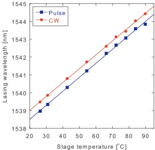
Next, we measured the lasing wavelength as a func- tion of the stage temperature under pulse and CW pumping conditions. The result is shown in Fig. 7. The sample tem- perature was well controlled by the stage temperature since the lasing wavelengths were proportional to the stage tem- peratures. The proportional constant was 0.079 nm/K. We found that CW pumping raised the active region tempera- ture by 7.4
◦C. The value agreed with the calculated results we reported in [5], which were numerical calculations of the temperature distribution in the PhC laser. The PhC laser temperature increase was calculated to be 6.7
◦C with a 100- µW heat source in the simulation.
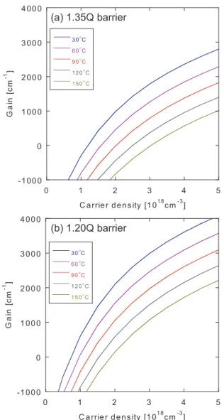
Since the output power of the PhC laser is not large enough to be used for practical optical interconnections, we carried out simulations to discuss further improvement of the temperature characteristics. The gain was calculated as a function of carrier density using a combination of the 6- band k · p method and Fermi’s golden rule [17]. The results are shown in Fig. 8. When the temperature increases, the gain decreases and it is di ffi cult to have threshold gain for a multiple quantum well (MQW) with 1.35Q barriers above 90
◦C. In contrast, when we use 1.20Q barriers, the gain is larger than with 1.35Q barriers, and it will be possible to ob- tain lasing above 150
◦C owing to the larger conduction band offset. The temperature characteristics we have presented will be greatly improved by employing an MQW with 1.20Q barrier layers.
3.3 Frequency Response
Finally we measured the small-signal response of the PhC
laser at RT and 66.2
◦C. The measurement setup is shown in
Fig. 9. To measure the responses, we modulated the 1.31-
µm pump light with a lithium-niobate (LN) modulator using
Fig. 6 LL characteristic of the PhC laser for various stage temperatures on (a) linear and (b) logarithmic scales. The device could be operated at 89.8◦C with CW pumping. The lattice constant of this device was 436 nm.
a network analyzer. The pump light was filtered from the output light using a 1.3/1.55-µm WDM filter. The lasing light was amplified through an erbium doped fiber ampli- fier (EDFA) and detected with a network analyzer. We sub- tracted the frequency response of the LN modulator from the measured data, which contained the responses both from the modulator and the device, to extract the responses of the PhC laser.
The results at RT and 66.2
◦C are shown in Figs. 10(a) and (b), respectively. The pump-light power was changed from −19.7 to −7.8 dBm in Fig. 10(a), and −15.9 to
Fig. 7 Lasing wavelengths as a function of stage temperatures. Blue- square and red-circle plots correspond to the pulse and CW pumping con- ditions, respectively. We found that the lasing wavelengths were propor- tional to the stage temperature with a proportional constant of 0.079 nm/K.
The pump power was 117µW at the waveguide. The stage temperature was correctly transferred to the sample. The CW pumping raised the sam- ple temperature by 7.4◦C, which could be determined from the difference between the two curves.
−8.1 dBm in Fig. 10(b). We could acquire the frequency responses of the PhC lasers using the abovementioned method. Clear resonant frequencies were observed at both RT and 66.2
◦C. We obtained maximum 3-dB bandwidths of 11.6 and 7.0 GHz at RT and 66.2
◦C, respectively. The dy- namic characteristics at 66.2
◦C were limited due to the re- duction in the di ff erential gain and the increase in the thresh- old power. A 1.20Q barrier, which increases the band offset, in an MQW is the effective way not only to improve temper- ature characteristics but also to increase output power.
3.4 Discussion of Interconnection Bandwidth
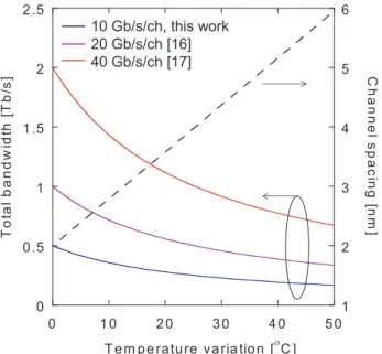
WDM is essential for on-chip optical interconnection if we are to meet the demand for a 1-Tb/s total bandwidth [3].
Using the lasing wavelength accuracy (Fig. 4), temperature- dependent lasing wavelength (Fig. 7), and small-signal re- sponse (Fig. 10) data we have presented, we can estimate the channel spacing of the WDM signal and the total band- width of the interconnection.
Figure 11 plots the wavelength variation and total
bandwidth of the interconnection versus the temperature
variation of the chip. We calculated the channel spacing
as the sum of the ±1-nm fabrication error and the wave-
length shift caused by the temperature variation. The result
is shown as a dashed line in Fig. 11. When the chip tem-
perature is stable, it is possible to arrange 50 channels in a
100-nm bandwidth with a 2-nm channel spacing. Since 10-
Gb/s modulation will be available with the 3-dB bandwidth
we presented, a total bandwidth of 500 Gb/s can be achieved
as shown by the blue solid line in Fig. 11. When we assume
Fig. 8 Calculated gain of the MQWs with (a) a 1.35Q barrier (current design) and (b) a 1.20Q barrier. An MQW with a 1.20Q barrier has a higher gain than one with a 1.35Q barrier.
Fig. 9 The measurement setup for the frequency responses of the PhC lasers. We modulated the pump light using an LN modulator. The fre- quency response of the LN modulator was subtracted from the measured data to extract the PhC characteristics.
that the modulation speed of each channel is 20 Gb / s, which has already been demonstrated at RT [18], it is possible to achieve a total bandwidth of 1 Tb / s. On the other hand, the total bandwidth is limited to 314 Gb/s if there is a 15
◦C tem- perature variation [3] on the CMOS chip. To enhance the modulation bandwidth of PhC lasers, we have developed in- jection locking and already obtained 40 Gb/s direct modu-
Fig. 10 Small signal responses of the PhC laser at (a) RT and (b) 66.2◦C.
We measured the responses by modulating the pump light using an LN modulator. The maximum 3-dB bandwidths were 11.6 and 7.0 GHz at RT and 66.2◦C, respectively.
lation and a frequency response of over 67 GHz [19], [20].
By using this technique, we can fabricate an optical inter- connection in which each channel has a 40-Gb/s bandwidth.
The red solid line in Fig. 11 shows the total bandwidth ver- sus the temperature variation with a 40-Gb/s bandwidth in each channel. A total bandwidth of 1 Tb/s can be obtained as long as the temperature variation is less than 25
◦C. A 1- Tb / s bandwidth at 25
◦C meets the requirement and makes PhC lasers promising devices as on-chip light sources.
4. Conclusion
This paper described high-temperature CW operation of a
PhC laser up to 89.8
◦C as well as a wide wavelength range
of 100 nm at RT. The wavelength errors as regards hole di-
ameter and active region width were suppressed to ± 0.22
and 13 nm, respectively. Furthermore, we measured the dy-
namic responses of the PhC laser at RT and 66.2
◦C with
maximum 3-dB bandwidths of 11.6 and 7.0 GHz, respec-
tively. These wide temperature and wavelength operat-
Fig. 11 Calculated channel spacing (dashed line) and total bandwidth of the interconnection (solid line) as a function of temperature variation.
10, 20, and 40 Gb/s operation speeds are assumed at each channel in the blue, purple, and red solid line, respectively. We will be able to achieve a total bandwidth of more than 1 Tb/s by means of injection locking, since injection locking increases the modulation bandwidth to over 40 Gb/s.
ing ranges make PhC lasers promising candidates as light sources for on-chip optical interconnections, and a total bandwidth of 1 Tb/s will be possible for future on-chip opti- cal interconnection using PhC lasers.
Acknowledgment
Part of this work was supported by the National Institute of Information and Communications Technology (NICT).
References
[1] N. Magen, A. Kolodny, U. Weiser, and N. Shamir, “Interconnect- power dissipation in a microprocessor,” System Level Interconnect Prediction (SLIP), 2004.
[2] M. Haurylau, G. Chen, H. Chen, J. Zhang, N.A. Nelson, D.H.
Albonesi, E.G. Friedman, and P.M. Fauchet, “On-chip optical inter- connect roadmap: Challenges and critical directions,” IEEE J. Sel.
Top. Quantum Electron., vol.12, no.6, pp.1699–1705, 2006.
[3] Y. Vlasov, “Silicon photonics for next generation computing sys- tems,” Europ. Conf. Opt. Commun., paper Tu.1.A.1., 2008.
[4] D.A.B. Miller, “Device requirements for optical interconnects to sil- icon chips,” Proc. IEEE, vol.97, no.7, pp.1166–1185, July 2009.
[5] S. Matsuo, A. Shinya, T. Kakitsuka, K. Nozaki, T. Segawa, T. Sato, Y. Kawaguchi, and M. Notomi, “High-speed ultracompact buried heterostructures photonic-crystal laser with 13 fJ of energy con- sumed per bit transmitted,” Nature Photonics, vol.4, no.9, pp.648–
654, Sept. 2010.
[6] B. Ellis, M.A. Mayer, G. Shambat, T. Sarmiento, J. Harris, E.E.
Haller, and J. Vuˇckovi´c, “Ultralow-threshold electrically pumped quantum-dot photonic-crystal nanocavity laser,” Nature Photonics, vol.5, pp.297–300, 2011.
[7] C.M. Long, A.V. Giannopoulos, and K.D. Choquette, “Lateral cur- rent injection photonic crystal membrane light emitting diodes,” J.
Vacuum Science & Technology B, vol.28, no.2, pp.359–364, 2010.
[8] K. Tanabe, M. Nomura, D. Guimard, S. Iwamoto, and Y. Arakawa,
“Room temperature continuous wave operation of InAs/GaAs quan- tum dot photonic crystal nanocavity laser on silicon substrate,” Opt.
Express, vol.17, no.9, pp.7036–7042, 2009.
[9] L.J. Mart´ınez, B. Al´en, I. Prieto, D. Fuster, L. Gonz´alez, Y.
Gonz´alez, M.L. Dotor, and P.A. Postigo, “Room temperature con- tinuous wave operation in a photonic crystal microcavity laser with a single layer of InAs/InP self-assembled quantum wires,” Opt. Ex- press, vol.17, no.17, pp.14993–15000, 2009.
[10] S. Imai, K. Takaki, S. Kamiya, H. Shimizu, J. Yoshida, Y. Kawakita, T. Takagi, K. Hiraiwa, H. Shimizu, T. Suzuki, N. Iwai, T. Ishikawa, N. Tsukiji, and A. Kasukawa, “Recorded low power dissipation in highly reliable 1060-nm VCSELs for green optical interconnection,”
IEEE J. Sel. Top. Quantum Electron., vol.17, no.6, pp.1614–1620, 2011.
[11] M. M¨uller, W. Hofmann, T. Gr¨undl, M. Horn, P. Wolf, R.D. Nagel, E. R¨onneberg, G. B¨ohm, D. Bimberg, and M.-C. Amann, “1550- nm High-Speed Short-Cavity VCSELs,” IEEE J. Sel. Top. Quantum Electron., vol.17, no.5, pp.1158–1166, 2011.
[12] M.P. Nezhad, A. Simic, O. Bondarenko, B. Slutsky, A. Mizrahi, L.
Feng, V. Lomakin, and Y. Fainman, Room-temperature subwave- length metallo-dielectric lasers, Nature Photonics, vol.4, pp.395–
399, 2010.
[13] M.T. Hill, Y.-S. Oei, B. Smalbrugge, Y. Zhu, T. de Vries, P.J. van Veldhoven, F.W.M. van Otten, T.J. Eijkemans, J.P. Turkiewicz, H.
de Waardt, E.J. Geluk, S.-H. Kwon, Y.-H. Lee, R. N¨otzel, and M.K.
Smit, “Lasing in metallic-coated nanocavities,” Nature Photonics, vol.1, pp.589–594, 2007.
[14] W.-D. Ho, T.-W. Lu, Y.-H. Hsiao, and P.-T. Lee, “Thermal prop- erties of 12-fold quasi-photonic crystal microcavity laser with size- controlled nano-post for electrical driving,” J. Lightwave Technol., vol.27, no.23, pp.5302–5307, 2009.
[15] S. Matsuo, A. Shinya, T. Kakitsuka, K. Nozaki, T. Segawa, T. Sato, Y. Kawaguchi, and M. Notomi, “Ultra-small InGaAsP/InP buried heterostructure photonic crystal laser,” IEEE Photonic Society An- nual Meeting, paper WH3, 2009.
[16] S. Nishihara, S. Kimura, T. Yoshida, M. Nakamura, J. Terada, K.
Nishimura, K. Kishine, K. Kato, Y. Ohtomo, N. Yoshimoto, T.
Imai, and M. Tsubokawa, “A burst-mode 3R receiver for 10-Gbit/s PON systems with high sensitivity, wide dynamic range, and fast response,” J. Lightwave Technol., vol.26, no.1, pp.99–107, 2008.
[17] S.L. Chuang, Physics of Optoelectronic Devices, John Willey &
Sons, New York, 1995.
[18] S. Matsuo, A. Shinya, C.-H. Chen, K. Nozaki, T. Sato, Y.
Kawaguchi, and M. Notomi, “20-Gbit/s directly modulated buried heterostructure photonic crystal laser with 8.76-fj/bit operating en- ergy,” Europ. Conf. Opt. Commun., paper PD1.6, 2010.
[19] C.-H. Chen, K. Takeda, A. Shinya, K. Nozaki, T. Sato, Y.
Kawaguchi, M. Notomi, and S. Matsuo, “40-Gb/s directly- modulated photonic crystal lasers under optical injection-locking,”
Opt. Express, vol.19, no.8, pp.17669–17676, 2011.
[20] C.-H. Chen, K. Takeda, A. Shinya, K. Nozaki, T. Sato, M. Notomi, K. Kato, and S. Matsuo, “Optically Injection-locked photonic crystal laser with>67 GHz modulation bandwidth,” Electron. Lett., vol.47, no.22, pp.1240–1241, 2011.
cal interconnect, InP photonic integrated cir- cuit, and photonic crystal lasers. Dr. Takeda is a member of the IEEE Photonics Society and Japan Society of Applied Physics (JSAP). He re- ceived the Best Student Paper Award from IEEE Photonics Society in 2009, and the Outstanding Presentation Award from JSAP in 2010.
Tomonari Sato was born in Gunma, Japan, in 1978. He received the B.E., M.E., and Ph.D. degrees in engineering from University of Tsukuba, Ibaraki, Japan, in 2001, 2003, and 2009, respectively. In 2003, he joined NTT Pho- tonics Laboratories, Nippon Telegraph and Tele- phone Corporation (NTT), Kanagawa, Japan.
He has been engaged in research on the MOVPE growth of III-V semiconductors and develop- ment of semiconductor lasers for sensor applica- tions. Dr. Sato is a member of the Japan Society of Applied Physics.
Takaaki Kakitsuka was born in Kuma- moto, Japan, in 1971. He received the B.S. and M.S. degrees in physics in 1994 and 1996, and Dr. Eng. degree in 2012 from Kyushu Univer- sity, Fukuoka, Japan. In 1996, he joined NTT Opto-electronics Laboratories, Nippon Tele- graph and Telephone Corporation (NTT), Kana- gawa, Japan. He has been engaged in research on semiconductor lasers and optical functional devices. From 2009 to 2011, he was a mem- ber of research and development planning de- partment. He is now with NTT Photonics Laboratories. Dr. Kakitsuka is a member of IEEE, Japan Society of Applied Physics, and Physical Society of Japan.
Akihiko Shinya received the B.E., M.E., and Dr. Eng. degrees in electrical engineering from Tokushima University in 1994, 1996, and 1999, respectively. He joined NTT Basic Re- search laboratories in 1999 and has been en- gaged in R&D of photonic crystal nanodevices.
Dr. Shinya is a member of the Japan Society of Applied Physics.
switches, memories, and electro-optic devices based on photonic crystals and related photonic nanostructures. Dr. Nozaki is a member of the Japan Society of Applied Physics (JSAP).
Chin-Hui Chen received the B.S. degree in electrical engineering from the National Tai- wan University, Taipei, Taiwan, in 2002 and the M.S. and Ph.D. degrees in electrical and com- puter engineering from the University of Cal- ifornia, Santa Barbara, in 2004 and 2009, re- spectively. From 2002 to 2009, she was a Re- search Assistant with the Optoelectronics Tech- nology Center, University of California, Santa Barbara. Since 2009, she has been a Postdoc- toral Research Associate with NTT Photonics Laboratories. Her current research interests include ultralow-power optical interconnect, optical injection-locking, high-speed modulation, nanopho- tonic devices, and InP photonic integrated circuits. Dr. Chen is a mem- ber of IEEE and the Photonics Society. She received the Taiwan National Science Council Undergraduate Project Award in 2002, the Outstanding Student Presentation Award from Asia Optical Fiber Communication and Optoelectronic Exposition and Conference in 2008, and the Best Presenta- tion Award from Japan Technical Group of Laser and Quantum Electronics in 2010.
Hideaki Taniyama received the B.S. and M.S. degrees from Osaka Prefectural Univer- sity, Osaka, Japan, in 1986 and 1988, respec- tively, and the Ph.D. degree from Osaka Uni- versity, Osaka, Japan, in 1996. He joined NTT LSI Laboratories, Atsugi, Kanagawa, Japan, in 1988, where he was engaged in the research of device physics and modeling, including quan- tum effects. In 1998, he joined ATR Adaptive Communications Research Laboratories, Kyoto, Japan. During 1999, he was a Visiting Re- searcher with Arizona State University, Tempe. From 2001 to 2003, he was a member of the NTT Photonics Laboratories. In 2003, he joined the NTT Basic Research Laboratories, where he has since been engaged in the research of photonic nanostructures. Dr. Taniyama is a member of the American Physical Society, the Physical Society of Japan, and the Japan Society of Applied Physics.
Masaya Notomi received B.E., M.E. and Ph.D. degrees in applied physics from Univer- sity of Tokyo, Japan in 1986, 1988, and 1997, respectively. In 1988, he joined NTT. Since then, his research interest has been to control the optical properties of materials/devices by ar- tificial nanostructures (quantum wires/dots and photonic crystals). He is a group leader of Pho- tonic Nanostructure Research Group and Senior Distinguished Scientist in NTT Basic Research Laboratories. He is also a guest professor of To- kyo Institute of Technology. He received IEEE/LEOS Distinguished Lec- turer Award (2006), JSPS prize (2009), Japan Academy Medal (2009), and The Commendation by Japanese Minister of Education (2010). He is serv- ing as a member of National University Corporation Evaluation Committee in the Japanese government. Dr. Notomi is a member of the Japan Society of Applied Physics, American Physical Society (APS), IEEE, and Optical Society of America (OSA).
Shinji Matsuo received the B.E. and M.E.
degrees in electrical engineering from Hiro- shima University, Hiroshima, Japan, in 1986 and 1988, and the Ph.D. degree in electronics and applied physics from Tokyo Institute of Tech- nology, Tokyo, Japan, in 2008. In 1988, he joined NTT Opto-electronics Laboratories, At- sugi, where he was engaged in research on pho- tonic functional devices using MQW-pin modu- lators and VCSELs. In 1997, he researched op- tical networks using WDM technologies at NTT Network Innovation Laboratories, Yokosuka. Since 2000, he has been re- searching high-speed tunable optical filters and lasers for photonic packet switching at NTT Photonics Laboratories, Atsugi. Dr. Matsuo is a member of the IEEE Photonics Society, Japan Society of Applied Physics.