Japan Advanced Institute of Science and Technology
JAIST Repository
https://dspace.jaist.ac.jp/
Title
Electrical properties of nearly stoichiometric
GaAs grown by molecular beam epitaxy at low
temperature
Author(s)
Fukushima, S.; Obata, T.; Otsuka, N.
Citation
Journal of Applied Physics, 89(1): 380-385
Issue Date
2001-01-01
Type
Journal Article
Text version
publisher
URL
http://hdl.handle.net/10119/4538
Rights
Copyright 2001 American Institute of Physics.
This article may be downloaded for personal use
only. Any other use requires prior permission of
the author and the American Institute of Physics.
The following article appeared in S. Fukushima,
T. Obata, and N. Otsuka, Journal of Applied
Physics, 89(1), 380-385 (2001) and may be found
at http://link.aip.org/link/?JAPIAU/89/380/1
Description
Electrical properties of nearly stoichiometric GaAs grown by molecular
beam epitaxy at low temperature
S. Fukushima, T. Obata, and N. Otsukaa)
School of Materials Science, Japan Advanced Institute of Science and Technology, Asahidai 1-1, Tatsunokuchi, Nomigun, Ishikawa 923-1292, Japan
共Received 5 June 2000; accepted for publication 9 October 2000兲
Nearly stoichiometeric GaAs epilayers doped with Si or Be were grown by molecular beam epitaxy at a low temperature with closely controlled fluxes near the stoichiometric conditions. Excess As point defects in the epilayers which acted as trap sites of free carriers were studied by means of the Hall effect measurements. Under the same As/Ga flux condition, concentrations of excess As point defects which trap free carriers increase with increase of concentrations of Si or Be. With the same concentration of the dopants, on the other hand, concentrations of excess As point defects increase linearly with the As/Ga flux ratio. The dependence of carrier mobility on the trapped carrier concentrations indicates that free carriers are trapped by neutral point defects and change them into ionized ones. In the epilayers which are very close to the stoichiometric composition, Si exhibits its amphoteric nature, occupying both donor and acceptor sites and results in the self-compensation. © 2001 American Institute of Physics. 关DOI: 10.1063/1.1330765兴
I. INTRODUCTION
GaAs epilayers grown at low temperatures 共LT-GaAs兲 exhibit a number of novel properties such as high electrical resistivity and ultra-fast response to photoexcitation.1,2These properties result from high concentrations of excess As in the epilayers. Among these properties, ultra-fast response to photoexcitation, that is, ultra-short lifetime of photoexcited carriers, is attracting a great deal of attention. In recent years LT-GaAs has been extensively studied, aimed at applications to optoelectronic devices such as THz electromagnetic pulse generators3–5 and also all-optical switches6–8 which will have a large impact on the future optoelectronic technology. Studies on excess As point defects in LT-GaAs have been carried out so far mainly by means of spectroscopic techniques and theoretical calculations. The main excess As point defects are antisite As, AsGa, and their concentrations
have been measured by means of the near infrared absorption spectroscopy.9,10 Because of the linear correlation between the concentration of AsGaand lattice expansion of LT-GaAs epilayers, almost all excess As are considered to be AsGa.10 According to the theoretical study,11AsGais known to act as a double donor. Nearly one order of magnitude smaller con-centrations of AsGa were found to be singularly ionized in undoped LT-GaAs by means of the electron spin resonance spectroscopy.12 In addition to AsGa, the slow positron
anni-hilation has shown the existence of Ga vacancies, VGa, in
this material.13 The theoretical study indicates that VGais a
triple acceptor.14 Besides these point defects, existence of defect complexes and interstitial As atoms has been suggested,15,16 but their existence has not been experimen-tally confirmed without ambiguity. Even if they are present, their concentrations are considered to be much smaller than
that of AsGa. A recent study has shown that the
concentra-tion of singularly ionized AsGa is three times the
concentra-tion of VGa in undoped LT-GaAs, implying that these point
defects compensate each other.17
Relaxation processes of photoexcited carriers in LT-GaAs have been studied by means of the pump-probe method.18–25According to these studies, photoexcited carri-ers are first trapped by excess As point defects in subpico-seconds and recombine in relatively long times in as-grown LT-GaAs. It is suggested that photoexcited electrons are trapped by positively ionized AsGaand holes are trapped by
negatively ionized VGa. In annealed LT-GaAs, on the other
hand, metallic clusters of excess As act as recombination centers of photoexcited carriers.19
In order to have improvement of the properties of LT-GaAs as THz electromagnetic pulse generators and to realize all-optical switches based on LT-GaAs, it is necessary to have further understanding of excess As point defects, which will enable one to develop new methods for control of their concentrations and spatial distribution. In the study reported in this article, we have investigated excess As point defects by utilizing a method different from those employed up to the present for the studies of LT-GaAs. Nearly stoichio-metric LT-GaAs epilayers were grown with donor or accep-tor dopants, and the dependence of their electrical properties on the concentration of excess As point defects were studied by Hall effect measurements. From this study, new insights of excess As point defects which trap charge carriers have been obtained. The results also clarify new fundamental as-pects of low temperature molecular beam epitaxy 共MBE兲 growth of compound semiconductors.
In earlier studies, O’Hagan et al., have showed that the concentration of excess As in LT-GaAs can be considerably reduced by lowering the As flux with respect the Ga flux and the conduction by free carriers was observed in the doped epilayers grown under such flux conditions.26In recent
stud-a兲Author to whom correspondence should be addressed; electronic mail:
ootsuka@jaist.ac.jp
380
ies, Suda and Otsuka have investigated the dependence of the concentration of excess As on the As/Ga flux ratio for different growth temperatures and made the following two findings.27,28The first finding is that one can obtain stoichio-metric LT-GaAs epilayers regardless of the growth tempera-ture under the flux condition where the As/Ga flux ratio cor-responds to the number ratio of As4 molecules and Ga atoms
in the dissociation reaction proposed by Foxon and Joyce.29 The other is that the dependence of the concentration of ex-cess As on the As/Ga flux ratio at a fixed growth temperature is described in terms of the Langmuir adsorption isotherm and, hence, the concentration can be closely controlled by the flux condition. In the present study, based on these re-sults, the concentration of excess As was systematically var-ied in the vicinity of the stoichiometric composition, and the concentration and mobility of free carriers were measured as a function of the concentration of excess As.
II. EXPERIMENT A. MBE growth
LT-GaAs epilayers were grown by utilizing a conven-tional molecular beam epitaxy 共MBE兲 system. The back-ground pressure of the growth chamber was less than 5 ⫻10⫺10Torr, and semi-insulating epi-ready共100兲GaAs wa-fers were used as substrates. For each growth experiment, a substrate which was cut into a size of 18⫻15 mm2 was mounted on a Mo holder with indium. After desorption of a oxide layer of the substrate surface, the surface was annealed with the As flux for 10 min at 600 °C, followed by the growth of a GaAs buffer layer of a thickness of 150 nm at 580 °C. After the growth of the buffer layer, the temperature of the sample was lowered to 270 °C at which all LT-GaAs epilayers were grown in this study.
The temperature of the sample surface was measured by using a quartz rod connected to a pyrometer before and after the growth of each LT-GaAs epilayer. Details of the method of this temperature measurement was described in an earlier report.27 The reason for the choice of 270 °C as the growth temperature of LT-GaAs epilayers is that the dependence of the concentration of excess As on the As/Ga flux ratio at this temperature is given as the simplest form of the Langmuir adsorption isotherm:
关Asex兴⫽JAs/JGa⫺1 JAs/JGa 关As
ex兴
sat, 共1兲
where关Asex兴 and 关Asex]
satare the concentration of excess As
for the As flux JAs and Ga flux JGa and the saturated con-centration of excess As at the growth temperature 270 °C, respectively.28 In order to obtain a stable As flux during the growth, the As effusion cell was maintained at a given tem-perature up to 2 h prior to the growth. All LT-GaAs epilayers were grown for 40 min, and the Ga flux was maintained at a constant ion gauge reading, (5.2⫾0.1)⫻10⫺7 Torr, which gives rise to a thickness of the epilayers, 600 nm. The As flux was varied for LT-GaAs epilayer grown in this study in the range of ion gauge readings between 6.5⫻10⫺6 and 1.1 ⫻10⫺5Torr. The readings of As fluxes after the growth did not change from those before the growth by more than 2%.
Si was doped as a donor dopant with concentrations of either 1.58⫻1018 or 3.40⫻1018 cm⫺3, and Be was doped as an acceptor dopant with concentrations of either 5.44⫻1018 or 9.44⫻1018 cm⫺3. The concentrations of the dopants were calibrated by measuring carrier concentrations in doped GaAs epilayers grown at 580 °C where nearly all dopants provide free carriers at room temperature.
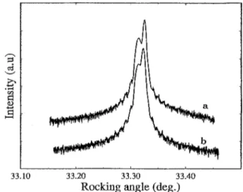
In all growth experiments, the substrate holder was not rotated during the growth, and substrates were positioned in such a way that a slight change in the flux ratio was inten-tionally introduced along the longer edge of a substrate. In this way a number of data points of the dependence of the electrical property on the concentration of excess As were obtained from one sample. Figure 1 are x-ray 400 rocking curves measured from two points 共a兲 and 共b兲 of a low Be-doped epilayer which was grown with a Ga flux, 5.2 ⫻10⫺7 Torr, and As flux, 8.2⫻10⫺6 Torr. The two points were apart from each other by 6 mm along the longer edge. From these rocking curves, the changes of lattice spacings of LT-GaAs epilayers,␦d/d, were determined, and then corre-sponding flux ratios at two points were estimated by using the equation derived by Suda and Otsuka,28
冉
␦d d冊
⫽ JAs/JGa⫺1 JAs/JGa冉
␦d d冊
sat, 共2兲where (␦d/d)sat is the saturation value at 270 °C, being 0.705⫻10⫺3. The flux ratios derived from the two points共a兲 and共b兲 are 1.644 and 1.520, respectively, which gives rise to a gradient of the flux ratio along the sample surface of 0.0206/mm with the assumption of a linear change of the flux ratio. From the epilayer which was grown with a higher As flux, a similar value of the change of the flux ratio was obtained. The change of the flux ratio over the epilayer sur-face seems to have resulted mainly from a nonuniformity of the As flux because the thickness of the epilayer was nearly constant over the epilayer according to the fringe spacings in the x-ray rocking curves.
FIG. 1. X-ray diffraction rocking curves of 400 reflections taken from two points of a LT-GaAs epilayer. Two points are apart from each other by 6 mm in the direction of the change of the flux ratio with the one共a兲 being on the higher flux ratio side and the other共b兲 on the lower flux side.
381
For epilayers which are closer to the stoichiometric com-position, ␦d/d cannot be accurately measured from x-ray rocking curves, and, hence, a flux ratio at each point of the epilayers was estimated in the following method. The ion gauge reading is considered to represent the average As flux over the epilayer surface, and, therefore, it is considered to correspond to the As flux at the center of the surface. By comparing an ion gauge reading of an epilayer with the ion gauge reading of the reference epilayer whose x-ray rocking curves are shown in Fig. 1, the flux ratio at the center of the former epilayer was determined. Next, flux ratios at other points of the epilayer surface were estimated by using the above-mentioned gradient of the flux ratio, that is, 0.0206/ mm. For the epilayers grown in this study, the flux ratio JAs/JGaranges from 0.92 to 1.70. In the case that a flux ratio
becomes less than 1.0, the surface always appear nonmirror-like, indicating that the above-mentioned method for assign-ing the flux ratio to a given point of an epilayer surface is a reasonable one. In order to examine the accuracy of the above-mentioned method of determination of a flux ratio at each point of an epilayer surface, two epilayers were grown by rotating the substrate holder during the growth. The ion gauge readings of As fluxes of the two epilayers were 5.9 ⫻10⫺6 and 7.6⫻10⫺6 Torr, corresponding to flux ratios 0.967 and 1.338, respectively. The x-ray rocking curves tained from these rotated epilayers closely match those ob-tained from two points of the unrotated epilayer whose flux ratios are considered to be the same as the above two values according to the assumption of the linear change of the As flux along the epilayer surface. The surface of the rotated epilayer grown with the flux ratio 0.967 was also found to be nonmirrorlike as in the case of unrotated epilayers.
B. Hall effect measurement
All epilayers grown in the study were examined by the Hall effect measurements with the van der Pouw method. The samples for the measurements were made in the follow-ing way. From all epilayers, a set of three square pieces with a size of 5⫻5 mm2were cut in the direction of the increase of the flux ratio. For the epilayers which are very close to the stoichiometric composition, a set of smaller pieces with a size of 2⫻2 mm2were obtained from the region of the non-mirrorlike surface to that of the non-mirrorlike surface. Indium contacts were made at corners of each piece, and the piece was annealed at 270 °C from 10 to 30 min in a nitrogen atmosphere in order to obtain ohmic contacts. The Hall ef-fect measurements were made at room temperature.
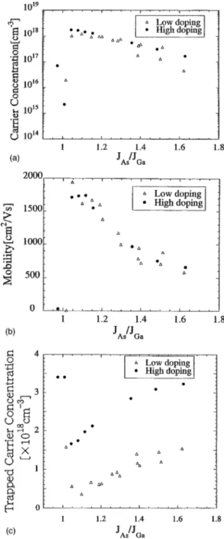
Figures 2共a兲–2共c兲 are the results of Si-doped epilayers. Figure 2共a兲 shows the dependence of the charge carrier con-centration on the flux ratio. For both high doping and low doping, the carrier concentration monotonously increases as the flux ratio decreases towards 1.0. The carrier concentra-tion, however, reaches maxima around the flux ratio 1.04 and sharply decreases at lower flux ratios. This sharp decrease of the carrier concentration starts at the location where the sur-face is still mirrorlike. The conduction type in this low car-rier concentration region is the p type, unlike other regions which exhibit the n type conduction. Figure 2共b兲 is the
de-pendence of the mobility on the flux ratio. For both doping conditions, the mobility increases with the decrease of the flux ratio except for the range from nearly 1.0 to the lower ratio. By comparing this dependence with that of Fig. 2共a兲, one can find that the mobility increases with the increase of the carrier concentration in the present case.
Figure 2共c兲 shows the trapped carrier concentration as a function of the flux ratio. The trapped carrier concentration is derived by subtracting the free carrier concentration from the dopant concentration. For both high doping and low doping, the figure shows a nearly linear increase of the trapped
car-FIG. 2. Results of Hall effect measurements of samples cut from Si-doped LT-GaAs epilayers which were grown under different flux ratios:共a兲 charge carrier concentrations,共b兲 mobility, and 共c兲 trapped carrier concentrations.
rier concentration from the stoichiometric value to 1.6, be-yond which the concentration remains nearly constant at the values of the dopant concentrations. Besides the linear in-crease of the trapped carrier concentration, the figure shows another important point. In the range where the concentration linearly increases, values of trapped carrier concentrations of high doping and low doping are significantly different from each other at the same flux ratio; the trapped carrier concen-tration of high doping is much greater than that of low dop-ing at a given flux ratio.
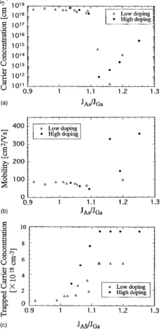
Figures 3共a兲–3共c兲 are the results of Be-doped epilayers. The carrier concentration, mobility and trapped carrier con-centration exhibit similar trends to those of Si-doped epilay-ers in the region of the flux ratio less than 1.1 where carrier concentrations are on the order of 1018 cm⫺3. These trends are monotonous increase of the carrier concentration towards the unity flux ratio, the increase of the mobility with the
increase of the carrier concentration, the linear increase of the trapped carrier concentration with the increase of the flux ratio from the unity flux ratio, and different trapped carrier concentrations at a given flux ratio for high doping and low doping. There is, however, one difference from the case of the Si-doped epilayers. In this case the carrier concentration remains high even for the flux ratio below 1.0, and the con-duction type remains as the p type throughout this range including the region where the surface is nonmirrorlike. There is another interesting point for the Be-doped epilayers. In the higher flux ratio range where the trapped carrier con-centrations saturate, the conduction type has changed into the n type, and the carrier concentration gradually increases with the increase of the flux ratio, especially in the case of high doping.
III. DISCUSSION
As mentioned in the Introduction, among a number of excess As point defects, existence of AsGaand VGahave been
experimentally confirmed to date without ambiguity. In this article, therefore, the results of the study are discussed by referring to these two types of point defects. Antisite As, AsGa, is known to act as a deep donor, and VGa as a deep acceptor. Hence, the former is expected to trap a hole pro-vided by Be, and the latter is expected to trap an electron given by Si. The results presented in the previous section are reasonably explained with this picture. It has been shown that the majority of excess As point defects are considered to be AsGa, while the concentration of VGa, on the other hand,
is known to be one order of magnitude smaller than that of AsGa.17As seen in Figs. 2共c兲 and 3共c兲, trapped carrier
con-centrations in the Be-doped epilayers are nearly one order of magnitude greater than those in the Si-doped epilayers, indi-cating that holes are trapped by AsGaand electrons by VGa.
The correlation of the mobility with the carrier concen-tration is also explained with this picture. The mobility of charge carriers in both Si-doped epilayers and Be-doped epi-layers decrease with increasing trapped carrier concentra-tions in the region where free carriers are present. This im-plies that trapping of charge carriers results in ionizations of point defects and, hence, leads to larger scattering of charge carriers. Therefore, one can interpret the present results in such a way that holes are trapped by neutral AsGa, resulting
in positively ionized point defects, and electrons are trapped by neutral VGa, resulting in negatively ionized point defects. There is another result which fits well to this picture. In the Be-doped epilayers, the conduction type becomes the n type in the flux range where the trapped carrier concentration saturates, all free carriers being trapped, and charge carrier concentrations increase with the further increase of the As flux. In this range, nearly all AsGaare positively ionized with
a few remaining as neutral AsGa. Electrons of neutral AsGa,
hence, can move to ionized AsGa, resulting in the hopping
conduction of electrons. With further increase of the As flux, the concentration of neutral AsGaincreases and results in the
increase of the concentration of hopping electrons.
The linear increase of trapped carrier concentrations with the increase of the flux ratio from unity in both
Si-FIG. 3. Results of Hall effect measurements of samples cut from Be-doped LT-GaAs epilayers which were grown under different flux ratios:共a兲 charge carrier concentrations,共b兲 mobility, and 共c兲 trapped carrier concentrations.
383
doped and Be-doped epilayers is explained in terms of the Langmuir adsorption model proposed by Suda and Otsuka.28 According to Eq.共1兲, the concentration of excess As linearly increases with the increase of the flux ratio from unity in the vicinity of the stoichiometric flux condition. The present re-sults indicate that concentrations of both AsGa and VGa
change with the flux ratio according to this Langmuir adsorp-tion model. The results also indicate that concentraadsorp-tions of these excess As point defects approach to approximately zero as the flux ratio moves to unity, except for a sudden increase around the stoichiometric flux condition in the case of Si-doped epilayers. Because of the intentional change of the flux ratio over an epilayer surface and a slight change of the As flux during the growth of a LT-GaAs epilayer, we did not obtain a LT-GaAs epilayer where no significant concentra-tion of trapped carriers exists and, hence, a free carrier con-centration is exactly equal to the dopant concon-centration. The present results, however, suggest that one could obtain a LT-GaAs epilayer close to such a condition if the fluxes were carefully controlled for the growth.
Figures 2共c兲 and 3共c兲 show that trapped carrier trations have increased with the increase of dopant concen-trations for a given flux ratio. This means that more VGaare
incorporated with a higher Si concentration and more AsGa
with a higher Be concentration. Such a tendency has never been observed in earlier studies of LT-GaAs. A higher dop-ant concentration is obtained with a higher effusion cell tem-perature, which will result in a slightly higher epilayer sur-face temperature during the growth due to the thermal irradiation. The above-mentioned tendency of the incorpora-tion of excess As point defects is opposite to that expected from this thermal effect. A more reasonable cause of the present results is the tendency of reducing free carrier con-centrations in a semiconductor material, since the presence of a high concentration of free carriers implies that the elec-tronic system of a semiconductor is in a higher energy state than that of an intrinsic semiconductor. In other words, an electronic system of a semiconductor has an intrinsic ten-dency to try to keep the Fermi level at the midgap. When a higher concentration of Si is doped, more VGa, which are
deep acceptors, are incorporated for a given flux condition. Similarly, more AsGa, which are deep donors, are
incorpo-rated when a higher concentration of Be is doped. It is inter-esting to note that such an intrinsic tendency of the electronic system of a semiconductor occurs even in the case of the low temperature growth of MBE where only surface atoms are movable via surface migration and desorption.
In earlier studies,30 it was found that incorporation of a high concentration of dopants leads to significant reduction of the concentration of excess As even under the high As flux condition. The doping concentrations employed in these studies were on the order of 1019 cm⫺3, which are much higher than those employed in the present study. This effect of the dopant on the incorporation of excess As is opposite to the present case. We believe that the reduction of the con-centration of excess As by the high concon-centration of dopants is explained in the following way. According to the Lang-muir adsorption model for incorporation of excess As in LT-GaAs,28chemisorbed As atoms on the As terminated
sur-face of GaAs serve as a precursor of excess As atoms. Ar-rival of a high concentration of dopant atoms on such a sur-face is likely to disturb chemisorbed As atom layers and, hence, reduce the incorporation of excess As. In fact, the supply of Si atoms on the c(4⫻4) surface of GaAs is found to replace chemisorbed As atoms in scanning tunneling mi-croscope 共STM兲 studies,31 which supports the above expla-nation.
Another new finding made in this study is the sharp re-duction of the free carrier concentration of Si-doped epilay-ers in the neighborhood of the stoichiometric flux condition. As stated earlier, this reduction has started in the region where the flux ratio was slightly higher than unity and the epilayer surface still has remained mirrorlike. In the region where the flux ratio is less than unity, the surface is nonmir-rorlike and a high density of defects was observed by cross-sectional transmission electron microscopy 共TEM兲.32 In these defective regions, a significant concentration of charge carriers may be trapped by the defects, but the sharp reduc-tion of the free carrier concentrareduc-tion in the mirrorlike surface region cannot be explained in this manner. Under a nearly stoichiometric flux condition at a low temperature, the growth surface is expected to have both As atom exposed and Ga atom exposed regions. It is, therefore, expected that the amphoteric dopant Si may be incorporated in both donor and acceptor sites, which results in self-compensation, tend-ing to keep the Fermi level at the midgap. As a support for this explanation, Si is known to be incorporated as an accep-tor in the liquid phase epitaxy共LPE兲 where the growth of a GaAs crystal is carried out in a Ga-rich atmosphere.33 In a preliminary study by photoluminescence measurements of these Si-doped epilayers, we also found peaks corresponding to Si donors and Si acceptors. At the normal growth tempera-ture of MBE, the growth surface is maintained as an As-stabilized one even if the resulting epilayer is stoichiometric. Hence, Si tends to be incorporated predominantly as a donor. The present result, therefore, suggests that the incorporation of Si as a donor in the MBE growth does not necessary result from an intrinsic nature of MBE.
In summary, the main results of the present study are described in the following.
共1兲 Under the same flux condition, the incorporation of donor dopant Si or acceptor dopant Be leads to the increase of a concentration of excess As point defects which act as charge carrier trap sites. This result is ascribed to the pres-ence of free carriers in nearly stoichiometric epilayers and to the intrinsic tendency of the electronic system of a semicon-ductor to maintain the Fermi level close to the midgap.
共2兲 For a constant dopant concentration, the trapped car-rier concentration linearly increases with the flux ratio from the stoichiometric condition. This linear change is expected from the Langmuir adsorption model for incorporation of excess As in LT-GaAs.
共3兲 Conduction electrons and holes which are supplied by doped impurities are trapped by neutral VGa and AsGa,
respectively, and change them into ionized point defects. These processes are indicated by the dependence of mobility on free carrier concentrations.
共4兲 In the neighborhood of the stoichiometric composi-tion of LT-GaAs, Si exhibits its amphoteric nature and leads to self-compensation.
These results provide new insights on excess As point de-fects in LT-GaAs, but also clarify new fundamental aspects of the MBE growth of compound semiconductors.
1N. X. Nguyen and U. K. Mishra, in Properties of Gallium Arsenide, 3rd
ed., edited by M. R. Brozel and G. E. Stillman共INSPEC, London, 1996兲, p. 689.
2
J. F. Whitaker, in Properties of Gallium Arsenide, 3rd ed., edited by M. R. Brozel and G. E. Stillman共INSPEC, London, 1996兲, p. 693.
3A. C. Warren, N. Katzenellenbogen, D. Grischkowsky, J. M. Woodall, M.
R. Melloch, and N. Otsuka, Appl. Phys. Lett. 58, 1512共1991兲.
4
E. R. Brown, F. W. Smith, and K. A. Mclntosh, J. Appl. Phys. 73, 1480
共1993兲.
5H. M. Heiliger, M. Vosseburger, H. G. Roskos, H. Kurz, R. Hey, and K.
Ploog, Appl. Phys. Lett. 69, 2903共1996兲.
6
I. Lahili, D. D. Nolte, E. S. Harmon, M. R. Melloch, and J. M. Woodall, Appl. Phys. Lett. 66, 2519共1995兲.
7R. Takahashi, Y. Kawamura, and H. Iwamura, Appl. Phys. Lett. 68, 153
共1996兲.
8M. Haiml, U. Siegner, F. Morier-Genoud, U. Keller, M. Luysberg, P.
Specht, and E. R. Weber, Appl. Phys. Lett. 74, 1269共1999兲.
9Z. Liliental-Weber, W. Swider, K. M. Yu, J. Kortright, F. W. Smith, and
A. R. Carawa, Appl. Phys. Lett. 58, 2153共1991兲.
10X. Liu, A. Prasad, J. Nishio, E. R. Weber, Z. Liliental-Weber, and W.
Walukiewicz, Appl. Phys. Lett. 67, 279共1995兲.
11
G. B. Bachelet, M. Schluter, and G. A. Baraff, Phys. Rev. B 27, 2545
共1983兲.
12M. Kaminska, E. R. Weber, Z. Liliental-Weber, R. Leon, and Z. U. Rek,
J. Vac. Sci. Technol. B 7, 710共1989兲.
13
D. E. Bliss, W. Walukiewicz, J. W. Ager, E. E. Haller, K. T. Chan, and S. Tanigawa, J. Appl. Phys. 72, 2850共1992兲.
14G. A. Baraff and M. Schluter, Phys. Rev. Lett. 55, 1327共1985兲. 15J. I. Landman, C. G. Morgan, and J. T. Schick, Phys. Rev. Lett. 74, 4007
共1995兲.
16
R. E. Pritchard, S. A. McQuaid, L. Hart, R. C. Newman, J. Makinen, H. J. von Bardeleben, and M. Missous, J. Appl. Phys. 78, 2411共1995兲.
17M. Luysberg, H. Sohn, A. Prasad, P. Specht, Z. Liliental-Weber, E. R.
Weber, J. Gebauer, and R. Krause-Rehberg, J. Appl. Phys. 83, 561共1998兲.
18S. D. Benjamin, H. S. Loka, A. Othonons, and P. W. Smith, Appl. Phys.
Lett. 68, 2544共1996兲.
19
A. J. Lochtefeld, M. R. Melloch, J. C. P. Chang, and E. S. Harmon, Appl. Phys. Lett. 69, 1465共1996兲.
20U. Sieger, R. Fluck, G. Zhang, and U. Keller, Appl. Phys. Lett. 69, 2566
共1996兲.
21
P. Grenier and J. F. Whitaker, Appl. Phys. Lett. 70, 1998共1997兲.
22T. S. Sosnowski, T. B. Norris, H. H. Wang, P. Grenier, J. F. Whitaker, and
C. Y. Sung, Appl. Phys. Lett. 70, 3245共1997兲.
23
G. Segschneider, T. Dekorsy, H. Kurz, R. Hey, and K. Ploog, Appl. Phys. Lett. 71, 2779共1997兲.
24C. Kadow, S. B. Fleischer, J. P. Ibbetson, J. E. Bowers, and A. C.
Gos-sard, Appl. Phys. Lett. 75, 2575共1999兲.
25
A. Krotkus, K. Bertulis, L. Dapkus, U. Olin, and S. Marcinkevicius, Appl. Phys. Lett. 75, 3336共1999兲.
26S. O’Hagan and M. Missous, J. Appl. Phys. 75, 7835共1994兲. 27
A. Suda and N. Otsuka, Appl. Phys. Lett. 73, 1529共1998兲.
28A. Suda and N. Otsuka, Surf. Sci. 458, 162共2000兲. 29
C. T. Foxon and B. A. Joyce, Surf. Sci. 50, 434共1975兲.
30M. Missous and S. O’Hagan, J. Appl. Phys. 75, 3396共1994兲.
31A. R. Avery, J. Sudijiono, D. M. Holmes, T. S. Jones, and B. A. Joyce,
Appl. Phys. Lett. 66, 3200共1995兲.
32H. Sano, A. Suda, T. Hatanaka, G. Mizutani, and N. Otsuka, J. Appl.
Phys.共in press兲.
33H. Rupprecht, J. M. Woodall, K. Konnerth, and D. G. Pettit, Appl. Phys.
Lett. 9, 221共1966兲.
385 J. Appl. Phys., Vol. 89, No. 1, 1 January 2001 Fukushima, Obata, and Otsuka