Characterization of Nanoscopic Cu/Diamond
Interfaces Prepared by Surface-Activated
Bonding: Implications for Thermal Management
著者
Jianbo Liang, Yutaka Ohno, Yuichiro Yamashita,
Yasuo Shimizu, Shinji Kanda, Naoto Kamiuchi,
Seongwoo Kim, Koyama Koji, Yasuyoshi Nagai,
Makoto Kasu, Naoteru Shigekawa
journal or
publication title
ACS Applied Nano Materials
volume
3
number
3
page range
2455-2462
year
2020-02-25
URL
http://hdl.handle.net/10097/00131036
doi: 10.1021/acsanm.9b025581
Characterization of Nanoscopic Cu/Diamond Interfaces Prepared by Surface
Activated Bonding: Implications for Thermal Management
Jianbo Liang*,1, Yutaka Ohno2, Yuichiro Yamashita3, Yasuo Shimizu4, Shinji Kanda1, Naoto Kamiuchi5,
Seongwoo Kim6, Koyama Koji6, Yasuyoshi Nagai4, Makoto Kasu7, and Naoteru Shigekawa1
1Department of Electronic Information Systems, Osaka City University, 3-3-138 Sumiyoshi, Osaka
558-8585, Japan
2Institute for Materials Research (IMR), Tohoku University, 2-1-1 Katahira, Sendai 980-8577, Japan 3National Metrology Institute of Japan, National Institute of Advanced Industrial Science and
Technology, Tsukuba, Ibaraki 305-8563, Japan
4Institute for Materials Research (IMR), Tohoku University, 2145-2 Narita, Oarai, Ibaraki 311-1313,
Japan
5The Institute of Scientific and Industrial Research (ISIR), Osaka University, 8-1 Mihogaoka, Osaka
567-0047, Japan
6Adamant Namiki Precision Jewel. Co., Ltd, Shinden 3-8-22 Adachi-ku, Tokyo 123-8511, Japan 7Department of Electrical and Electronic Engineering, Saga University, 1 Honjo-machi, Saga
840-8502, Japan
ABSTRACT: The microstructures of Cu/diamond interfaces prepared by surface-activated bonding at room temperature are examined by cross-sectional scanning transmission electron microscopy (STEM). A crystalline defect layer composed of Cu and diamond with a thickness of approximately 4.5 nm is formed at the as-bonded interface, which is introduced by irradiation with an Ar beam during the bonding process. No crystalline defect layer is observed at the 700 °C-annealed interface, which is
2
attributed to the recrystallization of the defect layer due to the high-temperature annealing process. Instead of the defect layer, a mating interface layer and a copper oxide layer are formed at the interface. The mating interface layer and the copper oxide layer play a role in relieving the residual stress caused by the different thermal expansion coefficients of diamond and Cu. The thermal boundary resistance (TBR) of the as-bonded interface is measured to be 1.7± 0.2×10⁻⁸ m2K/W by the time domain
pulsed-light-heating thermoreflectance technique. These results indicate that the direct bonding of diamond and Cu is a very effective technique for improving the heat-dissipation performance of power devices. KEYWORDS: Cu/diamond direct bonding, thermal boundary resistance, interfacial microstructure, thermal conductivity
INTRODUCTION
Due to the ultra-miniaturization, high integration, and high performance of semiconductor devices, a large amount of heat will be generated during their operation. This heat has become an important problem restricting the development of the microelectronics industry because it will significantly degrade the device’s performance and reliability. To solve the dispersion problem, various high-thermal conductivity materials, such as SiC,1 AlN,2 carbon fibers,3 and graphene/Cu composites,4,5
have been developed. Diamond has the highest thermal conductivity of 22 W/cm⋅K and is the most ideal material for suppressing the rise in device temperature during operation.6, 7
3
improvement in thermal management and an increase in device output power levels. 8-10 In actual
operation, AlGaN/GaN HEMTs on diamond would be directly mounted onto a heat sink by solder bonding in a device module.11-13 The thermal conductivity of the AgSn (0.33 W/cm⋅K) and AuSn (0.57
W/cm⋅K) used for solder bonding is lower than that of the heat sink materials Al (2.36 W/cm⋅K) and Cu (3.98 W/cm⋅K). Therefore, a large thermal resistance would be generated between the diamond and the heat sink, which would have a strong, unfavorable impact on the thermal dissipation of devices.14,15 The mounting interface cannot fulfill the requirement of the transferring capability of heat
generated in AlGaN/GaN HEMTs on the diamond.
Wafer bonding is an important technique for the fabrication of three-dimensional large-scale integrated circuits,16 optical electrical integrated circuits,17 and micro-electromechanical system
packaging.18 Among all the bonding methods, surface activated bonding (SAB) is the only way to
directly bond materials with large differences in thermal expansion coefficients and lattice constants at room temperature by mating surfaces activated by fast atom beams of Ar prior to bonding in a high vacuum.19-21 The direct bonding of diamond and Al or Cu would be a promising technique for
improving the thermal boundary resistance (TBR) of the mounting interface. It has been reported that the TBR of an Si interface fabricated by SAB is equivalent to the thermal resistance of micrometer-thick bulk Si.22 Furthermore, the TBR could be greatly improved by the annealing process due to the
recrystallization of the amorphous layer formed at the interface. We have previously reported the direct bonding of diamond with Al and Cu at room temperature by surface activated bonding (SAB) and
4
demonstrated the thermal stability of their bonding interfaces.23,24However, the effect of the annealing
temperature on the atomic diffusion of the Cu/diamond interface, the thermal stability mechanism and the thermal conductivity of the interface are still unknown, and these are crucially important characteristics for better understanding the physical properties of the bonding interface and the application of the bonding interface for the heat dissipation of devices.
In this work, we investigate the atomic behavior of the Cu/diamond bonding interface annealed at various temperatures by scanning transmission electron microscopy (STEM) and energy-dispersive X-ray spectroscopy (EDX) and the thermal stability mechanism of the bonding interface. The thermal properties of the Cu/diamond interface are evaluated by the time domain pulsed-light-heating thermoreflectance technique.
EXPERIMENTAL DETAILS
The direct bonding of diamond and Cu was achieved at room temperature by SAB technology. We used a single-crystal diamond (100) substrate synthesized by the high-pressure and high-temperature (HPHT) method and a commercial Cu plate made by the roller method. The sizes of the diamond and Cu were 4 mm × 4 mm × 0.5 mm and 10 mm × 10 mm × 0.25 mm, respectively. The surfaces of the diamond and Cu were cleaned with acetone and isopropyl alcohol in an ultrasonic bath for 300s, dried under an N2 flow, and then set in the SAB facility for direct bonding. Before bonding, the surfaces of
5
mA at an applied voltage of 1.7 kV for 180 s in a high vacuum of 5 × 10⁻⁶ Pa. After surface irradiation,
the diamond and Cu were immediately brought into contact by applying a pressure of 10 MPa at room temperature for 60 s so that Cu/diamond direct bonding was fabricated by SAB. The microstructural and STEM-EDS analyses of the Cu/diamond interfaces were performed with a JEOL JEM-ARM200F analytical microscope. The samples for STEM observation were fabricated using a focused ion beam (FIB) technique (Thermo Fisher Scientific: Helios NanoLab600i). The effect of the annealing temperature on the microstructure of the interface was also investigated. The annealing process was conducted at 500 and 700 ℃ with a heating rate of 50 ℃/min in ambient N2 gas for 5 min, and the
cooling was not controlled.
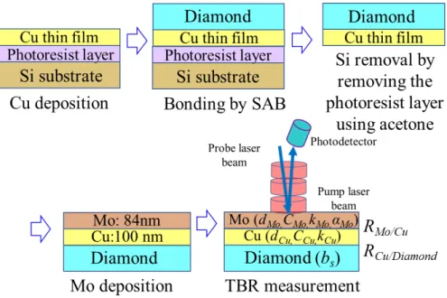
The TBR of the Cu/diamond bonding interface was measured by the time domain pulsed-light-heating thermoreflectance technique.25 A thin-Cu/diamond bonding structure was fabricated to
investigate the TBR of the bonding interface. First, a thin Cu film was deposited onto the photoresist layer coating the Si substrate by electron beam evaporation (EBE). The evaporation-deposited Cu film and diamond substrate were bonded by SAB, and then the Si substrate was removed by removing the photoresist layer using acetone. Finally, a thin Mo film was evaporated onto the Cu bonded to diamond by EBE, as shown in Figure 1. The thicknesses of the Cu and Mo thin films were measured to be 100 and 99 nm, respectively, by a Stylus Profiler (Alpha-Step D-500) with a high resolution of 0.038 nm. In addition, Cu and Mo thin films with the same thickness were evaporated separately onto a diamond substrate and were used as references.
6
The measurement system consisted of a pump laser and a probe laser, as shown in Figure 1. The repetition rate, wavelength, optical power, and spot radius of the pump laser were 20 MHz, 1550 nm, 30 mW, and 70 μm, respectively. The same parameters of the probe laser were 20 MHz, 775 nm, 1.5 mW, and 15 μm, respectively. A Mo film was employed as a transducer film. The pump laser with an intensity modulation of 200 kHz was used to irradiate the Mo film surface. The probe laser beam was focused on the same irradiation spot, with a specific time delay controlled by an arbitrary function generator. The reflected probe laser beam was detected by a photodetector. The transient temperature of the heated area was detected as the phase signal of a lock-in amplifier.26 The signal was recorded as
a function of the delay time of the probe laser pulse relative to the pump laser pulse, which was 10 ns. The transient temperature curve depends on the thermophysical properties of the layers and the TBR between layers through which the heat flow passe. Here, d is the film thickness, C is the volumetric heat capacity, κ is the thermal diffusivity, α is the absorption coefficient, b is the thermal effusivity, and
R is the TBR. Since the diameters of the laser spots are more than 100 times larger than the film
thickness, one-dimensional heat conduction can be assumed during data analysis using a lock-in signal simulation for the thermal reflectance measurement.27
RESULTS AND DISCUSSION
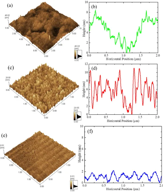
The three-dimensional AFM images and the corresponding cross-sectional profiles of the Cu plate, the deposited Cu thin film, and the diamond substrate surface are shown in Figures2(a) and 2(b), 2(c)
7
and 2(d), and 2(e) and 2(f), respectively. The average roughness (Ra) values of the Cu, the deposited Cu thin film, and the diamond substrate surface were determined to be 2.4, 1.9 and 0.4 nm, respectively. The differences between the peaks and valleys of the Cu plate, the deposited Cu thin film, and the diamond substrate surface were determined to be approximately 8.5, 10.8 and 2.2 nm, respectively. The Cu plate used in the experiment was manufactured by the roller rolling method, so the surface roughness was rather high. In addition, the surface of the deposited Cu thin film was also very rough, and the main reason for this effect could be attributed to the rough surface of the photoresist layer coating the Si. The diamond surface had been polished, so its surface was extremely flat. The surface roughness of bonding materials is a critical factor in wafer direct bonding at room temperature. Bonding materials with nano-level flatness will largely produce a lower formation of voids, which efficiently increases the bonding strength. Although the Cu surface was rougher, it easily deformed when a large pressure was applied. Therefore, although the Cu plate and the deposited Cu thin film had large Ra values describing the surface roughness, it was still possible to bond both directly to diamond.
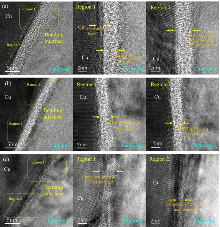
Figures 3(a), 3(b), and 3(c) show cross-sectional STEM images of the as-bonded Cu/diamond interface and the interfaces annealed at 500 and 700 ℃, respectively. The microstructure of the bonding interface was visible. No structural defects or nanovoids were observed at the interfaces, even after annealing at the high temperature of 700 ℃. A sharp interface and an approximately 4.5 nm thick intermediate layer were observed at the as-bonded Cu/diamond interface [Figure 3(a)]. Some lattice
8
fringes of Cu and diamond arranged coherently across the interface were observed. This result indicates that the intermediate layer was composed of a crystal defect layer of Cu and diamond. The thicknesses of the crystal defect layers of Cu and diamond were measured to be approximately 1.5 and 3 nm, respectively. After annealing at 500 ℃, no Cu crystal defect layer was observed, and the thickness of the diamond crystal defect layer decreased to approximately 2 nm. Furthermore, when the annealing temperature was increased to 700 °C, no diamond crystal defect layer was observed at the interface. Instead of the crystal defect layer, a mating layer composed of Cu and diamond with a thickness of approximately 3 nm was observed at the interface [Figure 3(c)]. The thickness of the defect layer and the mating layer was nonuniform, which should have been related to the roughness values of the Cu and diamond surfaces.
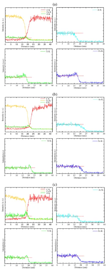
The X-ray intensity profiles of the C, Cu, O, Ar, Ti, and Fe atoms across the as-bonded Cu/diamond interface and the interfaces annealed at 500 and 700 ℃ are shown in Figures 4(a), 4(b), and 4(c), respectively. The red dotted line shows the average intensity of the background noise. For the O, Ar, T, and Fe atoms, the X-ray intensity near the interface was clearly higher than that at the position separated from the interface, which indicates that the O, Ar, T, and Fe atoms were distributed in the interface. O and Ar atoms were detected at the as-bonded interface and were at the background level. Small signal peaks from Ti and Fe atoms were observed at the as-bonded interface, which could have been due to contaminants that formed from the metal vacuum chamber during the activation process. After annealing at 500 ℃, the signal peak of Ti atoms was still observed at the interface. In addition,
9
a small signal peak of O atoms was also observed at the interface. However, no signal peak of Fe atoms was observed at the interface. This observation could have been because the concentration of Fe atoms distributed at the interface was below the resolution of the detector sensor due to diffusion after annealing. When the annealing temperature increased to 700 ℃, the signal peak intensity of O atoms became stronger [Figure 4(c)]. However, no a change was observed in the peak intensity of Ti atoms. The enhancement of the O atom peak intensity could be attributed to the increase in the concentration of O atoms distributed near the interface after annealing. This result indicated that an oxide layer was formed at the 700 ℃ annealed interfaces. For the Ar atoms, no signal peak was observed at the as-bonded interface or at the interfaces annealed at 500 and 700 ℃, which indicated that the concentration of Ar atoms distributed at the interface was exceptionally low.
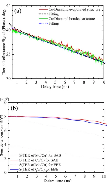
Figures 5(a) shows the thermal reflectance signals (solid lines) of the Cu/diamond interfaces prepared by the SAB and EBE methods. Fittings of the thermoreflectance signals were performed within the range of 0.2 – 50 ns using a simulated lock-in thermoreflectance signal (solid circle) to obtain the TBR between the Cu and diamond. Then, the simulated signals had a good agreement with experimental signals between 0.5 and 10 ns for both SAB and EBE cases. The parameters used in the fittings are shown in Table I. The thermal diffusivity and the thermal conductivity of the Mo thin film were determined to be 2.1×10⁻⁶ m2/S and 0.053 W/cm∙K, respectively, by determining an 99nm thick Mo
thin film evaporated onto a quartz substrate using the rear heating/front detection type pulsed light heating time-domain thermal reflectance technique.28 The TBR between Mo and Cu was obtained to
10
be approximately 1.4×10⁻⁸ m2∙K/W, which is significantly larger than the previously reported value.29
The reason is that there were not enough electron carriers. Since the obtained thermal diffusivity value of the Mo thin film is very small, the Mo thin film should be oxidized. In addition, the surface of Cu bonded to diamond was exposed to the atmosphere prior to deposition of the Mo film, so an oxide layer could have formed on the Cu surface, which may have caused thermal resistance. The TBR values of the Cu/diamond interfaces prepared by SAB and EBE were determined to be both 1.7×10⁻⁸ m2∙
K/W. Furthermore, the obtained TBR values of the Cu/diamond interface are in good agreement with the value of 1.13×10⁻⁸ m2∙K/W calculated by the phonon diffuse mismatch model.30
The absolute values of sensitivity around best fitted value of unknown parameters are shown in Figure 5(b). The difference between sensitivities of TBR of Cu/diamond and that of TBR of Mo/Cu is little. Therefore, both unknown parameters (TBR of Mo/Cu and TBR of Cu/diamond) can be determined. Uncertainties of TBR (𝑢𝑢𝑇𝑇𝑇𝑇𝑇𝑇) for Mo/Cu interface and Cu/diamond are calculated using the law of
propagation of uncertainty, that is following equation:
𝑢𝑢𝑇𝑇𝑇𝑇𝑇𝑇 = �𝑢𝑢𝑀𝑀𝑀𝑀_𝑇𝑇𝑇𝑇2 + 𝑢𝑢𝑀𝑀𝑀𝑀_𝑑𝑑2 + 𝑢𝑢𝑇𝑇𝐷𝐷𝐷𝐷𝐷𝐷𝑀𝑀𝐷𝐷𝑑𝑑_𝑇𝑇𝑇𝑇2 +𝑢𝑢𝑓𝑓𝐷𝐷𝑓𝑓𝑓𝑓𝐷𝐷𝐷𝐷𝑓𝑓2
where 𝑢𝑢𝑀𝑀𝑀𝑀_𝑇𝑇𝑇𝑇 , 𝑢𝑢𝑀𝑀𝑀𝑀_𝑑𝑑 , 𝑢𝑢𝑇𝑇𝐷𝐷𝐷𝐷𝐷𝐷𝑀𝑀𝐷𝐷𝑑𝑑_𝑇𝑇𝑇𝑇 , and 𝑢𝑢𝑓𝑓𝐷𝐷𝑓𝑓𝑓𝑓𝐷𝐷𝐷𝐷𝑓𝑓 are TBR uncertainties coming from thermal
diffusivity of Molybdenum, thickness of Molybdenum, thermal effusivity of Diamond and standard deviation on fitting results when the best fit case, respectively. Consequently, we report TBR values with the expanded uncertainty with conversion factor (k = 2) as shown in the Table Ⅱ. Uncertainties of TBR for the Cu/diamond interfaces prepared by SAB and EBE were determined to be ± 0.2×10⁻⁸ and
11
± 0.3×10⁻⁸ m2∙K/W, respectively.
We found that the crystal defect layer formed at the as-bonded Cu/diamond interface was unlike those in previous reports involving SAB-fabricated Si/Si,31 Si/GaAs,32 and Si/SiC33 interfaces.It is generally
believed that the amorphous layer is formed at the bonding interface due to excessive Ar beam irradiation during the bonding process. However, not all materials irradiated by the Ar beam will become amorphous. It has been reported that a very thin crystal defect layer was induced at the GaAs/GaAs34 and Cu/Cu35 homointerfaces fabricated by SAB.An GaAs crystal defect layer and an
a-Si amorphous layer were formed at the GaAs and a-Si sides of the bonding interface, respectively, as reported.34 These results indicate that Ar beam-irradiation will induce a partial crystal defect at the Cu
and diamond bonding surfaces.
No oxygen atoms were detected at the as-bonded interface, which is different from the result previously reported for an Al/diamond interface.23 This result could have occurred because no oxide
layer was formed at the interface or because the concentration of O atoms distributed at the interface was too low to detect. The oxidation temperature of copper is higher than 300 °C under atmospheric ambient conditions.36 Therefore, it is difficult for the Cu surface irradiated by the Ar beam to
immediately react with the residual oxygen in the vacuum chamber to form a copper oxide at room temperature. As the annealing temperature increases, the O atoms distributed at the interface will be concentrated. The concentrated O atoms will react with Cu to form copper oxide. The oxide layer observed in the X-ray intensity profile of the 700 ℃ annealed interfaces should be this copper oxide
12
layer.
It is important to note that the difference between the thermal expansion coefficients of Cu (16.42 × 10⁻⁶/K) and diamond (2.3 × 10⁻⁶/K) is very large, while no mechanical phenomena, such as cracks or
interface separation, were observed at the annealed interface. This result implies that the bonding interface with a high thermal stability could be related to the structural properties of the composite layer formed at the interface. The Cu and diamond surfaces had nano-level roughness, so nanovoids should have been formed at the bonding interface. However, no nanovoids were observed at the interface. This result could have occurred due to the plastic deformation of the Cu bonding surface. The Cu and diamond surfaces made intimate contact to form a nano-level composite interface. The structure of the composite interface was difficult to identify by STEM observation due to the crystal defect layer formed at the interface. After annealing at 700 °C, the crystal defect layer was recovered, so the structure of the composite layer could be recognized. The recovery of the crystal defect layer was very similar to the findings in previous reports, indicating that the damaged layer formed at the interface by Ar beam irradiation can be recrystallized through a high-temperature annealing process.35,37,38
The thermal expansion coefficient of the composite layer composed of Cu and diamond should be different from those of the bulk diamond and Cu. It has been reported that the thermal expansion coefficient of the composite material composed of Cu and diamond highly depends on the component ratio between diamond and Cu, decreasing with increasing amounts of the diamond component.39 The
13
composite layer played a role in relieving the residual stress generated by the difference in the thermal expansion coefficients between diamond and Cu. Similar results have been reported for a diamond/Si interface fabricated by SAB, wherein a SiC intermediate layer was formed at the 1000 °C annealed interface to play a role in relaxing the residual stress.40 In addition, copper oxide is well known to have
a low thermal expansion coefficient (Cu2O: 1.8 ~ 2.8 × 10⁻⁶/K and CuO: 5.9 × 10⁻⁶/K) at room
temperature.41,42 The copper oxide formed at the interface could also play a role in reducing the stress
caused by the difference in the thermal expansion coefficients between Cu and diamond. A similar result has been reported, indicating that copper oxide formed at the defect sites of plasma-treated graphene played an efficient role in enhancing the load transfer and thermal stress relaxation between graphene and Cu matrixes.43,44
The thermal reflectance signals and fitting results were little off at times delay than 6 ns. From the sensitivities as shown in Fig. 5(b), the sensitivities over 6 ns are less than those under 6 ns. This result indicated that the deviation over 6 ns less affect the TBR values. The surface of the Cu thin film bonded to diamond exhibits substantial roughness. The difference between the peaks and valleys on the Cu thin film surface is about ± 15 nm, at best, according to the AFM image (Figure 2(d)). Even if the Cu film thickness changes from 84 nm to 114 nm, the thermal resistance of the Cu thin film was on the order of 10-10 m2∙K/W and is sufficiently smaller than the interfacial thermal resistance, so the effect
of surface roughness can be ignored. For the Mo thin film, since the thermal resistance of the Mo thin film is approximately 1.4 × 10⁻⁸ m2∙K/W, the effect of the Mo thin film roughness is quite large.
14
Importantly, the TBR value of the Cu/diamond bonded structure is the same as that of the Cu/diamond evaporated structure. These results suggest that the effect of the crystal defect layer formed at the interface on the phonon transport properties across the bonding interface is small and can be ignored.
The advantage of the Cu/diamond direct bonding using SAB compared to the deposition method is that can easily fabricate the bonding structure with a Cu plate thicker than 1 mm. Furthermore, the bonded structure can withstand for varying temperature ranging from room temperature to 700 ℃. This is difficult for the structure fabricated by the deposition method due to the difference in the thermal expansion coefficients of Cu and diamond. Furthermore, it will generally take a lot of time and production costs to deposit a thick metal film using the conventional coating method such as Electron Beam Evaporation and Sputter-Deposition. The direct bonding of diamond and Cu plate can also be achieved for diamond surface roughness larger than 1 nm under a pressure of 0.5 MPa. The Cu/diamond bonding interface with thermal stability at up to 700 ℃ is fully competent for use in addressing power-device temperature increases during operation. All the experimental results indicated that the direct bonding of diamond and Cu is an excellent technique by which to reduce the thermal resistance between diamond and Cu due to the absence of solder materials and is very useful in practical applications.
CONCLUSIONS
15
at room temperature were characterized by STEM and the time domain pulsed-light-heating thermoreflectance technique. No mechanical defects, such as cracks or voids, were observed at the interface, even at an annealing temperature of 700 ℃. An approximately 4.5 nm thick crystal defect layer consisting of diamond and Cu was formed at the as-bonded interface. The thickness of the crystal defect layer decreased as the annealing temperature increased. Finally, the crystal defect layer was recovered after annealing at 700 ℃. A mating interface layer and a copper oxide layer replacing the defect layer were observed at 700 ℃ annealed interfaces, which played a role in relieving the residual stresses caused by the different thermal expansion coefficients between diamond and Cu. The TBR value of the Cu/diamond bonded structure was determined to be 1.7± 0.2×10⁻⁸ m2∙K/W, which was
consistent with that of the Cu/diamond evaporated structure. These results indicated that the Cu/diamond interface prepared by SAB is highly useful for connecting diamond and heat sink materials for high-power applications.
AUTHOR INFORMATION Corresponding Author
*E-mail: [email protected]
16
This work was supported by the “Research and development of high thermal stability interface by direct bonding of diamond” project in the Feasibility Study Program of New Energy and Industrial Technology Development Organization (NEDO) (contract number: 19101242-0). The fabrication of the STEM samples and part of the STEM observations were respectively performed at The Oarai Center and at the Laboratory of Alpha-Ray Emitters in IMR under the Inter-University Cooperative Research in IMR of Tohoku University (NO. 18M0045 and 19M0037). STEM-EDS was performed at ISIR under the Cooperative Research Program of “Network Joint Research Center for Materials and Devices: Dynamic Alliance for Open Innovation Bridging Human, Environment and Materials” (No. 20191240).
REFERENCES
(1) Chu, K.; Jia, C.; Liang, X.; Chen. H.; Guo, H.; Yin, F. et al., Experimental and Modeling Study of the Thermal Conductivity of SiCp/Al Composites with Bimodal Size Distribution. J. Mater. Sci. 2009, 44, 4370 – 4378.
(2) Kida, M.; Weber, L.; Monachon, C.; Mortensen, A. Thermal Conductivity and Interfacial Conductance of AlN Particle Reinforced Metal Matrix Composites. J. Appl. Phys. 2011, 109, No. 064907.
Molina-17
Aldareguia, J. M.; Odén, M. Thermomechanical Properties of Copper-Carbon Nanofiber Composites Prepared by Spark Plasma Sintering and Hot Pressing. Compos. Sci. Technol. 2010, 70, 2263 – 2268. (4) Chu, K.; Wang, X. H.; Wang, F.; Li, Y. B.; Huang, D. J.; Liu, H.; Ma, W. L.; Liu, F. X.; Zhang, H. Largely Enhanced Thermal Conductivity of Graphene/Copper Composites with Highly Aligned Graphene Network. Carbon 2018, 127, 102 – 112.
(5) Chu, K.; Wang, X. H.; Li, Y. B.; Huang, D. J.; Geng, Z. R.; Zhao, X. L.; Liu, H.; Zhang, H. Thermal Properties of Graphene/Metal Composites with Aligned Graphene. Mater. Des. 2018, 140, 85 – 94. (6) Yamamoto, Y.; Imai, T.; Tanabe, K.; Tsuno, T.; Kumazawa, Y.; Fujimori, N. The Measurement of Thermal Properties of Diamond. Diam. Relat. Mater. 1997, 6, 1057 – 1061.
(7) Nosaeva, K.; Weimann, N.; Rudolph, M.; John, W.; Krueger, O.; Heinrich, W. Improved Thermal Management of InP Transistors in Transferred-Substrate Technology with Diamond Heat-Spreading Layer. Electron. Lett. 2015, 51, 1010 – 1012.
(8) Sun, H.; Simon, R. B.; Pomeroy, J. W.; Francis, D.; Faili, F.; Twitchen, D. J.; Kuball, M. Reducing GaN-on-Diamond Interfacial Thermal Resistance for High Power Transistor Applications. Appl. Phys.
Lett. 2015, 106, No. 111906.
(9) Francis, D.; Faili, F.; Babic, D.; Ejeckam, Nurmikko, F. A.; Maris, H. Formation and Characterization of 4-inch GaN-on-Diamond Substrates. Diamond Relat. Mater. 2012, 19, 229 – 233. (10) Pomeroy, J. W.; Bernardoni, M.; Dumka, D. C.; Fanning, D. M.; Kuball, M. Low Thermal
18
Thermography Mapping. Appl. Phys. Lett. 2014, 104, No. 083513.
(11) Hirama, K.; Taniyasu, Y.; Kasu, M. AlGaN/GaN High-Electron Mobility Transistors with Low Thermal Resistance Grown on Single-Crystal Diamond (111) Substrates by Metalorganic Vapor-Phase Epitaxy. Appl. Phys. Lett. 2011, 98, No.162112.
(12) Gerrer, T.; Cimalla, V.; Waltereit, P.; Müller, S.; Benkhelifa, F.; Maier, T.; Czap, H.; Ambacher, O.; Quay, R. Transfer of AlGaN/GaN RF-Devices onto Diamond Substrates Via Van Der Waals Bonding. International Journal of Microwave and Wireless Technologies 2018, 10, 666 – 673. (13) Wu, Q.; Xu, Y.; Zhou, J.; Kong, Y.; Chen, T.; Wang, Y.; Lin, F.; Fu, Y.; Jia, Y.; Zhao, X.; Yan, B.;
Xu, R. Performance Comparison of GaN HEMTs on Diamond and SiC Substrates Based on Surface Potential Model. ECS J. Solid State Sci. Technol. 2017,6, Q171 – Q178.
(14) Saura, A.; Ji, H.; Hilton, K. P.; Wallis, D. J.; Uren, M. J.; Martin, T.; Kuball, M. Thermal Boundary Resistance between GaN and Substrate in AlGaN/GaN Electronic Devices. IEEE Trans. Electron
Devices 2007, 54, 3152 – 3158.
(15) Du, M.; Guo, Q.; Ouyang, Z.; Wei, K.; Hurley, W. G. Effects of Solder Layer Crack on the Thermal Reliability of Insulated Gate Bipolar Transistors. Case Studied in Thermal Engineering 2019, 14, No. 100492.
(16) Jourdain, A.; Stoukatch, S.; De Moor, P.; and Ruythooren, W. Simultaneous Cu-Cu and Compliant Dielectric Bonding for 3D Stacking of ICs. Proc. IITC, 2007, 207 – 209.
19
Wavelength Lasers on a (110) GaAs Substrate by Direct Bonding (A Prospect for Free-Orientation Integration). Appl. Phys. Lett. 1995, 67, 810 – 812.
(18) Tan, C. M.; Yu, W.; and Wei, J. Comparison of Medium-Vacuum and Plasma-Activated Low-Temperature Wafer Bonding. Appl. Phys. Lett. 2006, 88, No. 114102.
(19) Liang, J.; Miyazaki, T.; Morimoto, M.; Nishida, S.; Watanabe, N.; Shigekawa, N. Electrical Properties of p-Si/n-GaAs Heterojunctions by Using Surface-Activated Bonding. Appl. Phys.
Express 2013, 6, No. 021801.
(20) Higurashi, E.; Okumura, K.; Nakasuji, K.; and Suga, T. Surface Activated Bonding of GaAs and SiC Wafers at Room Temperature for Improved Heat Dissipation in High-Power Semiconductor Lasers. Jpn. J. Appl. Phys. 2015, 54, No. 030207.
(21) Liang, J.; Masuya, S.; Kasu, M.; Shigekawa, N. Realization of Direct Bonding of Single Crystal Diamond and Si Substrates. Appl. Phys. Lett. 2017, 110, No.111603.
(22) Sakata, M.; Oyake, T.; Maire, J.; Nomura, M.; Higurashi, E.; and Shiomi, J. Thermal Conductance of Silicon Interface Directly Bonded by Room-Temperature Surface Activation. Appl. Phys. Lett. 2015, 106, No. 081603.
(23) Liang, J.; Yamajo, S.; Kuball, M.; Shigekawa, N. Room-Temperature Direct Bonding of Diamond and Al. Scripta Mater. 2019, 159, 58 – 61.
(24) Kanda, S.; Shimizu, Y.; Ohno, Y.; Shirasaki, K.; Nagai, Y.; Kasu, M.; Shigekawa, N.; Liang, J. Fabrication of Diamond/Cu Direct Bonding Interface for Power Device Applications. Jpn. J. Appl.
20 Phys. 2019, 59, No. SBBB03.
(25) Yamashita, Y.; Honda, K.; Yagi, T.; Jia, J.; Taketoshi, N.; Shigesato, Y. Thermal Conductivity of Hetero-Epitaxial ZnO Thin Films on C- and R-Plane Sapphire Substrates: Thickness and Grain Size Effect. J. Appl. Phys. 2019, 125, No. 035101.
(26) Taketoshi, N.; Baba, T.; Schaub, E.; Ono, A. Homodyne Detection Technique Using Spontaneously Generated Reference Signal in Picosecond Thermoreflectance Measurements. Rev. Sci.
Instrum. 2003, 74, No. 5226.
(27) T Yagi. Kobayashi, K. In Proceedings of the 35th Japan Symposium Thermophysical Properties. 2014 Japan Society of Thermophysical Properties Symposium (JSTP); 2014, pp 16 – 20 (in Japanese). (28) Taketoshi, N.; Baba, T.; Ono, A. Electrical Delay Technique in the Picosecond Thermoreflectance Method for Thermophysical Property Measurements of Thin Films. Rev. Sci, Instrum. 2005, 76, No. 094903.
(29) Chiristian, M.; Ludger, W. Thermal Boundary Conductance of Transition Metals on Diamond.
Emerging Materials Research 2012, 1, 89 – 98.
(30) Wang, H. Xu, Y. Shimono, M. Tanaka, Y. Yamazaki, M. Computation of Interfacial Thermal Resistance by Phonon Diffuse Mismatch Model. Materials Transactions 2007, 48, 2349 – 2352. (31) Liang, J.; Miyazaki, T.; Morimoto, M.; Nishida, S.; Shigekawa, N. Electrical Properties of Si/Si Interfaces by Using Surface-Activated Bonding. J. Appl. Phys. 2013, 114, No. 183703.
21
Resistance of Si/GaAs Heterojunctions Fabricated by Surface-Activated Bonding. Jpn. J. Appl. Phys. 2015, 54, No. 030211.
(33) Liang, J.; Nishida, S.; Arai, M.; Shigekawa, N. Effects of Thermal Annealing Process on the Eectrical Properties of p+-Si/n-SiC Heterojunctions. Appl. Phys. Lett. 2014, 104, No. 161604.
(34) Ohno, Y.; Yoshida, H.; Takeda, S.; Liang, J.; Shigekawa, N. Intrinsic Microstructure of Si/GaAs Heterointerfaces Fabricated by Surface-Activated Bonding at Room Temperature. Jpn. J. Appl. Phys. 2018, 57, No. 02BA01.
(35) Kim, T.; Howlader, H. M. M.; Itoh, R. T.; Suga, T. Room Temperature Cu–Cu Direct Bonding Using Surface Activated Bonding Method. J. Vac. Sci. & Technol. A 2003, 21, No. 449.
(36) Lee, S.; Hsu, H.; Tuan, W. Oxidation Behavior of Copper at a Temperature below 300 ℃ and the Methodology for Passivation. Mat. Res. 2016, 19, 51 – 56.
(37) Howlader, M. M. R.; Zhang, F. Void-Free Strong Bonding of Surface Activated Silicon Wafers from Room Temperature to Annealing at 600°C. Thin Solid Films 2010, 519, 804 – 808.
(38) Yamajo, S.; Yoon, S.; Liang, J.; Sodabanlu, H.; Watanabe, K.; Sugiyama, M.; Yasui, A.; Ikenaga, E.; Shigekawa, N. Hard X-Ray Photoelectron Spectroscopy Investigation of Annealing Effects on Buried Oxide in GaAs/Si Junctions by Surface-Activated Bonding. Appl. Surf. Sci. 2019, 473, 627 – 632.
(39) Liang, J.; Masuya, S.; Kim, S.; Oishi, T.; Kasu, M.; Shigekawa, N. Stability of Diamond/Si Bonding Interface During Device Fabrication Process. Appl. Phys. Express 2019, 12, No. 016501.
22
(40) Guillemet, T.; Geffroy, P. M.; Heintz, J. M.; Chandra, N.; Lu, Y. F.; Silvain, J. F. An Innovative Process to Fabricate Copper/Diamond Composite Films for Thermal Management Applications.
Composites Part a: Applied Science and Manufacturing 2012, 43, 1746 – 1753.
(41) Liang, J.; Zhou, Y.; Masuya, S.; Gucmann, F.; Singh, M.; Pomeroy, J.; Kim, S.; Kuball, M.; Kasu, M.; Shigekawa, N. Annealing Effect of Surface-Activated Bonded Diamond/Si Interface. Diam. Relat.
Mater. 2019, 93, 187 – 192.
(42) Suzuki, T. X-Ray Study on the Binding Properties of Cu2O and Ag2O Crystals. J. Phys. Soc. Jpn.
1960, 15, 2018 – 2024.
(43) Chu, K.; Wang, J.; Liu, Y. P.; Geng, Z. R. Graphene Defect Engineering for Optimizing the Interface and Mechanical Properties of Graphene/Copper Composites. Carbon 2018, 140, 112 – 123. (44) Chu, K.; Wang, J.; Liu, Y. P.; Li, Y. B.; Geng, Z. R.; Zhang, H. Creating Defects on Graphene Basal-Plane Toward Interface Optimization of Graphene/CuCr Composites. Carbon 2019, 143, 85 – 96.
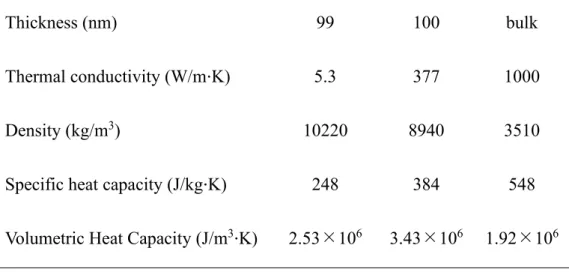
Table I. Parameters used in the lock-in thermal reflectance signal simulation.
23
Thickness (nm)
Thermal conductivity (W/m∙K) Density (kg/m3)
Specific heat capacity (J/kg∙K) Volumetric Heat Capacity (J/m3∙K)
99 5.3 10220 248 2.53×10⁶ 100 377 8940 384 3.43×10⁶ bulk 1000 3510 548 1.92×10⁶
Table Ⅱ. TBR with uncertainties for Mo/Cu and Cu/diamond interfaces. TBR of Mo/Cu TBR of Cu/diamond SAB 1.4 ± 0.4×10⁻⁸ m2∙K/W 1.7 ± 0.2×10⁻⁸ m2∙K/W
24
Figure 1. Schematic diagram of the fabrication of thin-Cu/diamond bonded structures and measurement of the TBR.
25
Figure 2. AFM images and corresponding cross-sectional profiles of the Cu plate (a) and (b), the deposited Cu thin film (c) and (d), and the diamond substrate (e) and (f) surfaces.
26
Figure 3. Cross-sectional STEM images of the as-bonded Cu/diamond interface (a) and the interfaces annealed at 500 (b) and 700 ℃ (c).
27
Figure 4. X-ray intensity profiles of C, Cu, O, Ar, Ti, and Fe in the as-bonded Cu/diamond interface (a) and the interfaces annealed at 500 (b) and 700 ℃ (c). The red dotted line shows the average
28
intensity of the background noise.
Figure 5. Thermal reflectance signals (solid line) and fitting results (solid circle) for delay times ranging from 0.5 to 10 ns for the as-bonded Cu/diamond structure and the Cu/diamond evaporated structure as a reference (a) and sensitivity as a function of delay times for TBRs of Mo/Cu interfaces
and Cu/diamond interfaces (b).
1 2 3 4 5 6 7 8 9 10 30 35 40 45
(a)
Th er m al ref lect an ce S ig nal (P hase) . d eg . Delay time (ns)Cu/Diamond evaporated structure Fitting
Cu/Diamond bonded structure Fitting 1 2 3 4 5 6 7 8 9 10 0 2 4 6 8 10 S ens it iv it y, d eg ./( m 2 ⋅K/W ) Delay time (ns)
S(TBR of Mo/Cu) for SAB S(TBR of Cu/C) for SAB S(TBR of Mo/Cu) for EBE S(TBR of Cu/C) for EBE
[×108]
29