Subnitride and valence band offset at Si3N4/Si
interface formed using nitrogen-hydrogen
radicals
著者
寺本 章伸
journal or
publication title
Applied Physics Letters
volume
90
number
12
page range
123114-1-123114-3
year
2007
URL
http://hdl.handle.net/10097/47980
doi: 10.1063/1.2715037Subnitride and valence band offset at Si
3N
4/ Si interface formed using
nitrogen-hydrogen radicals
Masaaki Higuchi and Shigetoshi Sugawa
Graduate School of Engineering, Tohoku University, Aza-Aoba, Aramaki, Aoba-ku, Sendai 980-8579, Japan
Eiji Ikenaga
JASRI/Spring-8, Kouto, Mikazuki, Hyogo, 679-5198, Japan
Jiro Ushio
Advanced Research Laboratory, Hitachi Ltd., Hitachi-shi, Ibaraki 319-1292, Japan
Hiroshi Nohira and Takuya Maruizumi
Musashi Institute of Technology, Tamazutsumi, Setagaya-ku, Tokyo 158-8857, Japan
Akinobu Teramoto,a兲Tadahiro Ohmi, and Takeo Hattori
New Industry Creation Hatchery Center, Tohoku University, Aza-Aoba, Aramaki, Aoba, Sendai 980-8579, Japan
共Received 19 September 2006; accepted 13 February 2007; published online 22 March 2007兲 The authors measured soft x-ray-excited angle-resolved photoemission from Si 2p, N 1s, and O 1s core levels, and valence band for nitride films formed on Si共100兲, Si共111兲, and Si共110兲 using nitrogen-hydrogen radicals with the same probing depth. The Si3N4/ Si interfaces formed exhibited an almost abrupt compositional transition. Furthermore, the crystal orientation of Si substrate affects the total areal density of subnitrides but not the valence band offset at the Si3N4/ Si interface. © 2007 American Institute of Physics.关DOI:10.1063/1.2715037兴
High- gate dielectrics with a low leakage current are highly anticipated for advanced ultralarge scale integrations 共ULSIs兲.1
Si3N4 film formed using nitrogen-hydrogen共NH兲
radicals is attractive as a high- gate dielectric owing to its high relative dielectric constant共7.5兲 and low interface state density.2,3Hayafuji and Kajiwara found that during the ther-mal nitridation of Si共100兲 in NH3 nitride-film growth is in-dependent of NH3 pressure.4 Maillot et al.5 proposed
pos-sible atomic transport mechanisms during the thermal nitridation of Si in NH3using 15N. From the photoemission
arising from Si 2p and N 1s core levels in thin nitride films grown in situ by the high-temperature reaction of Si共100兲 with NH3, Peden et al. found that a Si monolayer exists as
the outermost surface layer on top of a Si3N4film.6
Because the Si3N4 film required for advanced ULSIs must be ultrathin, the characterization and control of the Si3N4/ Si interface structure on an atomic scale are essential.
Because the thickness of the nitride films is more than 1 nm, an electron escape depth of nearly 2 nm and highly brilliant synchrotron radiation are necessary in detecting the photo-emission from the Si3N4/ Si interface through the Si3N4film, and a high energy resolution of 100 meV is necessary to resolve the intermediate nitridation states of Si共abbreviated hereafter as subnitrides兲 localized at the Si3N4/ Si interface.
Furthermore, to detect subnitride and valence band offset with the same probing depth in addition to simply determine the compositional depth profile, the kinetic energies, which govern the electron escape depths,7of photoelectrons emitted from Si 2p, N 1s, and O 1s core levels, and the valence band were adjusted to be equal by choosing appropriate photon energies for each core level and valence band. Such measure-ments could be performed at Super Photon Ring 8 GeV 共SPring-8兲.
The wafers used in this study are n-type Si共100兲, Si共111兲, and Si共110兲 substrates. The atomically smooth sub-strates were prepared by the following processes. The wet oxidation of these substrates was performed at 1100 ° C to form 1-m-thick oxide films. After etching the oxide films in HCl/ HF mixture solution,8 the substrates were cleaned in five steps at room temperature.9After cleaning, the surface microroughness共Ra兲 of these cleaned substrates measured by
atomic force microscopy was 0.08 nm. Then, the nitridation of these substrates using NH radicals produced in a microwave-excited high-density Xe/ NH3 mixture plasma10
was performed at a pressure of 20 Pa and substrate tempera-ture of 600 ° C, and the nitride films thus formed were kept in dry N2 until their photoelectron spectra were measured.
The microwave frequency and power were 2.45 GHz and 5 W / cm2, respectively.
Figures 1共a兲 and1共b兲 show the N 1s and O 1s spectra arising from the nitride film formed on the Si共100兲 surface measured at a photoelectron take-off angle共TOA兲 of 52° and photon energies 共PEs兲 of 1349 and 1481 eV, respectively. The value of 397.3 eV observed for the binding energy共BE兲 of the N 1s spectrum peak indicates that most of the N atoms contribute to form Si3N4.6 The value of 532.2 eV observed for the BE of the O 1s spectrum peak indicates that all O atoms contribute to form Si–O–Si bonds.11 Si–O–Si bonds were formed by the oxidation of pure Si layer, which exists on the surface of a Si3N4 film after the nitridation of Si,6in
air just after the nitride film was removed from the nitrida-tion chamber. Figure 1共c兲 shows the intensity ratio
I共O 1s兲/I共N 1s兲 as a function of TOA. Here, I共O 1s兲 and I共N 1s兲 denote O 1s and N 1s spectral intensities,
respec-tively. The experimental data in Fig.1共c兲can be explained by the solid line calculated for the SiO2/ Si3N4/ Si共100兲
struc-ture. Here, the values of 0.52 and 1.05 nm were used for the thickness of the SiO2 layer and that of the Si3N4 layer,
re-a兲Electronic mail: [email protected]
APPLIED PHYSICS LETTERS 90, 123114共2007兲
0003-6951/2007/90共12兲/123114/3/$23.00 90, 123114-1 © 2007 American Institute of Physics
spectively. The other parameters used in the calculation of the solid line are discussed later. Furthermore, the N 1s spec-trum can be decomposed into a large peak with a low BE of 397.3 eV and a small peak with a high BE of 398.3 eV. The intensities of the large and small peaks are denoted by
I共N 1s, LBE兲 and I共N 1s, HBE兲, respectively. According to
a theoretical study of the BE of the N 1s core level,12a small peak can be correlated with a N atom that has three Si atoms as its first nearest neighbors and three N atoms and six O atoms as its second nearest neighbors, and hereafter referred to as an interface N atom because of the following reason. The dependence of I共N 1s, HBE兲/I共N 1s, LBE兲 on TOA in Fig.1共c兲can be explained by the broken line calculated for the N atoms having an areal density of 4.4⫻1018 m−2
local-ized at the SiO2/ Si3N4interface.
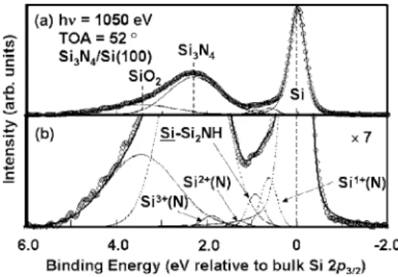
Figure2共a兲shows the Si 2p3/2spectrum arising from the
nitride film formed on Si共100兲 measured at a TOA of 52° and a PE of 1050 eV. Here, in the decomposition of the Si 2p spectrum, it was assumed that the spin-orbit splitting of the Si 2p spectrum is 0.608 eV and the Si 2p1/2 to Si 2p3/2
in-tensity ratio is 0.5.13 Other analytical details were described elsewhere.14 Figure 2共a兲is magnified sevenfold to result in Fig.2共b兲. In addition to the spectra expressed with Gaussian
functions arising from the SiO2, Si3N4, and Si substrates in
Fig.2共a兲, the spectra arising from four types of subnitrides, Si1+共N兲, Si2+共N兲, Si3+共N兲, and Si–Si
2NH were detected, as
shown in Fig.2共b兲. Here, Si1+共N兲 denotes a Si atom bonded with one N atom and three Si atoms, Si2+共N兲 denotes a Si atom bonded with two N atoms and two Si atoms, Si3+共N兲
denotes a Si atom bonded with three N atoms and one Si atom, and Si– Si2NH, which was theoretically shown to exist
at the Si3N4/ Si interface,15 denotes a Si atom bonded with
two Si atoms, one N atom, and one H atom. The chemical shifts 共CSs兲 of Si1+共N兲 and Si2+共N兲 agree with the reported values.6 The relatively small value of 2.25– 2.28 eV ob-served for the CS of the Si 2p core level in Si3N4 must be attributed to the decrease in its CS, in accordance with the decrease in the thickness of the Si3N4layer as in the case of
SiO2.16
Figure3 shows intensity ratios I共I兲/I共N兲 and I共O兲/I共N兲
as a function of TOA measured at a PE of 1050 eV for the nitride films formed on Si共100兲, Si共111兲, and Si共110兲. Here,
I共I兲, I共N兲, and I共O兲 denote the intensities of the Si 2p3/2
spectrum arising from all subnitrides, that arising from Si3N4, and that arising from SiO2, respectively. The experi-mental data in Fig.3can be explained by the solid and bro-ken lines calculated for the SiO2/ Si3N4/ subnitride/ Si
struc-ture using the following parameters. Here, the experimental data in Fig.1共c兲and those in Fig.3 are not affected by the photoelectron diffraction17 because SiO2 and Si3N4 are in
amorphous states and the subnitrides formed using NH radi-cals are randomly oriented in contrast to thermally grown silicon suboxides.18 The values of 6.08⫻1018, 5.80⫻1018,
and 5.59⫻1018m−2 were used for the total areal density of
subnitrides formed on Si共100兲, Si共111兲, and Si共110兲, respec-tively. The values of 2.86 and 2.41 nm were used for the electron escape depth in the SiO2 layer and that in Si3N4
layer, respectively. The values of 0.50 and 1.09 nm for Si共111兲, and the values of 0.52 and 1.11 nm for Si共110兲 were used for the thickness of the SiO2layer and that of the Si3N4
layer, respectively. The values of 2.28⫻1028m−3 and 3.19
⫻103kg m−3were used for the atomic concentration19 of Si in SiO2 and the density5 of Si3N4, respectively. The photo-ionization cross section of Si 2p core levels in the Si3N4
layer and that in the Si substrate are assumed to be the same. Because the total areal density of subnitrides formed on Si共100兲, Si共111兲, and Si共110兲 is smaller than the areal density of Si atoms on Si共100兲 共6.8⫻1018/ m2兲, Si共111兲 共7.85
⫻1018/ m2兲, and Si共110兲 共9.6⫻1018/ m2兲, respectively, the FIG. 1.共a兲 N 1s spectrum and 共b兲 O 1s spectrum measured at a TOA of 52°
and Pes of 1349 and 1481 eV for nitride film formed on Si共100兲, respec-tively. 共c兲 Intensity ratios I共O 1s兲/I共N 1s兲 and I共N 1s, HBE兲/ I共N 1s, LBE兲 as function of TOA. Here, I共O 1s兲 and I共N 1s兲 denote the intensities of the N 1s and O 1s spectra, respectively, and I共N 1s, HBE兲 and I共N 1s, LBE兲 denote the intensities of the high BE part and low BE part of the N 1s spectrum, respectively.
FIG. 2. 共a兲 Si 2p3/2 spectrum measured at a TOA of 52° and a PE of 1050 eV for the nitride film formed on Si共100兲. 共b兲 Part 2共a兲 is magnified sevenfold to indicate the resolved subnitride spectra.
FIG. 3.共a兲 Spectral intensity ratios I共I兲/I共N兲 and I共O兲/I共N兲 as a function of TOA measured at a PE of 1050 eV for the nitride film formed on Si共100兲, 共b兲 those on Si共111兲, and 共c兲 those on Si共110兲.
123114-2 Higuchi et al. Appl. Phys. Lett. 90, 123114共2007兲
compositional transition must be almost abrupt at the three Si3N4/ Si interfaces. Furthermore, the full widths at half maximum共FWHMs兲 of Si 2p spectra arising from Si sub-strate observed for Si共100兲, Si共111兲, and Si共110兲 are 0.409, 0.395, and 0.392 eV, respectively. Therefore, the total areal density of subnitrides and the FWHM of Si 2p spectrum arising from Si substrate decrease with the approaching of the areal density of Si on the Si substrate surface to that in Si3N4layer共1.17⫻1019/ m2兲.
Figure 4 shows the valence band 共VB兲 spectra arising from the nitride films formed on Si共100兲, Si共111兲, and Si共110兲 measured at TOAs of 15° and 80° and a PE of 951 eV. The VB spectra arising from the Si3N4films shown
in Fig.4 were obtained by subtracting the VB spectra mea-sured at a TOA of 80° from the VB spectra meamea-sured at a TOA of 15°, to eliminate the VB spectra arising from the Si substrate after multiplying the VB spectra arising from Si substrate measured at a TOA 15° by factors indicated in the figure. Consequently, the discontinuities of the valence band maximum 共VBM兲 of the Si substrate with respect to the VBM of the Si3N4 film, in other words, the valence band offsets 共⌬EV兲 at the Si3N4/ Si共100兲, Si3N4/ Si共111兲, and
Si3N4/ Si共110兲 interfaces, were determined to be 1.63±0.05,
1.63± 0.05, and 1.62± 0.06 eV, respectively. Therefore,⌬EV,
which is affected by the interface dipole at the interface,20is independent of the crystal orientation of Si substrate. This implies that the interface dipole formed using NH radicals is randomly oriented to result in the same sum of the interface dipole moment for three crystal orientations of Si substrate although the total areal density of subnitrides is dependent on the crystal orientation of Si substrate. Here, the VB spectra
arising from the nitride films, which were measured at a TOA of 80°, magnified 20-fold and those arising from Si3N4
magnified tenfold, were also shown to clearly indicate the VBMs of these spectra.
In conclusion, we measured the angle-resolved photo-emission from the Si 2p, N 1s, and O 1s core levels, and the valence band for the nitride films formed on Si共100兲, Si共111兲, and Si共110兲 using NH radicals with the same probing depth. It was found that almost abrupt compositional transitions oc-cur at the three Si3N4/ Si interfaces. Furthermore, it was
found that the crystal orientation of Si substrate affects the total areal density of subnitrides but not the valence band offset at the Si3N4/ Si interface.
The authors gratefully acknowledge the Ministry of Economy, Trade, and Industry and The New Energy and In-dustrial Technology Development Organization for their fi-nancial support to the development of plasma-process equip-ment. The synchrotron radiation experiments were performed at SPring-8 with the approval of the Japan Syn-chrotron Radiation Research Institute for the project of Nanotechnology Support of the Ministry of Education, Cul-ture, Sports, Science and Technology of Japan.
1G. D. Wilk, R. M. Wallace, and J. M. Anthony, J. Appl. Phys. 89, 5243 共2001兲.
2K. Sekine, Y. Saito, M. Hirayama, and T. Ohmi, IEEE Trans. Electron Devices 47, 1370共2000兲.
3H. Shimada, I. Ohshima, S. Nakao, M. Nakagawa, K. Kanemoto, M. Hirayama, S. Sugawa, and T. Ohmi, Tech. Dig. VLSI Symp. 2001, 67. 4Y. Hayafuji and K. Kajiwara, J. Electrochem. Soc. 129, 2102共1982兲. 5C. Maillot, H. Roulet, G. Dufour, F. Rochet, and S. Rigo, Appl. Surf. Sci.
26, 326共1986兲.
6C. H. F. Peden, J. W. Rogers, Jr., N. D. Shinn, K. B. Kidd, and K. L. Tsang, Phys. Rev. B 47, 15622共1993兲.
7S. Tanuma S, C. J. Powell, and D. R. Penn, Surf. Interface Anal. 20, 77 共1993兲.
8Y. Morita and H. Tokumoto, Appl. Surf. Sci. 100, 440共1996兲. 9T. Ohmi, J. Electrochem. Soc. 143, 2957共1996兲.
10Masaki Hirayama and Tadahiro Ohmi, The 1997 Joint International Meet-ing, Paris, August–September 1997共unpublished兲, Vol. 97-2, pp. 1802– 1803.
11F. J. Grunthaner, P. J. Grunthaner, R. P. Vasquez, B. F. Lewis, J. Maserjian, and A. Madhukar, Phys. Rev. Lett. 43, 1683共1979兲.
12H. Nohira, N. Tamura, J. Ushio, and T. Hattori, Proc.-Electrochem. Soc. 2005-01, 19共2005兲.
13F. J. Himpsel, F. R. McFeely, A. Talev-Ibrashimi, J. A. Yarmoff, and G. Hollinger, Phys. Rev. B 38, 6084共1988兲.
14K. Ohishi and T. Hattori, Jpn. J. Appl. Phys., Part 2 33, L675共1994兲. 15G.-M. Rignanese and A. Pasquarello, Phys. Rev. B 63, 075307共2001兲. 16Th. Eickhoff, V. Medicherla, and W. Drube, J. Electron Spectrosc. Relat.
Phenom. 137-140, 85共2004兲.
17K. Takahashi, K. Hirose, H. Nohira, and T. Hattori, Appl. Phys. Lett. 83, 3422共2003兲.
18S. Dreiner, M. Schurmann, and C. Westphal, Phys. Rev. Lett. 93, 126101 共2004兲, and references therein.
19M. F. Hochella, Jr. and A. H. Carim, Surf. Sci. 197, L260共1988兲. 20K. Hirose, K. Sakano, H. Nohira, and T. Hattori, Phys. Rev. B 64, 155325
共2001兲. FIG. 4. VB spectra arising from nitride films formed on Si共100兲, Si共111兲,
and Si共110兲 measured at TOAs of 15° and 80° and a PE of 951 eV and those arising from Si3N4. VB spectra arising from the nitride films, which were measured at a TOA of 80°, magnified 20-fold and those arising from Si3N4 magnified tenfold are also shown to clearly indicate the VBMs of these spectra.
123114-3 Higuchi et al. Appl. Phys. Lett. 90, 123114共2007兲