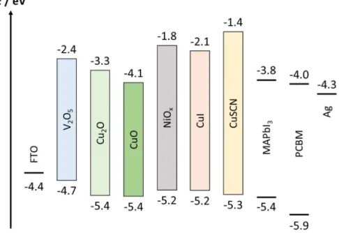
Dopant-Free Organic and Inorganic Hole Transport Materials
for Perovskite Solar Cells
(ペロブスカイト太陽電池のための添加剤フリー有機・無機正孔輸送材料)
全文
(ペロブスカイト太陽電池のための添加剤フリー有機・無機正孔輸送材料)
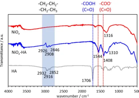
図

関連したドキュメント
Size Inset Hole P.C.D... Hub
Keywords: generalized Fokker – Planck; deterministic method; radiotherapy; particle transport; Boltzmann equation; Monte Carlo.. AMS Subject Classification: 35Q20; 35Q84; 65C05;
Also, a complex variable method have been applied to deduce exact expressions for Gaursat functions for the first and second fundamental problems of an infinite plate weakened by a
The (GA) performed just the random search ((GA)’s initial population giving the best solution), but even in this case it generated satisfactory results (the gap between the
In this paper, we extend the results of [14, 20] to general minimization-based noise level- free parameter choice rules and general spectral filter-based regularization operators..
Step 2: Reconstruction of the signal from the derived trace data by deconvolution (ill-posed)...
Based on sequential numerical results [28], Klawonn and Pavarino showed that the number of GMRES [39] iterations for the two-level additive Schwarz methods for symmetric
Motivated by ongoing work on related monoids associated to Coxeter systems, and building on well-known results in the semi-group community (such as the description of the simple