Applied Physics Express
Two-color surface-emitting lasers using a semiconductor coupled
multilayer cavity
Takahiro Kitada∗, Hiroto Ota, Xiangmeng Lu, Naoto Kumagai†, and Toshiro Isu
Graduate School of Science and Technology, Tokushima University, Tokushima 770-8506, Japan
Two-color surface-emitting lasers were demonstrated, employing a GaAs/AlGaAs coupled multilayer cav-ity composed of two cavcav-ity layers and three distributed Bragg reflector (DBR) multilayers. InGaAs multiple quantum wells (MQWs) with two different well widths were introduced only in the upper cavity, sandwiched between p-type and n-type DBRs. This current-injection type device exhibited two-color lasing in the near-infrared region under room temperature pulsed conditions. This two-color lasing was obtained when the lower cavity had an optimal thickness relative to the upper cavity thickness and the MQW emission proper-ties.
Terahertz light sources have been extensively investigated because of their wide range of potential applications, including wireless communications, spectroscopy, and imaging.1, 2)
Recent advances in femtosecond laser technology have it made possible to generate ultrashort terahertz pulses covering an extremely broad bandwidth.3–5)Several semiconductor-based
de-vices, such as quantum cascade lasers (QCLs),6–8)resonant tunneling diodes (RTDs),9, 10)and
photomixers11, 12)have also been studied and developed for use as continuous wave (cw)
tera-hertz emitters. Teratera-hertz sources based on intracavity difference-frequency generation (DFG) in dual wavelength mid-infrared QCLs have also been recently reported.13, 14)However, there are still challenges associated with each of these devices. As an example, the emission power of RTDs becomes insufficient when the devices are operated at higher frequencies. In addi-tion, although significant progress has been made with regard to terahertz QCLs, near-room temperature operation has not been demonstrated.
Optical microcavities are good candidates for nonlinear optical devices because an ex-tremely strong electric field is realized in a cavity layer sandwiched between two distributed Bragg reflector (DBR) multilayers. In addition, efficient wavelength conversion is possible in a GaAs-based multilayer cavity when the structure is grown on a non-(001) substrate, tak-ing advantage of the second-order nonlinearity of zincblende-type semiconductors.15)In fact,
∗E-mail: [email protected]
blue vertical cavity surface emitting lasers (VCSELs) utilizing the second-harmonic genera-tion (SHG) on (113)B and (114)A GaAs substrates have been reported.16)Recently, our own
group has proposed a GaAs/AlAs coupled multilayer cavity structure for use in novel ter-ahertz emitting devices.17) This structure consists of two equivalent cavity layers and three DBR multilayers. Such devices exhibit two cavity modes in the center of the high reflection band because a degenerate cavity mode is split into two different modes as a result of coupling of the cavity layers. It should be noted that this design allows the mode frequency difference to be precisely defined within the terahertz region according to the number of periods in the intermediate DBR. The electric field of each mode is greatly enhanced in both cavity layers, generating a strong frequency-mixed signal. Since the effective second-order nonlinear co-efficient is zero on a (001)-oriented GaAs substrate due to crystal symmetry,15) a non-(001)
substrate is essential for crystal growth. We have previously obtained a strong sum-frequency generation (SFG) signal from a GaAs/AlAs coupled multilayer cavity grown on a (113)B GaAs substrate when the two modes were simultaneously excited by 100 fs laser pulses.18–20) The peak intensity of the SFG signal was more than 400 times greater than that of the SHG from the (113)B GaAs bulk substrate. DFG signals from the (113)B coupled cavity samples were also demonstrated at room temperature by time-resolved waveform measurements using 100 fs laser pulses and a photoconductive antenna.21–23)In addition, we found that controlling
the nonlinear polarization via the face-to-face bonding of two epitaxial wafers is an effective means of obtaining a large terahertz DFG signal from two modes.24, 25)
From the viewpoint of practical device applications, the two modes should be generated inside the structure by current injection, since this enables terahertz emission through DFG without the requirement for external light sources. It should be noted that Carlin et al. al-ready demonstrated dual wavelength lasing in two-section vertical-cavity surface-emitting lasers (VCSELs) by current injection at room temperature.26, 27) In the two-section VCSEL, both cavities had gain regions consisting of InGaAs multiple quantum wells (MQWs), and they also intentionally introduced an asymmetry in the two cavity length to stabilize dual wavelength laser emission. However, the use of asymmetric two cavities is quite unsuitable for DFG of two modes through the second-order nonlinear response inside the structure be-cause the field overlap between two modes is largely reduced owing to the weak coupling of two cavities. In the current study, we have demonstrated current-injection two-color lasing
from the strongly coupled two-cavity system based on a GaAs/AlGaAs multilayer structure
that contains InGaAs MQWs with two different well widths solely in the upper cavity layer.
of the coupled multilayer cavity with self-assembled InAs quantum dots (QDs),28–31) and we
have recently found that significant optical loss results from the bonding interface when this
interface is located at an anti-node in the electric field distribution of the mode.31)In order to
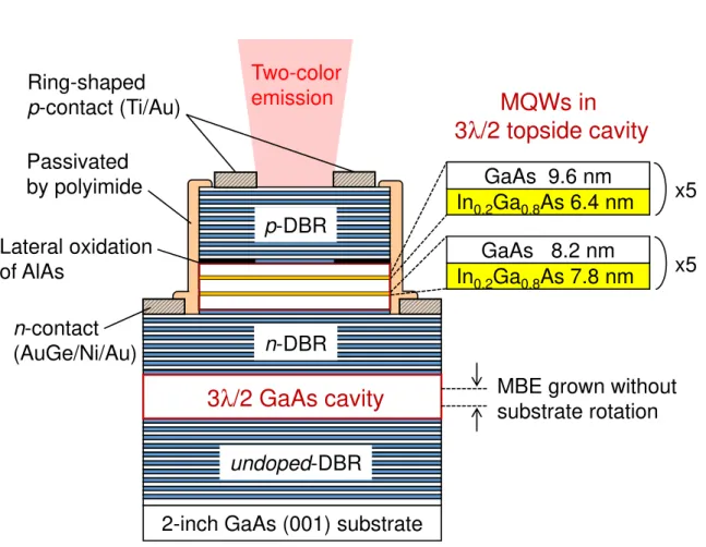
understand the intrinsic characteristics of two-color lasing in the coupled multilayer cavity, the entire structure employed in this study was prepared by solid-source molecular beam epitaxy on a single (001) GaAs wafer. Figure 1 shows a schematic of the two-color surface-emitting laser fabricated in this study on the 2 inch diameter (001) undoped-GaAs substrate. Two types of five-period In0.2Ga0.8As/GaAs MQWs, having well widths of either 6.4 or 7.8
nm, were introduced. These were situated solely in the upper 1.5 wavelength-thick (3λ/2) GaAs cavity, which was sandwiched between p-type and n-type GaAs/Al0.9Ga0.1As DBRs
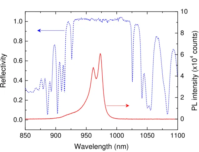
for current injection. The periods of the top, middle and bottom DBRs were 26, 12.5, and 30, respectively. Each MQW was placed at a position where a strong electric field was present for both modes. Be and Si were used as p-type and n-type dopants, respectively, and a 20 nm-thick, compositionally graded digital alloy layer was inserted in each GaAs/Al0.9Ga0.1As interface to reduce the electrical series resistance. It should be noted that a portion of the lower 3λ/2 GaAs cavity was grown without applying substrate rotation so that this lower cavity had a thickness distribution across the wafer. The nominal thickness of each layer was set to a specific value at which the cavity modes would coincide with the MQW emission peaks. Figure 2 presents the room temperature photoluminescence (PL) spectrum of a reference MQW sample that had the same layer structure as used in the upper cavity of the device. The optical reflection spectrum acquired at the center of the coupled cavity wafer is also plotted in Fig. 2. Two PL peaks due to the MQWs with two different well widths are clearly evident at 962 and 973 nm. The midpoint of these two values is slightly shorter than the central wavelength of the high-reflection band realized in the coupled cavity wafer.
The current-injection surface-emitting devices were fabricated by depositing a ring-shaped Ti/Au (5 nm/100 nm) electrode onto a p-type DBR surface, after which a circular mesa with a diameter of 100µm was formed via a three-step wet etching process. This con-sisted of (1) etching the p-type DBR using a phosphoric acid solution, (2) selective etching of the upper cavity using a citric acid solution, and (3) selective etching of the upper n-AlGaAs layer of the intermediate DBR using a more dilute phosphoric acid solution. In order to real-ize the current confinement structure, a thin AlAs layer inserted just above the upper cavity was selectively oxidized from the sidewall. This lateral oxidation of the AlAs was accom-plished by annealing at 480◦C under a humid atmosphere, supplied by bubbling nitrogen gas through deionized water maintained at 80◦C. An n-type electrode was subsequently formed
by depositing AuGe/Ni/Au (50 nm/12.5 nm/50 nm) onto the exposed n-type DBR surface, followed by rapid thermal annealing at 430◦C under nitrogen. Finally, a polyimide film coat-ing was applied as a passivation layer.
The devices were operated at room temperature using a pulsed current source with a pulse duration of 1 µs and a duty cycle of 0.1%. The light emitted from the optical window of each device was detected using a spectrometer equipped with a thermoelectrically cooled Si charge-coupled device array. The injection current was varied from 10 to 70 mA. Two sharp emission peaks due to the cavity modes were clearly observed in all spectra. Figure 3 plots the intensities of the two emission peaks as functions of injection current for three different devices that were fabricated on a single epitaxial wafer. The emission spectra of each device acquired at the currents indicated by the arrows are also presented in this figure. In each device, the lower cavity had a slightly different thickness because of the intentional thickness distribution across the wafer. The thickness differences were roughly estimated by the frequency differences of the two cavity modes observed in the emission spectra and the wafer positions of the three devices. In the case of Fig. 3(a), the device had a relatively thin lower cavity, which was ∼2% and ∼5% thinner compared to the devices of Fig. 3(b) and 3(c), respectively, and the long-wavelength mode exhibits threshold behavior at a current of approximately 30 mA, which is not observed for the short-wavelength mode. Conversely, in Fig. 3(c), the device had a rather thick lower cavity and a threshold is only observed for the short-wavelength mode. These single-color lasing behaviors can be explained by considering the electric field distribution of each mode when two cavities with different optical thick-nesses are coupled. If the optical thickness of the lower cavity is less than that of the upper cavity, the electric fields of the short- and long-wavelength modes will tend to localize in the lower and upper cavities, respectively.30)In this case, the long-wavelength mode will have a much stronger electric field in the MQW region compared to the short-wavelength mode, so that the stimulated emission will be more likely to occur in the long-wavelength mode, as observed in Fig. 3(a). For similar reasons, the short-wavelength mode will be associated with stimulated emission when the lower cavity is thicker than the upper cavity, as in Fig. 3(c). In contrast to these two results, both modes show a threshold at approximately 45 mA in Fig. 3(b), in which case the lower cavity had a thickness between those of the other two devices. This result indicates that the lower cavity thickness is an important parameter with regard to achieving two-color lasing of the device.
Here we consider the necessary conditions for the two-color lasing. Both cavities should have exactly the same optical thickness, so that the two modes have identical electric field
intensities in the MQW region. In addition, the MQW emission properties of the two mode wavelengths should also be exactly the same so as to obtain an identical optical gain for each mode. Although the PL intensities of the bare MQWs at the two mode wavelengths of 971.4 and 980.9 nm did not closely match one another (Fig. 2), we did observe two-color lasing at a specific lower cavity thickness. Therefore, differences between the MQW emission proper-ties of the two mode wavelengths can be compensated for by selecting the appropriate lower cavity thickness. It may also be possible to allow for a slight difference in thickness between the two cavities by tuning the operational temperature that governs the spectral position of the MQW emission. This would be very practical with regard to actual device operation. We also note the peculiar behaviors of the two modes observed in Fig. 3(b). As the current was increased, the lasing action initially occurred in the long-wavelength mode, immediately after which the short-wavelength mode began to oscillate. The intensity of the short-wavelength mode increased with further current increases while the long-wavelength mode showed an al-most constant intensity. However, at a current of 52 mA, the intensity of the long-wavelength mode suddenly jumped to a much higher value, after which it increased with the current. These phenomena strongly suggest that optical gains in the two modes are correlated with one another, as the result of the nature of the electronic states in the two-dimensional MQW system. Here we have to consider the simultaneity of two-color lasing in our device. As in Fig 3(b), the mode competition seemed to cause the anomalous behavior of the long-wavelength mode emission in the current region of 40–55 mA. On the other hand, emission intensities of both modes monotonically increased with the current in the high injection region above 60 mA, where sufficiently high optical gains should be provided, indicating the stable two-color lasing. Therefore, simultaneous two-color lasing was very likely to be realized at least in the high injection region. In all the measurements, intensity and polarization instabilities of the two mode emission were not observed at any pulsed current. For the actual terahertz emitting device, it should be considered that each mode emission is polarized in the specific crystal axis so that the strong DFG is enabled.
In conclusion, this work demonstrated two-color surface-emitting lasers based on a GaAs/AlGaAs coupled multilayer cavity that consisted of two cavity layers and three DBR multilayers. Two types of five-period InGaAs/GaAs MQWs were introduced exclusively in the upper cavity, sandwiched between p-type and n-type DBRs. A number of devices were fabricated on a single epitaxial wafer in which the lower cavity had an intentionally induced lateral thickness variation, and the resulting emission characteristics in the near-infrared re-gion were assessed at room temperature under pulsed conditions. Two-color lasing of the
device was observed when the lower cavity had an appropriate thickness as defined by the upper cavity thickness and the MQW emission properties. The present study therefore de-termined that useful terahertz emitting devices can be obtained by ensuring that the coupled cavity structure has second-order nonlinearity suitable for DFG of the two modes, which can be accomplished by face-to-face bonding of (001) and (113)B epitaxial wafers designed to eliminate optical loss at the bonding interface.
Acknowledgments
This work was partly supported by the Strategic Information and Communication R&D Pro-motion Programme (SCOPE) of the Ministry of Internal Affairs and Communications, Japan, and also by a Grant-in-Aid for Scientific Research (B) (No. 16H04351) from the Japan Soci-ety for the Promotion of Science (JSPS).
n
-contact
(AuGe/Ni/Au)
2-inch GaAs (001) substrate
p
-DBR
n
-DBR
undoped
-DBR
Ring-shaped
p
-contact (Ti/Au)
Passivated
by polyimide
Lateral oxidation
of AlAs
In
x5
0.2Ga
0.8As 7.8 nm
GaAs 8.2 nm
In
0.2Ga
0.8As 6.4 nm
GaAs 9.6 nm
x5
3
λ
/2 GaAs cavity
MQWs in
3
λ
/2 topside cavity
Two-color
emission
MBE grown without
substrate rotation
Fig. 1. Schematic of the two-color surface-emitting laser incorporating a GaAs-based coupled multilayer cavity.
850
900
950
1000
1050
1100
0.0
0.2
0.4
0.6
0.8
1.0
R
e
fl
e
c
ti
v
it
y
Wavelength (nm)
0
2
4
6
8
10
P
L
i
n
te
n
s
it
y
(
x
1
0
4c
o
u
n
ts
)
Fig. 2. Room temperature PL and reflection spectra. PL was measured for a reference MQW sample with the same layer structure as used in the upper cavity.
0 10 20 30 40 50 60 70 ÝÜÞ ÝÜß ÝÜà ÝÜá ÝÜâ 0 10 20 30 40 50 60 70 ÝÜÞ ÝÜß ÝÜà ÝÜá ÝÜâ 0 10 20 30 40 50 60 70 ÝÜÞ ÝÜß ÝÜà ÝÜá ÝÜâ 940 960 980 1000 940 960 980 1000 940 960 980 1000 S L P e a k i n te n s it y ( lo g -c o u n ts ) Current (mA)
(a)
(b)
S L P e a k i n te n s it y ( lo g -c o u n ts ) Current (mA)(c)
S L P e a k i n te n s it y ( lo g -c o u n ts ) Current (mA) 31 mA L S Wavelength (nm) 45 mA L S Wavelength (nm) 31 mA L S Wavelength (nm)Fig. 3. Peak emission intensities of the two modes plotted as functions of injection current for three different devices. The lower cavity thickness was slightly increased going from (a) to (c) due to the intentional thickness distribution across the wafer. Each right-hand panel shows the lasing spectrum of the corresponding device measured at the current indicated by the arrow in the left-hand plot.
References
1) M. Tonouchi, Nat. Photonics 1, 97 (2007).
2) W. L. Chan, J. Deibel, and D. M. Mittleman, Rep. Prog. Phys. 70, 1325 (2007). 3) D. H. Auston, K. P. Cheung, and P. R. Smith, Appl. Phys. Lett. 45, 284 (1984). 4) P. Y. Han and X.-C. Zhang, Appl. Phys. Lett. 73, 3049 (1998).
5) M. Nagai, K. Tanaka, H. Ohtake, T. Bessho, T. Sugiura, T. Hirosumi, and M. Yoshida, Appl. Phys. Lett. 85, 3974 (2004).
6) R. K¨ohler, A. Tredicucci, F. Beltram, H. E. Beere, E. H. Linfield, A. G. Davies, D. A. Ritchie, R. C. Iotti, and F. Rossi, Nature 417, 156 (2002).
7) B. S. Williams, Nat. Photonics 1, 517 (2007).
8) M. A. Belkin, J. A. Fan, S. Hormoz, F. Capasso, S. P. Khanna, M. Lachab, A. G. Davies, and E. H. Linfield, Opt. Express 16, 3242 (2008).
9) M. Asada, S. Suzuki, and N. Kishimoto, Jpn. J. Appl. Phys. 47, 4375, (2008).
10) S. Suzuki, M. Asada, A. Teranishi, H. Sugiyama, and H. Yokoyama, Appl. Phys. Lett. 97, 242102 (2010).
11) S. Matsuura, M. Tani, and K. Sakai, Appl. Phys. Lett. 70, 559 (1997).
12) H. Ito, F. Nakajima, T. Furuta, K. Yoshino, and T. Ishibashi, Electron. Lett. 39, 1828, (2003).
13) K. Vijayraghavan, Y. Jiang, M. Jang, A. Jiang, K. Choutagunta, A. Vizbaras, F.
Demmerle, G. Boehm, M. C. Amann, and M. A. Belkin, Nat. Commun. 4, 2021 (2013). 14) K. Fujita, M. Hitaka, A. Ito, T. Edamura, M. Yamanishi, S. Jung, and M. A. Belkin,
Appl. Phys. Lett. 106, 251104 (2015).
15) N. Yamada, Y. Ichimura, S. Nakagawa, Y. Kaneko, T. Takeuchi, and N. Mikoshiba, Jpn. J. Appl. Phys. 35, 2659 (1996).
16) Y. Kaneko, S. Nakagawa, Y. Ichimura, and N. Yamda, J. Appl. Phys. 87, 1597 (2000). 17) T. Kitada, F. Tanaka, T. Takahashi, K. Morita, and T. Isu, Appl. Phys. Lett. 95, 111106
(2009).
18) F. Tanaka, T. Takahashi, K. Morita, T. Kitada, and T. Isu, Jpn. J. Appl. Phys. 49, 04DG01 (2010).
19) K. Morita, F. Tanaka, T. Takahashi, T. Kitada, and T. Isu, Appl. Phys. Express 3, 072801 (2010).
20) F. Tanaka, T. Takimoto, K. Morita, T. Kitada, and T. Isu, Jpn. J. Appl. Phys. 50, 04DG03 (2011).
21) K. Morita, S. Katoh, T. Takimoto, F. Tanaka, Y. Nakagawa, S. Saito, T. Kitada, and T. Isu, Appl. Phys. Express 4, 102102 (2011).
22) S. Katoh, T. Takimoto, Y. Nakagawa, K. Morita, T. Kitada, and T. Isu, Jpn. J. Appl. Phys. 51, 04DG05 (2012).
23) T. Kitada, S. Katoh, T. Takimoto, Y. Nakagawa, K. Morita, and T. Isu, IEEE Photonics J. 5, 6500308 (2013).
24) T. Kitada, F. Tanaka, T. Takahashi, K. Morita, and T. Isu, Proc. SPIE 7937, 79371H (2011).
25) T. Kitada, S. Katoh, T. Takimoto, Y. Nakagawa, K. Morita, and T. Isu, Appl. Phys. Lett. 102, 251118 (2013).
26) J. F. Carlin, R. P. Stanley, P. Pellandini, U. Oesterle, and M. Ilegems, Appl. Phys. Lett. 75, 908 (1999).
27) M. Brunner, K. Gulden, R. H¨ovel, M. Moser, J. F. Carlin, R. P. Stanley, and M. Ilegems, IEEE Photonics Technol. Lett. 12, 1316 (2000).
28) T. Kitada, C. Harayama, K. Morita, and T. Isu, Phys. Status Solidi C 10, 1434 (2013). 29) C. Harayama, S. Katoh, Y. Nakagawa, K. Morita, T. Kitada, and T. Isu, Jpn. J. Appl.
Phys. 53, 04EG11 (2014).
30) C. Harayama, S. Katoh, Y. Nakagawa, X. M. Lu, N. Kumagai, T. Kitada, and T. Isu, Jpn. J. Appl. Phys. 54, 04DG10 (2015).
31) H. Ota, X. M. Lu, N. Kumagai, T. Kitada, and T. Isu, Jpn. J. Appl. Phys. 55, 04EH09 (2016).