九州大学学術情報リポジトリ
Kyushu University Institutional Repository
High Direct Modulation Speed with Space Mode Selectivity by Using Active Multimode
Interferometer Laser Diode
洪, 秉宙
http://hdl.handle.net/2324/2236274
出版情報:九州大学, 2018, 博士(学術), 課程博士 バージョン:
権利関係:
High Direct Modulation Speed with Space Mode Selectivity by Using Active
Multimode Interferometer Laser Diode
Department of Applied Science for Electronics and Materials Interdisciplinary Graduate School of Engineering Sciences
Kyushu University Japan
Bingzhou Hong
Contents
Abstract 1
Chapter 1 Introduction 1.1 Optical link technologies for supercomputer system and next generation and IoT device 3
1.2 Mode Manipulating Optical Devices: State of the Art 10
1.3 High Speed Semiconductor Lasers: State of the Art 16
1.4 Outline of This Thesis 22
References 23
Chapter 2 Mode Selective Light Source Based on Active-Multimode Interferometer Laser Diode 2.1 Introductory Overview 36
2.2 Theory of Multimode Interferometer 37
2.3 Design of mode selective light source 44
2.4 Mode Selective Light Source Based on Active-Multimode Interferometer Laser Diode 50 References 57
Chapter 3 High Direct Modulation Bandwidth Active-Multimode Interferometer Laser Diode 3.1 Introductory overview 61
3.2 Modified small signal response taking PPR into consideration 63
3.3 Scheme of bandwidth enhancement method targeting more than 100 GHz bandwidth 70
References 84
Chapter 4 Mode Selective Light Source with over 40 GHz Direct Modulation Bandwidth 4.1 Introductory overview 87
4.2 Scope, design and fabrication of high speed mode selective active-MMI LD 88
4.3 Mode selective output characteristics of the device 97
4.4 Over 40 GHz bandwidth mode selective light source 100
References 107
Chapter 5 Conclusions and Future Work 5.1 Conclusions 108
5.2 Future Works 110
References 111
Abstract
This thesis discussed the research on high speed mode selective light source. With the huge development of mobile technology, and super computer technology, the inner connection link bandwidth requirements have reached new level. In the near future, it is predicted that the 1 Tb/s level speed is necessary for such links. In general, only optical communication links can provide such huge bandwidth. Thus, the high speed direct modulated laser diodes that can be used in such optical links is the best candidate to be integrated within compact size mobile devices. Although wavelength length division (WDM) technology could be used to enhance the capacity, the relative complex WDM system is not suitable for integrated device system.
Especially when considering the fact that mobile devices are extremely sensitive to the power consumption, a single chip that can operate on Tb/s level with low energy consumption is desired. On the other hand, similar to wavelength, optical mode has also been researched intensively to carry information. By utilizing spatial mode division multiplexing (SDM) technology, the transmission capacity is also largely enhanced. In such case, SDM can also be used for such inner connection optical links. In terms of SDM technology, considering single mode carries 100 Gb/s level signal, integration of 10 modes can bring 1 Tb/s level in total. In this thesis, the high speed mode selective light source is discussed.
The first issue is to design the mode selective light source. As the first trial, two lateral mode selective light source has been demonstrated. The core principle to design the mode selectivity is to separate propagation path within the device for each single mode. After separation, the current injection electrodes into each mode section are also separated electrically. By setting so, the current injected into each mode propagation path is controlled.
(active-MMI LD) has an MMI section at central part of the device, multiple optical modes are introduced and separated inside the device. As a result, active-MMI LD is the best candidates for mode selective light source.
Another issue is to achieve the high direct modulation bandwidth on laser diode.
Traditional laser diode bandwidth is limited by the carrier photon resonance, which is the intrinsic physical bottleneck. On the other hand, photon photon resonance phenomenon (PPR) has been researched to extend the modulation bandwidth. Although PPR largely extend the bandwidth to more than 60 GHz on two section DBR lasers, the damping at high frequency still limits the furthermore bandwidth enhancement. To solve such problem and to extend the bandwidth to extremely high frequency range such as more than 100 GHz level, multiple PPRs ideals are proposed. By setting multiple PPRs that are placed not far from each other, the damping between each PPR can be compensated. Actually, ideal of multiple PPR is able to extend the modulation bandwidth to infinite level in principle. To achieve multiple PPRs, the basic requirement is to introduce multiple oscillating cavities inside the laser diodes. The active-MMI LD is able to integrate multiple access waveguides that acts as oscillating cavities, which exactly satisfied such requirements. Furthermore, by utilizing high-mesa waveguide, the MMI edge forms an inner reflection mirror, which further introduces much more inner reflection mirrors. Based on the ideal described above, 1 by 3 active-MMI LD with 34 GHz direct modulation bandwidth is fabricated. With the combination of the two ideals described above, mode selectivity and high speed scheme are combined within single device. As a result, a 1 by 3 active MMI LD with selective output mode are demonstrated. Because of the existence of multiple PPRs, over 40 GHz bandwidth for each single mode has been confirmed. Such high speed mode selective light source is the proof of design and fabricate a single laser chip with over 1 Tb/s level capacity.
Chapter 1 Introduction
1.1 Optical link technologies for supercomputer system and next generation and IoT device
Modern society has tremendous need on computation, for instance scientific research, bio- medical diagnostics, national securities and stock market simulation [1]. All such needs are now highly relied on the super computer systems that can process huge amount of data fast and efficiently. The super computer system itself is consist of large number of micro-processor cores that are connected with each other. Most of the case, the micro-processors and memory directly linked with each other. In general, higher inner connection bandwidth/speed results in higher computation speed as well as efficiency. The word top supercomputers have experienced quick inner connection bandwidth improvement since year 2000 [2]. The super computer systems have been using optical links for data transmission in mainly because of its high bandwidth and energy efficiency when compared with electrical links. Table 1.1 shows such inner connection link improvement of top super computers in the word [3-13].
Table 1.1
Inner link bandwidth improvement of supercomputer
Name Year Node-to-node bandwidth [Gb/s]
BlueGene/L [14] 2002 0.4
Gray Seastar [16,17] 2004 1.2
Infiniband DDR-4x 2005 1.9
BlueGene/P [19] 2008 2.8
Infiniband QDR-4x 2008 2.8
Tofu [24] 2010 4.76
Gray Gemini [25] 2010 3.6
BlueGene/Q [28] 2012 1.75
Gray Aries [30] 2012 8-10
TH Express-2 [31] 2013 11.8
Tofu 2 [32] 2014 45.82
As can be seen in the chart, the inner connection speed between micro-processor cores has been increasing dramatically. It is predicted that, with the emerging technologies and products (multimode transmission, silicon photonics and other transceiver technologies), at least 100 Gb/s bandwidth (speed) is necessary for next few years upcoming computer systems [2]. The next subsections overview the current and to-be-deployed optical interconnect technology that is used/to be used for supercomputers/High Performance Computers (HPCs).
Based on the review, technical challenges as well as solutions for next generation supercomputer/HPCs and 5G/IoT devices are discussed.
1.1.1 Multimode transceiver based links
The Vertical Cavity Surface Emitting Lasers (VCSELs) and few-mode/multi-mode optical fibers is the foundation of most optical links in supercomputers nowadays [20]. Such system is based on single channel per fiber format and direct modulation laser (DML) technology is applied [21]. Standardization organizations such as IEEE has recommended the transceivers receiving electrical signal at 10 14, 28 Gb/s on one to ten lanes that is coupled into its separate fiber. To further explore the supercomputer performance, transceiver with 56 Gb/s for supercomputer will be released into commercial market very soon. The standards for electrical signaling at 112 Gb/s are in preparation since 2015 [22]. Error free 56 Gb/s non- return-to zero (NRZ) modulation based VCSEL links have been shown capable of supporting extreme bitrates [23]. The near future supercomputer system is only about to use multiple
One fatal issue of the multi-fiber system is the fiber cable management and cable cost.
Moreover, higher loss is introduced in such system which necessitate the deployment of amplifiers and other loss-compensation structure [25]. Multiple wavelength (WDM) links has been proposed to solve such issue [26]. With the high speed signaling beyond 50 Gb/s on VCSEL as well as coarse WDM technology based on several fiber might resolve the bottleneck of speed limitation [27]. One ambitious target is to achieve up to 1Tb/s/channel level based on such technology.
1.1.2 Silicon photonics based transceiver based links
As an emerging technology of recent several decades, the Silicon Photonics (SiP) technology has been attractive, mostly because of abundance of Silicon material as well as the superior electrical property [28]. The silicon material based deices can be manipulate with extremely high accuracy. Furthermore, unlike other materials, SiP based devices has higher refractive index contrast, which brings the possibility of integrating devices at micro-meter order scale [29]. Silicon-based high speed modulator uses the so called free-carrier effect [30]
for modulation. It is easy to achieve 10 Gb/s level and beyond [31] on such devices. The array of such modulators can achieve more than 100 Gb/s [32]. Mach-Zehnder based silicon modulators, which are less sensitive to thermal fluctuation , are also commonly used for similar applications [33]. As silicon is not the direct bandgap material [34], such material based device is extremely poor light emitter. Thus, unlike direct modulated lasers (DML) such as VCSELs or DFB lasers, an external laser or light source is inevitable for such system when modulating.
Normally III-V semiconductors are used for such light source [35].
Wavelength division multiplexing (WDM) technology can provide promising inner connection bandwidths that satisfy the requirements of super computer in the near future [36].
per line for super computer system [37]. More recently, maximum aggregation of more than 2.1 Tb/s at 45 GHz sampling rate was proposed for link level of SiP based interconnectors [38].
Besides that, a 1.56 Tb/s inner connection link has also been proposed [39]. Although all the proposal or analysis are within laboratory level, for practical links 1Tb/s is an acceptable level.
However, all these links are based on single mode fiber, which brings a serious problem of coupling issue, mainly because of the mismatch between SiP based waveguide core width and the fiber diameter. Such issue is quite easy in the case of VCSELs based links, simply because of VCSELs’ wide aperture, and it is easier to couple light from VCSELs to multimode fibers.
1.1.3 Toward next generation optical links for supercomputer and IoT technology
For next generation supercomputer system, the most critical issue lies on how to explore computational density. Moore’s Law continues improve the transistor density and consequent the micro-processor performance density. The connections for standard chip, however, does not benefit from Moore’s Law thus the connection density is not increasing dramatically. To keep up with the tremendously increased information capacity between processors and memories, one solution is to enhance the connection bandwidth between memories. Actually, bandwidth limitation between memories and/or processors is now particularly becoming the fundamental limitation, especially the conventional electrical wires [40, 41]. The optically connect memory (OCM) has been proposed as recent micro-meter scale SiP devices have been keeping in progress [42-44].
Based on the review above, it is quite clear that in order to satisfy the requirements for next generation supercomputers, the main issue resides on how to send data that is generated from micro-processors to another. Although VCSELs based links or SiP based links both can satisfy sort part of the requirements, it is much better to combine the advantages of both
The main problem is the average cost reduction of VCSELs based links [46]. Furthermore, thanks to the relative wide aperture of VSCESLs, it is not a tough work for coupling. WDM technology on SiP based devices of course can provide the bandwidth that is needed for supercomputer in near future, and Tb/s level or even much more is quite feasible for such links [47]. The annoying issue is to cost of light source that emits different wavelength individually for WDM application [48]. Thus, there are strong motivations to co-integrate the advantages of the above technics both.
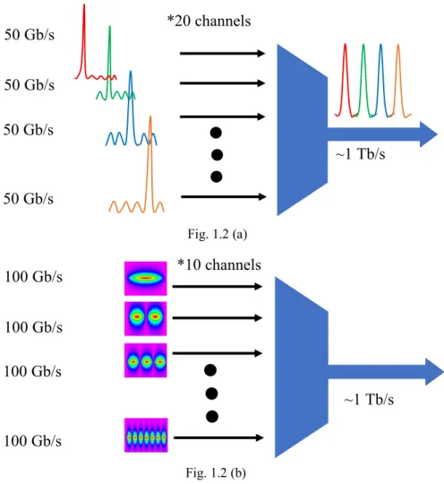
To apply both technologies, we have proposed to use spatial mode multiplexing (SDM) based optical links for supercomputers as well as IoT devices, which combines high speed direct modulated light source as well as SiP based waveguides. When considering how micro- processor cores communicate with the memory, the connection between processors and memory needs precise arrangement. Figure 1.1 shows such idea. Data(signal) from processor are send by high speed mode selective light source using direct modulation and transmitted to memory through optical waveguide. Here, we propose to apply the spatial mode multiplexing technology. Although WDM technology is used for conventional inter connecter links, the spatial mode of light has similar function just like wavelength, simply because it is also an individual freedom of light [49].
Considering that single spatial mode carries over 100 Gb/s signal, by multiplexing more than 10 modes one can achieve 1 Tb/s level. The problems became quite simple—the main issue is to achieve a single device that includes multiple individual spatial modes, and for each
Figure 1.1 Cross section view of High-Speed Mode Selective Light Source based inter connection
Processor Memory
Memory
High Speed Mode Selective Light Source
Optical Waveguide Optical
Waveguide
(b) illustrate and compare such structures. The link of Fig. 1.2 (a) is based on WDM technology while the Fig. 1.2 (b) is based on SDM technology. Considering that to integrate laser emitting different light source, the several controller/laser designs are necessary, resulting in higher cost.
We propose the SDM based links, which utilize single light source that emitting different planar modes while each mode could be modulated directly at extremely high speed. Thus, based on the structure we proposed, the laser design can be done for only once. Hence the cost could be cut down. Furthermore, considering that all the laser chips are quite tinny and have small footprint, the integration of such device on small electrical devices such smart phones or some other potable device is quite valid. Such devices are quite fundamental equipment for
50 Gb/s
50 Gb/s 50 Gb/s
50 Gb/s
*20 channels
~1 Tb/s
*10 channels 100 Gb/s
100 Gb/s 100 Gb/s
100 Gb/s
~1 Tb/s
Fig. 1.2 (a)
Fig. 1.2 (b)
Fig. 1.2 Two technologies be used for supercomputer links. (a) WDM based link illustration (b) SDM based link illustration
Targeting light source for such era, the laser diode we explore must integrate the following characteristics: 1. Mode selectivity and 2. High direct modulation speed. Mode selectivity itself is strongly related to mode manipulating principles, thus it is of great necessity to overview the history and principle of mode manipulating technology. High speed modulation, on the other hand, is another main subject of our work. Its history will also be reviewed.
1.2 Mode Manipulating Optical Devices: State of the Art
Although the optical communication transmission capacity has increased tremendously, recent internet data explosion has been accelerating [50]. The transmission capacity of single optical fiber has reached its bottleneck simple because of the inner physical limitation of optical fiber [51]. Spatial distribution of light is one of the freedoms that can carry information compatible with time, frequency (or wavelength) or polarization. Thus, in order to enhance the transmission capacity spatial mode division multiplexing (SDM or MDM) has been proposed and researched intensively [52-63]. The SDM related optical devices are mainly mode converters, mode multiplexers/de-multiplexers, or some other mode related devices [46-60].
Although such devices are designed for transmission systems while not specifically for system- on-chip, it is necessary to review the mode manipulating optical devices for a thorough understanding of the inner principle.
Mode conversion has been researched quite a lot for MDM transmission with integrated optic components, such as phase plates and spatial light modulators [63, 64]. For instance, a
SMF port 0
SMF port 1
SMF port 2 Phase Plates
Beam Splitters f1 f2
Mirror Lenses
Fig. 1.3. Schematic view of 6-mode FMF mode multiplexer
1.3 shows the schematic view of such MUX. Although such setup is used for MUX, it can excite multiple modes simultaneously from basic fundamental mode, which plays the role of mode converter. The beam splitters are used for exciting higher order modes. By adjusting the incident light power from SMF 0, 1, and 2 as well as the phase plates angle, the output modes are somewhat the liner combination of LP11 spatial and polarization modes.
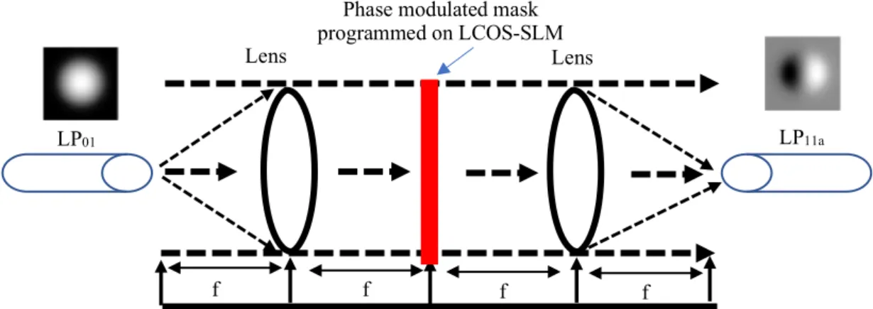
Light modulator based mode converter is another choice [64]. Figure 1.4 shows such structure. A liquid crystal on silicon (LCOS) spatial light modulator (SLM) with two lenses consist of a phase modulator to change the phase of the transverse distribution of the optical field [64]. The original LP01 (phase is 0) mode is converted into LP01a (phase is 0/180, left and right) or LP01b (phase is 0/180, up and down) based on the adjustment of phase modulation in the LCOS-SLM section. Similar to the 6-modes converter, the LCOS-SLM also has a distinguished function for mode multiplexing.
Phase modulated mask programmed on LCOS-SLM
Lens Lens
f f f f
LP01 LP11a
Fig. 1.4. Scheme of mode conversion using SLM phase mask on the Fourier plane of a 4f configuration
OFT OFT OFT OFT OFT OFT
Input mode Output mode
Transverse intensity
Mode conversion utilizing a couple of planes is a normal solution for higher order mode generation [65]. Such ideal is quite similar as the lens based system. The spatial multiplexing fundamentally transforms a mode basis to another mode basis, and theoretically, for any desired spatial unitary transform between an input and output plane, a group of succession of transverse phase profiles which is separated optical Fourier transforms (OFT) will achieve the desired unitary transform [66]. In another word, an appropriate arrangement of the phase control plate, an arbitrary mode conversion is possible. A multi-plane light conversion system is shown in Fig. 1.5. Such plates/planes are also called spatial light modulators (SLMs). As shown in the figure, the input light is converted gradually through a group of Fourier transform
Fig. 1.6. Schematic view of mode converter from TE00 to TE01
plates. The phase of light is changed hence the intensity distribution profile is changed, and finally the mode pattern is converted. Such spatial light modulated setup is, actually, sort of too much complicated and not quite suitable for integration. Consequently, some other compact size mode converters are attracting attention nowadays.
The silicon photonics based mode converter have also been researched intensively [67- 80] simply because the compact size. The early compact mode converter between Zeroth-and First- order mode converter utilizing phase difference between two propagation brunch [68]
were fabricated on double trench structure. Such structure is shown in Fig. 1.6. The input TE00
mode is separated into two sub power peaks with equal power ratio. After a pi phase delay, the recombination light is reformed 1st order mode then. A multimode brunch series were used for Five-order mode converter [69]. The proposed structure shows the feasibility of converting arbitrary mode from TE00 to TE40 by changing the connection sequences of the brunches. Such configuration is shown in Fig. 1.7.
Actually, mode converter based on photonic lantern has been researched intensively because such structure offers low insertion loss, low mode dependent loss, scalability and compactness [70-72]. Figure 1.8 shows a typical photonic lantern structure that is used widely currently. More recently, photonic lantern 10 mode (20 vector modes) converter [70] was proposed and fabricated in 2017. Such photonic lantern utilized low index micro structured drilling preforms. Besides the conventional photonic lantern that convert certain modes into the others, the mode-selective photonic lantern has also been proposed and fabricated in 2014
Fig. 1.8. Photonic lantern spatial multiplexer structure
dissimilar optical fibers [72] rather than identical ones as in standard photonic lantern [73, 74].
One issue of photonic lantern mode converter is the necessary of an additional optical device to separate the degenerated modes for mode multiplexer, and the phase control device is needed for the multiplexer to excite the degenerated modes [75]. Although the mode selective photonic lantern does not need to separate the same mode group [76], multi-in-multi-out (MIMO) process is still inevitable.
Some other waveguide type mode multiplexers were also researched because they are suitable for the integration with other waveguide type optical devices such as optical wavelength filters and is quite compact when compared with other type multiplexers [77].
Fig. 1.9. Schematic view of 3 mode multiplexer based on stacked polymer waveguide
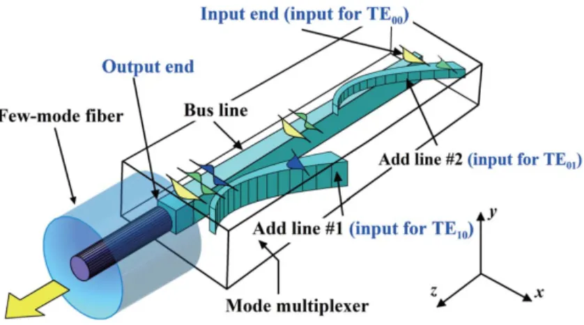
Yokohama National University has proposed and fabricated the stacked polymer waveguide type multiplexer for few mode fibers in 2015 [78]. Such structure is shown in Fig. 1.9. Three different input port was designed, and such device is directly coupled into a few mode fiber.
TE00, TE10, and TE01 modes can be excited from such device.
Hokkaido University and NTT has proposed and fabricated a planner light wave circuit for 6 mode multiplexing or demultiplexing. Such device is shown in Fig. 10. One interesting point is that such device is reversible. MUX/DEMUX has a pair of input/output port. LP01 mode up to LP02 mode (6 modes in total) is applicable on such device. Another mode converter based on optical mode switch was proposed in 2014 [79]. Such device shown in Fig. 1.11 is based on optical mode switch, and up to 4 modes (planer waveguide modes) could be supported and converted. It is kind of similar to the cascade structure in Fig. 1.5.
All the mode manipulating devices here are based on passive material, however, no active device that directly control the mode has been intensively studied yet. Thus, one of the aim of this work is to investigate the mechanism of introducing mode manipulating phenomenon into active devices.
Fig. 1.11. Schematic view of optical mode switch for 4 mode switching system
1.3 High Speed Semiconductor Lasers: State of the Art
1.3.1 literature review of research on Photon Photon Resonance
The high speed transmitters that are promising candidates for future data center use at 400 Gb/s – 800 Gb/s system has been intensively studied [81-83]. As the upcoming supercomputer will need data speed of Tb/s level, modulators with much better performance will be needed.
The electro-absorption modulators and Mach-Zehnder type modulators do have promising modulation speed, however, the footprint is the fatal problem for future integrated devices for small machines at extremely high speed [2]. Here we discuss the history of direct modulated lasers (DMLs) as its size is compact. More importantly, the energy efficiency of DML is much higher than that of external modulated lasers [84].
The direct modulation bandwidth (BW) of DMLs are intrinsically limited by the differential gain [85], thus the traditional DMLs BW has an intrinsic resonant frequency (Fr) when modulated. Lots of attempts have been done to extend the bandwidth by enhance the Fr frequency [86-90]. The damping of the S21 response at high frequency is fatal and only extend the Fr frequency is not enough when much higher BW is needed. In general, by introducing an external cavity beside the main lasing cavity will provide an optical feedback inside the laser.
Such feedback in fact forms an additional longitudinal mode that can enhance the modulation bandwidth [91-97]. Such phenomenon is called photon-photon resonance (PPR) and can actual extend the direct modulation bandwidth of the DML drastically. The principle behind will be discussed in chapter 3 in details for better understanding.
The history of research on PPR can be dated back to early 1980s, which was revealed by Roy Lang and Kohroh Kobayashi when studying external optical feedback effects on
related with the light feedback time. In general, the essential factor to introduce the PPR is the existence of external cavity or compound cavity (effective compound cavity) inside the lasers.
Because such cavities can introduce optical feedback that can induce an extra optical enhancement for longitudinal sideband. Later, some research specifically on modulation frequency response of laser diode in terms of PPR phenomenon has been done. Doctor Larry A. Coldren firstly investigated the modulation properties of coupled-cavity lasers in 1984 [99].
Ten years later, doctor Marcenac investigated the modulation bandwidth property in push-pull modulated DFB lasers in 1994 [100]. Since the year 1995, after some of the pioneering work of multi-cavity lasers, PPR phenomenon seems attracted people’s attention specifically because of its superior property of extend the direct modulation bandwidth on semiconductor lasers.
The explore of PPR applications has been intensively researched [86-90] experimentally, and Table 1.2 summarized the experimental research on PPR.
Table 1.2
Summary of experimental results on PPR research Institution Cavity
Structure
Bandwidth (GHz)
PPR Numbers
Year Publication
Tokyo Institution of
Technology
Transverse coupled VCSEL
29 Single 2013 Applied
Physics Letters Finisar Distributed
Reflector
55 Single 2017 Journal of
Lightwave Technology Nanjing
University
Two-section DFB
30 single 2017 Optics
Express
Universitat Wurzburg
Laterally Coupled Long
Cavity DBR
22.8 Single 2004 IEEE
Photonics Technology
Letters Weierstrab
Institut fur Angewandte Analysis und Stochastik
Passive Feedback
DFB
29 Single 2007 IEEE JSTQE
III-V Lab Double Tunalbe Ring
Resonator with Long InP
cavity
No Data Single 2015 Journal of
Lightwave technology
Tampere University of Technology
Two Section DFB with
Laterally coupled ridge
waveguide
>20 Single 2013 OFC/NFOEC
2013
Nanoplus Nano system and
Technologues GmbH
Quantum Dot laser with
Coupled Cavity Injection
Grating
~20 Single 2008 Optics
Express
Besides the practically fabricated devices, proposal of direct modulation bandwidth enhancement utilizing PPR have also been researched. Table 1.3 summarized some of the typical simulation data [91-95].
Table 1.3
Summary of simulation results on PPR research Institution Cavity
Structure
Bandwidth (GHz)
PPR Numbers
Year Publication
Politecnico di Torino
DBR with Anti- Refelection
Grating
51 Single 2013 IEEE Journal of
Selected Topics in Quantum
Electronics Politecnico
di Torino
Complex Cavity Injection
Grating Lasers
~34 Single 2011 IEEE Journal of Quantum Electronics
Ghent University
DBR with External Cavity Laser
>80 Single 2000 IEEE Journal of Quantum Electronics Tampere
University of Technology
Multi- section Laser Diode
35 Single 2011 Optics on
Quantum Electron
HHI Berlin DBR with ~75 Single 1998 IEEE
Bragg Reflectors
QUANTUM ELECTRONICS
As can be seen from the Tab 1.2 as well as Tab 1.3, although intensive researches have been conducted on PPR, the application was limited on single PPR frequency. The attempt to explore direct modulation bandwidth by utilizing multiple PPRs was mention in [94] and [96], however, no experimental evidence was found yet.
Targeting extremely high modulation bandwidth for instance more than 100 GHz (Over 100 G), damping because of RC circuit cut off will be extremely serious. To overcome such problem, one feasible proposal is to introduce multiple PPRs. Such scheme is shown in Fig.
1.12. The dot line in Fig. 1.12 illustrated the model of utilizing single PPR for direct modulation. As can be seen in the figure, the damping between the Relaxation Oscillaton Resonance (or Carrier Photon Reonance/CPR) and PPR has limited the 3 dB modulation bandwidth. Solid line in Fig. 1.12 shows the scheme of utilizing multiple PPRs to enhance the 3 dB bandwidth. As can be seen here, the damping can be prevented even if at high frequency because of the existence of multiple PPRs. Based on such scheme, the direct modulation
Small signal response [dB]
PPR1 PPR2
PPR3
-3 dB
>100 GHz PPRn
Relaxation
Oscillation Resonance
bandwidth can be easily extended to over 100 GHz. Actually, without considering some other limitations (cavity length, differential gain, photon life time and so on), by introducing multiple PPRs, the modulation 3 dB bandwidth must be infinite.
1.3.2 Photon Photon Resonance and Active-Multimode Interferometer Laser Diode
Active-Multimode Interferometer Laser Diode (Active-MMI LD) was first invented by doctor Kiichi Hamamoto at last century [97]. Since then, tremendous progresses have been achieved on Active-MMI LD [98]. The PPR phenomenon was firstly observed on Active-MMI LD at 2014 [99]. 17.5 GHz direct modulation bandwidth was confirmed, which is mainly because of the existence of PPR at around 15 GHz. It is quite reasonable to have PPR phenomenon on active-MMI LD, simply because such laser diode is multi-cavity laser diode.
As optical feedback must happen inside such cavities, PPR modes must exist.
Fortunately, as active-MMI LD has multimode section, which is wide enough to access multiple waveguide structure, it is quite feasible to introduce multiple PPRs because the basic requirement of introducing multiple PPRs is the existence of multiple feedback cavities integrated with gain material. Consequently, active-MMI LD is the best candidate for next generation light source targeting direct modulation bandwidth more than 100 GHz level.
1.4 Outline of This Thesis
This thesis consists of 5 chapters. Chapter 1 introduces the history of supercomputer inner connection optical link. History, progress, and the upcoming requirements are discussed. Based on the requirements, the optical mode manipulating devices are introduced. Introduction on high speed modulation laser diode are given in the same chapter.
Chapter 2 mainly discusses the mode selective light source based on active MMI structure [101, 102]. The design principle is given. A thorough discussion on mode manipulating on active device is given.
Chapter 3 discusses the high speed modulation principle of semiconductor laser diode [103-105], theoretical modeling of small signal frequency response was discussed specifically taken PPR phenomena into consideration. Design of multi-cavity active-MMI LD that introduces multiple PPRs in frequency response (S21) is explained.
In Chapter 4, device that combines the ideal of mode manipulating as well as high speed modulation is explained. Based on the principle discussed in Chapter 2 and 3, the mode selective light source with over 40 GHz direct modulation bandwidth is discussed in more details [106].
The last chapter mainly discusses the summary of this thesis. Future potential and expectation of active-MMI LD application for much wider area/field is discussed, especially on high speed applications, not only for system but also for integrated optical links or connections for supercomputers or small machines.
References:
1. https://www.forbes.com/sites/paularmstrongtech/2017/02/22/these-future-pplications- of-high-performance-computing-will-make-your-head-spin/#20587eb717de.
2. Sébastien Rumley, Meisam Bahadori, Robert Polster, Simon D. Hammond, David M.
Calhoun, Ke Wen, Arun Rodrigues, Keren Bergman, “Optical interconnects for extreme scale computing systems,” Parallel Computing, Vol. 64, pp. 65-80, 2017.
3. Y. Ajima, T. Inoue, S. Hiramoto, Y. Takagi, T. Shimizu, “The tofu interconnect,” IEEE Micro vol. 32 no.1,pp.21–31, 2012.
4. R. Alverson, D. Roweth, L. Kaplan, “The Gemini system interconnect”, IEEE Symposium on High Performance Interconnects, pp. 83–87, 2010.
5. S.K. Gutierrez, N.T. Hjelm, M.G. Venkata, R.L. Graham, “Performance evaluation of open MPI on cray XE/XK systems,” IEEE 20th Annual Sym- posium on High- Performance Interconnects, pp. 40–47, 2012.
6. M. Xie, Y. Lu, K. Wang, L. Liu, H. Cao, X. Yang, “Tianhe-1a interconnect and message-passing services,” IEEE Micro 32, vol.1, pp. 8–20, 2011.
7. D. Chen, N.A. Eisley, P. Heidelberger, R.M. Senger, Y. Sugawara, S. Kumar, V.
Salapura, D.L. Satterfield, B. Steinmacher-Burow, J.J. Parker, “The IBM blue gene/q interconnection network and message unit,” International Conference for High Performance Computing, Networking, Storage and Analysis (SC), pp. 1–10, 2011.
8. http://www.alcf.anl.gov/sites/www.alcf.anl.gov/files/JeffsL2Ptalk_0.pdf.
9. https://www.nersc.gov/assets/Uploads/CrayXC30Networking.pdf.
10. X.-K. Liao, Z.-B. Pang, K.-F. Wang, Y.-T. Lu, M. Xie, J. Xia, D.-Z. Dong, G. Suo,
“High performance interconnect network for Tianhe system,” J. Comput. Sci. Technol.
vol.30, no.2, pp.259–272,2015.
11. Y. Ajima, T. Inoue, S. Hiramoto, S. Ando, M. Maeda, T. Yoshikawa, K. Hosoe, T.
Shimizu, “The tofu interconnect 2,” 2014 IEEE 22nd Annual Symposium on High- Performance Interconnects, pp. 57–62, 2014.
12. A. Otto, D.H.C. Perez, N. Neufeld, F.P. RainerSchwemmer, “A first look at 100 gbps LAN technologies, with an emphasis on future DAQ applications,” 21st International Conference on Computing in High Energy and Nuclear Physics, 2015.
13. T. Jones , B. Settlemyer , “Fan-in communication on a Cray Gemini interconnect,” Cray User Group Conference, 2014 .
14. N.R. Adiga, G. Almasi, G.S. Almasi, Y. Aridor, R. Barik, D. Beece, R. Bellofatto, G.
Bhanot, R. Bickford, M. Blumrich, A .A . Bright, J. Brunheroto, C. Cas- caval, J.
Castanos, W. Chan, L. Ceze, P. Coteus, S. Chatterjee, D. Chen, G. Chiu, T.M. Cipolla, P. Crumley, K.M. Desai, A. Deutsch, T. Domany, M.B. Dom- browa, W. Donath, M.
Eleftheriou, C. Erway, J. Esch, B. Fitch, J. Gagliano, A. Gara, R. Garg, R. Germain, M.E. Giampapa, B. Gopalsamy, J. Gunnels, M. Gupta, F. Gustavson, S. Hall, R.A.
Haring, D. Heidel, P. Heidelberger, L.M. Herger, D. Hoenicke, R.D. Jackson, T. Jamal- Eddine, G.V. Kopcsay, E. Krevat, M.P. Kurhekar, A.P. Lanzetta, D. Lieber, L.K. Liu, M. Lu, M. Mendell, A. Misra, Y. Moatti, L. Mok, J.E. Moreira, B.J. Nathanson, M.
Newton, M. Ohmacht, A. Oliner, V. Pandit, R.B. Pudota, R. Rand, R. Regan, B. Rubin, A. Ruehli, S. Rus, R.K. Sahoo, A. Sanomiya, E. Schenfeld, M. Sharma, E. Shmueli, S.
Singh, P. Song, V. Srinivasan, B.D. Steinmacher-Burow, K. Strauss, C. Surovic, R.
Swetz, T. Takken, R.B. Tremaine, M. Tsao, A.R. Umamaheshwaran, P. Verma, P.
Vranas, T.J.C. Ward, M. Wazlowski, W. Barrett, C. Engel, B. Drehmel, B. Hilgart, D.
Hill, F. Kasemkhani, D. Krolak, C.T. Li, T. Liebsch, J. Marcella, A . Muff, A . Okomo, M. Rouse, A. Schram, M. Tubbs, G. Ulsh, C. Wait, J. Wittrup, M. Bae, K. Dockser, L.
Kissel, M.K. Seager, J.S. Vetter, K. Yates, “An overview of the bluegene/l
15. R. Brightwell, K.T. Pedretti, K.D. Underwood, T. Hudson, “Seastar interconnect:
balanced bandwidth for scalable performance,” IEEE Micro 26, vol.3, pp.41–57, 2006.
16. D.W. Doerfler, An analysis of hyper transport and Seastar data rates on red storm, 2012, Sandia report SAND2005-5262, https://cfwebprod.sandia.gov/
cfdocs/CompResearch/docs/sand2005-5262.pdf.
17. “Overview of the IBM blue gene/p project,” IBM J. Res. Dev. vol.52, no.1/219 pp.199–
220, 2008.
18. Y. Ajima, T. Inoue, S. Hiramoto, Y. Takagi, T. Shimizu, “The tofu interconnect,” IEEE Micro 32, vol.1, pp. 21–31,2011.
19. R. Alverson, D. Roweth, L. Kaplan, “The Gemini system interconnect,” 2010 18th IEEE Symposium on High Performance Interconnects, pp. 83–87, 2010.
20.
21. L.J. Young, Why arent supercomputers getting faster like they used to? IEEE Spectrum
online (2015). (http://spectrum.ieee.org/ tech-
talk/computing/hardware/supercomputing- list- reveals- performance- development-is- down.)
22. P. Jackson, C.L. Schow, “VCSEL-Based Transceivers for Data Communications,”
Springer, Berlin, Heidelberg, pp. 431–448.
23. http://www.oiforum.com/wp-content/uploads/50317-FOE-Architecture- Presentation.Pdf
24. S. Kamiya, K. Takaki, S. Imai, J. Yoshida, M. Funabashi, Y. Kawakita, K. Hiraiwa, T.
Suzuki, H. Shimizu, N. Tsukiji, T. Ishikawa, A. Kasukawa, “Highly reliable 1060 nm vertical cavity surface emitting lasers (VCSELs) for optical interconnect.” Symposium G Reliability and Materials Issues of III- V and II-VI Semiconductor Optical and Electron Devices and Materials II, MRS Proceedings, vol.1432, 2012.
25. J.E. Bowers, R. Alferness, R.L. Clark, D. Coolbaugh, L. Kimerling, T.L. Koch, M.
Liehr, M. Watts, “American institute for manufacturing integrated photonics (AIM photonics),” Avionics and Vehicle Fiber-Optics and Photonics Conference (AVFOP), IEEE, pp. 24-24, 2015.
26. D. Mahgerefteh, C. Thompson, C. Cole, G. Denoyer, T. Nguyen, I. Lyubomirsky, C.
Kocot, J. Tatum, “Techno-economic comparison of silicon photonics and multimode VCSELs,” J. Lightwave Technol. vol.34 no.2, pp. 233–242, 2016.
27. A. Otto, D.H.C. Perez, N. Neufeld, F.P. RainerSchwemmer, “A first look at 100 gbps LAN technologies, with an emphasis on future DAQ applications,” 21st International Conference on Computing in High Energy and Nuclear Physics, 2015.
28. D.M. Kuchta, T.N. Huynh, F.E. Doany, L. Schares, C.W. Baks, C. Neumeyr, A. Daly, B. Kgel, J. Rosskopf, M. Ortsiefer, “Error-free 56 Gb/s NRZ modulation of a 1530-nm VCSEL link,” J. Lightwave Technol. vol.34 no.14, pp. 3275–3282, 2016.
29. D. Nikolova , S. Rumley , D. Calhoun , Q. Li , R. Hendry , P. Samadi , K. Bergman , Scaling silicon photonic switch fabrics for data center interconnection networks, Opt.
Express ,vol.23 no.2, pp.1159–1175, 2015.
30. Pavesi , D.J. Lockwood , Silicon Photonics, vol. 94, Springer-Verlag, Berlin, Heidelberg, 2004 .
31. Q. Xu , S. Manipatruni , B. Schmidt , J. Shakya , M. Lipson , “12.5 gbit/s carrier- injection-based silicon micro-ring silicon modulators,” Opt. Express vol.15 no.2, pp.430–436, 2007.
32. B.G. Lee , A. Biberman , J. Chan , K. Bergman , “High-performance modulators and switches for silicon photonic networks-on-chip,” IEEE J. Select. Top. Quant. Electron.
vol.16, no.1,2010.
33. R. Ding , Y. Liu , Q. Li , Z. Xuan , Y. Ma , Y. Yang , A.E.-J. Lim , G.-Q. Lo , K.
Bergman , T. Baehr-Jones, “A compact low-power 320-Gb/s WDM transmitter based on silicon microrings,” IEEE Photon. J. vol.6 no.3, pp.1–8, 2014.
34. D. Feng, S. Liao, H. Liang, J. Fong, B. Bijlani, R. Shafiiha, B.J. Luff, Y. Luo, J.
Cunningham, A.V. Krishnamoorthy, M. Asghari, “High speed GESI electro- absorption modulator at 1550 nm wavelength on SOI waveguide,” Opt. Express vol.20, no.20, pp.22224–22232, 2012.
35. https://arxiv.org/pdf/1205.5404.pdf.
36. J. Justice, C. Bower, M. Meitl, M. B. Mooney, M. a. Gubbins, and B. Corbett, "Wafer- scale integration of group III-V lasers on silicon using transfer printing of epitaxial layers," Nature Photonics, vol. 6, no. 9, pp. 612-616, 2012.
37. Tao Luo, Shaoli Liu, Ling Li, Yuqing Wang, Shijin Zhang, Tianshi Chen, Zhiwei Xu, Olivier Temam, and Yunji Chen, “DaDianNao: A Neural Network Supercomputer,”
IEEE TRANSACTIONS ON COMPUTERS, vol. 66, no. 1, pp.73-88, 2017.
38. Liao , A. Liu , D. Rubin , J. Basak , Y. Chetrit , H. Nguyen , R. Cohen , N. Izhaky , M.
Paniccia , “40 gbit/s silicon optical modulator for highspeed applications,” Electron.
Lett. Vol.43 no.22, 2007 .
39. Krishnamoorthy , X. Zheng , D. Feng , J. Lexau , J. Buckwalter , H. Thacker , F. Liu , Y. Luo , E. Chang , P. Amberg , “A low-power, high-speed, 9-channel germanium–
silicon electro-absorption modulator array integrated with digital CMOS driver and wavelength multiplexer,” Opt. Express vol.22 no.10, pp.12289–12295, 2014.
40. D. Feng , W. Qian , H. Liang , C.-C. Kung , Z. Zhou , Z. Li , J.S. Levy , R. Shafiiha , J.
Fong , B.J. Luff, “High-speed GESI electroabsorption modulator on the SOI waveguide platform,” IEEE J. Select. Top. Quant. Electron., vol.19 no.6, pp.64–73, 2013.
41. M. Karl and K. Dostert, “Selection of An Optimal Modu- lation Scheme for Digital Communications over Low Voltage Power Lines,” IEEE 4th Int’l. Symp. Spread Spectrum Tech. and Apps., vol. 3, pp. 1087–91,1996.
42. L. Weilin et al., “Nature of Power Line Medium and Design Aspects for Broadband PLC System,” 2000 Proc. Int’l. Zurich Sem. Broadband Commun, pp. 185–89, 2000.
43. F. Boeuf, S. Cremer, E. Temporiti, M. Fere’, M. Shaw, N. Vulliet, B. Orlando, D.
Ristoiu, A. Farcy, T. Pinguet, A. Mekis, G. Masini, P. Sun, Y. Chi, H. Petiton, S. Jan, J. R. Manouvrier, C. Baudot, P. Le Maitre, J-F. Carpentier, L. Salager, M. Traldi, L.
Maggi, D. Rigamonti, C. Zaccherini, C. Elemi, B. Sautreuil, and L. Verga, “Recent Progress in Silicon Photonics R&D and Manufacturing on 300mm Wafer Platform,”
OFC, w3A, 2015.
44. David Thomson, Aaron Zilkie, John E Bowers, Tin Komljenovic, Graham T Reed, Laurent Vivien, Delphine Marris-Morini, Eric Cassan, Léopold Virot, Jean- Marc Fédéli, “Roadmap on silicon photonics,” Journal of Optics, vol.18, no. 7, 2016.
45. Andy Eu-Jin Lim, Junfeng Song, Qing Fang, Chao Li, Xiaoguang Tu, Ning Duan, Kok Kiong Chen, Roger Poh-Cher Tern, and Tsung-Yang Liow , “Review of Silicon Photonics Foundry Efforts,” IEEE JSTQE, vol. 20, no. 4, 2014.
46. A . Imamura, A . Matsutani, F. Koyama, “Multi-wavelength 1060 nm-band VCSEL array with tapered hollow waveguide multiplexer,” IEEE ISLC, pp. 7–8, 2010.
47. K.P. Jackson, C.L. Schow, “VCSEL-Based Transceivers for Data Communications,”
Springer, Berlin, Heidelberg, pp. 431–448.
48. http://lightwave.ee.columbia.edu/files/Bergman2011.pdf.
49. https://en.wikipedia.org/wiki/Wavelength-division_multiplexing.
50. S. Berdagué and P. Facq, “Mode division multiplexing in optical fibers,” Applied Optics, vol. 21, issue 11, PP.1950-1955, 1982.
51. Xiaoqiao Meng ; Vasileios Pappas ; Li Zhang, “Improving the Scalability of Data Center Networks with Traffic-aware Virtual Machine Placement” IEEE INFOCOM, 2011.
52. Stanislav A. Derevyanko, Jaroslaw E. Prilepsky, Sergei K. Turitsyn, “Capacity estimates for optical transmission based on the nonlinear Fourier transform,” Nature Communications, vol. 7, no. 12710, 2016.
53. G. Bosco, V. Curri, A. Carena, P. Poggiolini, and F. Forghieri, “On the performance of Nyquist-WDM terabit superchannels based onPM-BPSK, PM-QPSK, PM-8QAM or PM-16QAM subcarriers,” J.Lightw. Technol., vol. 29, no. 1, pp. 53–61, 2011.
54. A. Li, A. Al Amin, X. Chen, and W. Shieh, “Reception of mode and polarization multiplexed 107-Gb/s CO-OFDM signal over a two mode fiber,” in Proc. Opt. Fiber Commun. Conf. Expo./Nat. Fiber Opt. Eng. Conf., Los Angeles, CA, Mar. 6–10, pp.
1–3 .2011.
55. M. Salsi, C. Koebele, D. Sperti, P. Tran, P. Brindel, H. Mardoyan, S. Bigo, A. Boutin, F. Verluise, P. Sillard, M. Astruc, L. Provost, F. Cerou, and G. Charlet, “Transmission at 2 100 Gb/s, over two modes of 40 km-long prototype few-mode fiber, using LCOS based mode
56. multiplexer and demultiplexer,” in Proc. Opt. Fiber Commun. Conf. Expo./Nat. Fiber Opt. Eng. Conf., Los Angeles, CA, Mar. 6–10, pp. 1–3. 2011.
57. R. Ryf, S. Randel,A.H.Gnauck, C. Bolle, R. Essiambre, P. J.Winzer, D. W. Peckham, A. McCurdy, and R. Lingle, “Space-division multiplexing over 10 km of three-mode fiber using coherent 6 6 MIMO processing,” in Proc. Opt. Fiber Commun. Conf.
Expo./Nat. Fiber Opt.Eng. Conf., Los Angeles, CA, Mar. 6–10, 2011, pp. 1–3.
58. N. Hanzawa, K. Saitoh, T. Sakamoto, T. Matsui, S. Tomita, and M. Koshiba,
“Demonstration of mode-division multiplexing transmission over 10 km two-mode
fiber with mode coupler,” in Proc. Opt. Fiber Commun. Conf. Expo./Nat. Fiber Opt.
Eng. Conf., Los Angeles, CA, Mar. 6–10, 2011, pp. 1–3.
59. P. Sillard, M. Astruc, D. Boivin, H. Maerten, and L. Provost, “Fewmode fiber for uncoupled mode-division multiplexing transmissions,” in Proc. 37th Eur. Conf. Exhib.
Opt. Commun., Geneva, Switzerland, Sep. 18–22, 2011, pp. 1–3.
60. D. Sperti, M. Salsi, C. Koebele, P. Tran, H. Mardoyan, S. Bigo, A.
61. Boutin, P. Sillard, and G. Charlet, “Experimental investigation of modal crosstalk using LCOS-based spatial light modulator for mode conversion,” in Proc. Eur. Conf. Opt.
Commun., Geneva, Switzerland, Sep. 18–22, 2011, pp. 1–3.
62. D. N. Godard, “Self-recovering equalization and carrier tracking in two-dimensional data communication systems,” IEEE Trans. Commun., vol. COM-28, no. 11, pp. 1867–
1875, Nov. 1980.
63. J.-F. Cardoso and B. H. Laheld, “Equivariant adaptive source separation,” IEEE Trans.
Signal Process., vol. 44, no. 12, pp. 3017–3030, Dec. 1996.
64. F. Yaman, N. Bai, Y. K. Huang, M. F. Huang, B. Zhu, T.Wang, and G. Li, “10 112 Gb/s PDM-QPSK transmission over 5032 km in fewmode fibers,” Opt. Exp., vol. 18, pp. 21342–21349, 2010.
65. Massimiliano Salsi, , Clemens Koebele, Donato Sperti, Patrice Tran, Haik Mardoyan, Patrick Brindel, Sébastien Bigo, , Aurélien Boutin, Frédéric Verluise, Pierre Sillard, , Member, OSA, Marianne Bigot-Astruc, Lionel Provost, and Gabriel Charlet, “Mode- Division Multiplexing of 2 100 Gb/s Channels Using an LCOS-Based Spatial Modulator,” Journal of Lightwave Technology, vol. 30, no. 40, pp.618-623, 2012.
66. Guillaume Labroille, Bertrand Denolle, Pu Jian, Philippe Genevaux, Nicolas Treps, and Jean-Franc ̧ois Morizur, “Efficient and mode selective spatial mode multiplexer based on multi-plane light conversion,” vol. 22, no. 13, pp. 15599-15607, 2014.
67. J.-.Morizur,L.Nicholls,P.Jian,S.Armstrong,N.Treps,B.Hage,M.Hsu,W.Bowen,J.Janou sek,andH.-A. Bachor, “Programmable unitary spatial mode manipulation,” J. Opt. Soc.
Am. A 27, pp. 2524–2531, 2010.
68. T. Morioka, “New generation optical infrastructure technologies: ‘EXAT initiative’
towards 2020 and beyond,” presented at the 14th OptoElectronics Commun. Conf., Hong Kong, 2009, Paper FT4.
69. H. Kubota and T. Morioka, “Few-mode optical fiber for mode-division multiplexing,”
Opt. Fiber Technol., vol. 17, no. 5, pp. 490–494, Oct. 2011.
70. A. A. Amin et al., “Dual-LP11 mode 4
4 MIMO-OFDM transmission over a two-mode fiber,” Opt. Exp., vol. 19, no. 17, pp.
16672–16679, Aug. 2011.
71. C. Koebele et al., “Two mode transmission at 2 100 Gb/s, over 40 km-long prototype few-mode fiber, using LCOSbased programmable mode multiplexer and demultiplexer,” Opt. Exp., vol. 19, no. 17, pp. 16593–16600, Aug. 2011.
72. N. Hanzawa et al., “Two-mode PLC-based mode multi/demultiplexer for mode and wavelength division multiplexed transmission,” Opt. Exp., vol. 21, no. 22, pp. 25752–
25760, Nov. 2013.
73. N. Hanzawa et al., “Three-mode PLC-type multi/demultiplexer for mode-division multiplexing transmission,” presented at the 39th Eur. Conf. Exh. Opt. Commun., London, U.K., 2013, Paper Tu.1.B.3.
74. N. Hanzawa et al., “Demonstration of PLC-based six-mode multiplexer for mode division multiplexing transmission,” presented at the 41th Eur. Conf. Exh. Opt.
75. R. Ryf et al., “Mode-division multiplexing over 96 km of few-mode fiber using coherent 6 by 6 MIMO processing,” J. Lightw. Technol., vol. 30, no. 4, pp. 521–531, 2012.
76. S. G. Leon-Saval et al., “Mode-selective photonic lanterns for space-division multiplexing,” Opt. Exp., vol. 22, no. 1, pp. 1036–1044, Jan. 2014.
77. S. G. Leon-Saval et al., “Mode-selective photonic lanterns for space-division multiplexing,” Opt. Exp., vol. 22, no. 1, pp. 1036–1044, Jan. 2014.
78. A. Li, J. Ye, X. Chen, and W. Sheih, “Fabrication of low-loss fused fiber spatial-mode coupler for few-mode transmission,”IEEE Photon. Technol. Lett., vol. 25, no. 20, pp.
1985–1988, Oct. 2013.
79. K. Takenaga et al., “Multicore fibre-based mode multiplexer/demultiplexer for three- mode operation of LP01, LP11a, and LP11b ,” presented at the 40th Eur. Conf. Opt.
Commun., Cannes, France, 2014, Paper Tu.4.1.4.
80. A. M. J. Koonen, H. Chen, H. P. A. Boom, and O. Raz, “Silicon photonic integrated mode multiplexer and demultiplexer,”IEEE Photon. Technol. Lett., vol. 24, no. 21, pp.
1961–1964, Nov. 2012.
81. B. Wohlfeil et al., “Integrated optical fiber grating coupler on SOI for the excitation of several higher order fiber modes,” presented at the 40th Eur. Conf. Exh. Opt. Commun., Cannes, France, 2014, Paper We.1.1.2.
82. O. Ozolins et al., “100 GHz EML for high speed optical interconnect applications,” in Proc. Eur. Conf. Opt. Commun., 2016, Paper M.2.C.4.
83. S. Kanazawa et al., “Transmission of 214-Gbit/s 4-PAM signal using an ultrabroadband lumped-electrode EADFB laser module,” in Proc. Opt. Fiber Commun. Conf., 2016, Paper PDP Th5B.3.
84. H. N. Klein, H. Chen, D. Hoffmann, S. Staroske, A. G. Steffan, and K.-O. Velthaus,
networks,” in Proc. Int. Conf. Indium Phosphide Related Mater., 2014, Paper TuA2.4, pp. 171–173.
85. U. Troppenz et al., “40 Gbit/s directly modulated lasers: Physics and application,” Proc.
SPIE, vol. 7953, pp. 79530F1–F10, 2011.
86. U. Feiste, “Optimization of modulation bandwidth in DBR lasers with detuned Bragg reflectors,” IEEE J. Quantum. Electron., vol. 34, no. 12, pp. 2371–2379, Dec. 1998.
87. J.P. Reithmaier et al., “Modulation speed enhancement by coupling to higher order resonances:Aroad towards 40 GHz bandwidth lasers on InP,” in Proc. Int. Conf. Indium Phosphide Related Mater., 2005, pp. 118–123.
88. Y. Matsui et al., “55-GHz bandwidth short-cavity distributed reflector laser and its application to 112-Gb/s PAM-4,” in Proc.Opt. Fiber Commun. Conf., 2016, Paper PDP Th5B.4, 2016.
89. M. Chaci´nski and R. Schatz, “Impact of losses in the Bragg section on the dynamics of detuned loaded DBR lasers,” IEEE J. Quantum Electron., vol. 46, no. 9, pp. 1360–
1367, Sep. 2010.
90. W. A. Ling, Y. Matsui, H.M. Daghighian, and I. Lyubomirsky, “112 Gb/s transmission with a directly-modulated laser using FFT-based synthesis of orthogonal PAM and DMT signals,” Opt. Express, vol. 23, no. 15, pp. 19202–19212, 2015.
91. N. Stojanovic, Z. Qiang, C. Prodaniuc, and F. Karinou, “Performance and DSP complexity evaluation of a 112-Gbit/s PAM-4 transceiver employing a 25-GHz TOSA and ROSA,” in Proc. Eur. Conf. Opt. Commun., 2015, Paper Tu.3.4.5.
92. T. Yamamoto et al., “Uncooled 40-Gbps direct modulation of 1.3-μmwavelength AlGaInAs distributed reflector lasers with semi-insulating buried-heterostructure,” in Proc. 22nd IEEE Int. Semicond. Laser Conf., 2010, Paper ThB3.
93. P. A. Morton, T. Tanbun-Ek, R. A. Logan, A. M. Sergent, P. F. Sciortino, Jr., and D.
L. Coblentz, “Frequency response subtraction for simple measurement of intrinsic laser dynamic properties,” IEEE Photon. Technol. Lett., vol. 4, no. 2, pp. 133–135, Feb. 1992.
94. I. Tomkos, I. Roudas, R. Hesse, N. Antoniades, A. Boskovic, and R. Vodhanel,
“Extraction of laser rate equations parameters for representative simulations of metropolitan-area transmission systems and networks,” Opt. Commun., vol. 194, pp.
109–129, 2001.
95. Y. Matsui, R. Schatz, G. Carey, T. Sudo, and C. Roxlo, “Direct modulation laser technology toward 50-GHz bandwidth,” in Proc. 25th Int. Semicond. Laser Conf., 2016, Paper WA-2.
96. H. Wenzel, U. Bandelow, H.-J. Wunsche, and J. Rehberg, “Mechanisms of fast self pulsations in two-section DFB lasers,” J. Quantum Electron, vol. 32, no. 1, pp. 69–79, 1996.
97. R. Schatz, E. Berglind, and L. Gillner, “Parameter extraction from DFB lasers by means of a simple expression for the spontaneous emission spectrum,” IEEE Photon. Technol.
Lett., vol. 6, no. 10, pp. 1182–1184, Oct. 1994.
98. E. Berglind and L. Gillner, “Optical quantum noise treated with classical electrical network theory,” IEEE J. Quantum Electron., vol. 30, no. 3, pp. 846–853, Mar. 1994.
99. R. Lang, and K. Kobayashi, ”External optical feedback effects on semiconductor injection properties”, IEEE J. of Quant. El., 16, pp. 347–355, 1980.
100. Larry A. Coldren, and T. L. Koch, “Analysis and Design of Coupled-Cavity Lasers-Part I: Threshold Gain Analysis and Design Guidelines,” IEEE JSTQE, vol. 20, no. 6, 1984.
101. D. D. Marcenac, M. C. Nowell, and J. E. Carroll, “Theory of Enhanced Amplitude ModulationBandwidth in Push-pull Modulated DFB Lasers,” IEEE PTL, vol. 6, no. 11,
102. Bingzhou Hong, Takuya Kitano, Haisong Jiang, Akio Tajima, Kiichi Hamamoto,
“First Demonstration of Mode Selective Active Multimode Interferometer Laser Diode,” IEICE Transactions on Electronics, E100.C, No. 10, pp. 775-781, 2017.
103. B. Hong, T. Kitano, A. Tajima, H. Jiang, and K. Hamamoto, “First Demonstration of Mode Selective Light Source by Using Active Multimode Interferometer Laser
Diode,” OECC/PS 2016, Niigata, paper TuD1, 2016.
104. Bingzhou Hong, Takuya Kitano, Tomotaka Mori, Haisong Jiang, and Kiichi Hamamoto, “Bandwidth Enhancement Scheme Demonstration (from 5 GHz to 34 GHz) on Direct Modulation Laser Diode using Multiple PPR (Photon-Photon Resonance) Active MMI,” ECOC 2017, P1.SC2.22, 2017.
105. Bingzhou Hong, Takuya Kitano, Tomotaka Mori, Haisong Jiang, and Kiichi Hamamoto. “Multiple Photon Photon Resonance by Using Active-Multimode Interferometer Laser Diode,” MOC 2017, C-2, 2017.
106. Bingzhou Hong, Takuya Kitano, Tomotaka Mori, Haisong Jiang and Kiichi Hamamoto, “Bandwidth enhancement scheme demonstration on direct modulation active-MMI laser diode using multiple photon photon resonance,” Applied Physics Letters, 111, 221105, 2017.
107. Bingzhou Hong, Tomotaka Mori, Haisong Jiang, Kiichi Hamamoto, “Mode Selective Active Multimode Interferometer Laser Diode with over 40 GHz Direct Modulation Bandwidth,” OFC 2018, Th3B.4.
Chapter 2 Mode Selective Light Source Based on Active-Multimode Interferometer Laser Diode
2.1 Introductory Overview
The mode manipulating devices are originally developed for enhancement of transmission capability of optical fiber [1-8]. Since early 1980s, the mode division multiplexing (MDM) have been researched, and it has achieved huge progress recently [9-14]. On the other hand, the mode manipulating device, especially such devices based on optical waveguides are quite suitable for integration with optical functional devices [15]. Waveguide type mode manipulating device is extremely attracting especially for “lab on chip” systems [16].
Current mode manipulating devices are mainly based on passive configuration [17-19], which means no mode manipulating light sources have been researched intensively yet.
Semiconductor laser diodes are used as light source simply because of its high efficiency as well as good light coherence [20-22]. There were several types of laser diodes that has higher order mode lasing [23-25] and different applications. In general, to have higher order mode inside the laser diode is not difficult, simply because the very basic requirement for higher order mode existence is sufficient waveguide width [26]. The wider the waveguide width there is, the higher order mode there will be. The output modes, however, are mixed and cannot be used as individual information carrier. The main problem lies on the fact that it is difficult to select the desired mode exactly. In the other word, the mode selectivity became the main issue for mode selective light source.
Based on this ideal, we proposed and demonstrated the mode selective light source based on active-MMI LD for the first time in 2016 [27]. By utilizing the active multimode interference phenomenon, propagation paths of different modes are integrated. The gain of fundamental mode and first order mode are controlled by current injection through separated electrode-pads.
As a result, individual lasing of fundamental mode and first mode is successfully confirmed.
Section 2.2 mainly discusses the theory of multimode interferometer. Section 2.3 explains the design principle of mode selective light source. Performance of such laser diode as well as optimization on design are discussed in section 2.4 and 2.5, respectively.
2.2 Theory of Multimode Interferometer
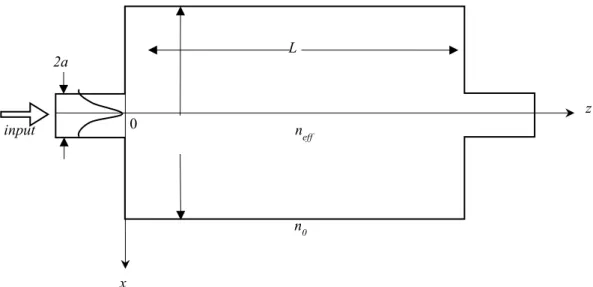
The so-called multimode interferometer (MMI) is actually based on “self-image” phenomenon when multimode interferes with each other inside the waveguide [28-31]. The very simple configuration of an MMI is shown in Fig. 2.1. A multimode waveguide section connected with one/several narrower waveguides is the very basic structure. As shown in the figure, the incident light is injected from the narrow waveguide at left side. After propagating into the multimode section, the light excites into a group of modes. Such different modes interfere with each other, as a result at several position of the multimode section, the “self-image” of the incident field will appear periodically. The duplicate field are almost the same with the incident light. The only differences are the amplitude and the phase condition. In Fig. 2.1, two
Multimode waveguide
Fig. 2.1 Multimode interferometer configuration
duplication of the incident field are illustrated. Be noted that, this duplication always happens whatever the incident modes are.
We care about the position and the phase of duplication in most of the case. By delicate arrangement, the duplicated light phase is controlled, and the optical mode converter are designed [32]. The position and the amplitude of the self-image are actually affected by the mode order, i.e. position or amplitude of self-image are different when incident modes are different. This fact is the most important principle to design the mode-selective light source.
2.2.1 The general principle of self-image in MMI
Figure 2.2 shows the two-dimensional structure of an MMI configuration. We discuss the 2-D MMI structure for simple understanding. The width, thickness and the length of the multimode region are W, 2d and L. The thickness of the waveguide is ignored here. The width of access waveguide connected with the multimode section is 2a. Assuming the effective refractive index of the multimode section is neff and the index of the cladding is n0. The analysis of the 2-D MMI is as follows:
The description for modes inside the multimode waveguide can be written as:
L
x
z 2a
input 0 neff
n0
Fig. 2.2 Two-dimensional representation of an MMI waveguide configuration
E"#(x, y) =
⎩⎪
⎨
⎧ A⎪ #cos 2u#+#56 7 exp :6;=<2x +=67 − jβ#zB (x < −=6) A#cos 26D=<E−#56 7 exp[−jβ#z] (|x| ≤ −=6) A#cos 2u#−#56 7 exp :−6;=<2x −=67 − jβ#zB (x > −=6)
(2.1)
where 𝑢M and 𝜔Mdenote the transverse wave numbers of the m-th mode inside the core and cladding and Am is constant.
This equation group can be solved in the form of:
OPQR
OEP +OOSPQPR+ 𝑘U6𝑛WXX6 𝐸Z = 0 (2.2)
In z direction, for any mode, OPQR
OSP = −𝛽6𝐸Z. In x direction, the form of Ey can be expressed as equation 2.2, we can obtain:
𝑘]6+ 𝛽6 = 𝑘U6𝑛6 (2.3)
For each mode, form 0th mode to ith (i=0, 1, 2, …) mode, k] is written in such form as:
k] =`_ (𝑖 + 1) (2.4)
Then, 𝛽 becomes:
𝛽6 = 𝑘U6𝑛6− 𝑘]6 = 𝑘U6𝑛6− c_(def)` g6 (2.5)
Here (𝑘Uh)6 is much larger than c_(def)` g, then we can express [… ]iPpart as:
:(𝑘Uh)6− c_(def)` gB
i
P = [𝑎6 − 𝑥6]iP = 𝑓(𝑥) (2.7)
as 𝑓(𝑥) can be expressed as:
𝑓(𝑥) = [𝑎6− 𝑥6]f6
𝑓(𝑥)n =1
2(𝑎6− 𝑥6)pf6(−2𝑥) = −𝑥(𝑎6− 𝑥6)pf6
𝑓(𝑥)nn = −(𝑎6 − 𝑥6)pf6− 𝑥 q−1
2(𝑎6 − 𝑥6)pr6(−2𝑥)s
Thus,
𝑓(𝑥) = 𝑓(0) + 𝑓(0)n𝑥 + 𝑓(0)nn ]6P = a −6u]P = 𝑘𝑛WXX −_6vP(def)P
wh`P (2.8)
then,
𝛽 ≈ 𝑘𝑛WXX− c(def)_` g66vhf
yzz (2.9)