Emerging embedded nonvolatile memory solution for ultra low power microcontroller systems
著者 林越 正紀
著者別表示 Hayashikoshi Masanori journal or
publication title
博士論文本文Full 学位授与番号 13301甲第4810号
学位名 博士(工学)
学位授与年月日 2018‑09‑26
URL http://hdl.handle.net/2297/00053018
Creative Commons : 表示 ‑ 非営利 ‑ 改変禁止 http://creativecommons.org/licenses/by‑nc‑nd/3.0/deed.ja
Emerging embedded nonvolatile memory solution for ultra low power
microcontroller systems
超低消費電⼒マイクロコントローラシステムを実現する 次世代不揮発性メモリ応⽤の研究
⾦沢⼤学⼤学院⾃然科学研究科 電⼦情報科学専攻
学籍番号︓1223112005
⽒名︓林越 正紀
主任指導教員名︓新居 浩⼆
2018 年 9 ⽉
Abstract
This thesis reports emerging embedded nonvolatile memory solution for ultra low power microcontroller systems.
Many semiconductor devices are used nowadays. In case of microcontrollers, that with embedded flash memory have become the mainstream and that volume is 70% of all market of microcontroller and the average growth rate of the market is about 16%, compared to the growth rate of all microcontroller market. Thus, the non-volatile memory devices typified by Flash memory are core technologies of all industries. Currently, Flash-MCU has become the mainstream of the microcontrollers. In the future, in which the semiconductor miniaturization, and the greening of society advance, the conventional embedded memory (SRAM, Flash memory) has the technology limitation such as the leakage current problem with the miniaturization of process technology, the next-generation nonvolatile memory (NVRAM) is expected. This study is intended to overcome the challenge of embedded the nonvolatile memory and investigate that solution for ultra-low power microcontroller systems.
For microcontroller systems, critical issues related to embedded nonvolatile memory are pointed out in Chapter 2. The main issues of an embedded nonvolatile memory design are summarized as five limitations: low voltage operation, high endurance characteristic, high speed access, high density, and low leakage current design of system for low power dissipation. An explanation for each limitation is provided to enhance understanding of the study objective.
For the next three parts of this paper, practical nonvolatile memory design techniques against each limitation are demonstrated. In Chapter 3, Capacitor-coupled EEPROM design with capacitor-coupled EEPROM cell and dual-mode sensing scheme for low voltage, high endurance, and high speed access is discussed.
In Chapter 4, practical high density 1T-4MTJ MRAM (Magnetic Random Access Memory) design with 1T-4MTJ cell and voltage-offset self-reference sensing scheme for high endurance, high density, and high speed access is discussed.
In Chapter 5, the zero standby microcontroller system technology with normally-off system architecture and its power management scheme for low voltage operation and low leakage current in point view of hardware and software technologies is discussed.
The overall conclusion of this contribution is presented as a summary in Chapter 6.
Contents
Chapter 1 Introduction ... 1
1.1. Background of research area ... 1
1.2. Objective of this study ... 2
1.3. Overview of this thesis ... 4
Chapter 2 Issue of embedded nonvolatile memory for low power microcontroller systems ... 7
2.1. Introduction ... 7
2.1.1. Flash memory ... 8
2.1.2. Nonvolatile RAM ... 9
2.2. Low voltage operation ... 12
2.3. High reliability ... 12
2.4. High speed access ... 12
2.5. High density ... 13
2.6. Low standby leakage current ... 13
2.7. Summary ... 15
Chapter 3 A dual-mode sensing scheme of capacitor-coupled EEPROM cell ... 17
3.1. Introduction ... 17
3.2. Capacitor-coupled EEPROM cell ... 18
3.2.1. Memory cell structure ... 18
3.2.2. Memory cell operation ... 18
3.3. Dual-mode sensing (DMS) scheme ... 21
3.3.1. Sensing operation ... 21
3.3.2. Load transistor optimization ... 23
3.3.3. Array architecture ... 23
3.3.4. Soft error Immunity ... 25
3.4. Simulated results ... 25
3.4.1. Sensing speed enhancement ... 25
3.4.2. Endurance improvement ... 25
3.5. Summary ... 29
Chapter 4 A high-density and high-speed 1T-4MTJ MRAM with voltage offset self-reference sensing scheme ... 31
4.1. Introduction ... 31
4.2. 1T-4MTJ memory cell structure ... 33
4.3. Voltage offset self-reference sensing scheme ... 36
4.3.1. Concept of read-out scheme for 1T-4MTJ cell ... 36
iv
4.3.2. SRSV read-out sense amplifier ... 38
4.3.3. Simulation results ... 40
4.4. Test chip implementation and evaluation ... 42
4.5. Hybrid embedded MRAM solution with 1T-1MTJ and 1T-4MTJ cells ... 47
4.6. Summary ... 49
Chapter 5 Low-power multi-sensor system with power management and nonvolatile memory access control for IoT applications ... 51
5.1. Introduction ... 51
5.2. Normally-off architecture for low-power multi- sensor systems ... 53
5.2.1. Key technology of Normally-off computing ... 53
5.2.2. Normally-of multi-sensor systems ... 54
5.2.3. Hierarchical power gating control with activity localization ... 56
5.3. Normally-off power management method ... 58
5.3.1. Task scheduling technology ... 58
5.3.2. Autonomous standby mode transition technology ... 59
5.4. Nonvolatile memory access control technology ... 62
5.5. Evaluation result ... 66
5.6. Summary ... 72
Chapter 6 Conclusion ... 73
References ... 75
Publications ... 81
Acknowledgements ... 89
List of figures
Figure 1.1: Market overview of microcontrollers Figure 1.2: MCU applications and market volume
Figure 1.3: Trend of microcontroller with embedded nonvolatile memory Figure 1.4: Outline of this thesis
Figure 2.1: Comparison of microcontroller depend on embedded memory Figure 2.2: Operating mechanism of Flash memory
Figure 2.3: Nonvolatile memory summary Figure 2.4: Operating principle of MRAM cell
Figure 2.5: Comparison of Field-MRAM cell and STT-MRAM cell Figure 2.6: Trend of microcontroller with embedded Nonvolatile memory Figure 2.7: Trend of dynamic power and sub-threshold leakage dissipation Figure 2.8: Paradigm shift for power savings
Figure 3.1: A newly proposed capacitor-coupled EEPROM cell.
(a) A memory cell circuit, (b) A cross sectional view Figure 3.2: The equivalent circuits in the standby state.
(a) The memory cell storing “H” data. (b) The memory cell storing “L” data.
Figure 3.3: “H” data sensing operation.
(a) The memory cell circuit of DMS scheme. (b) The waveforms of readout voltage.
Figure 3.4: “L” data sensing operation.
(a) The memory cell circuit of DMS scheme. (b) The waveforms of readout voltage.
Figure 3.5: The memory cell array architecture using the DMS scheme Figure 3.6: The clock timing diagram
Figure 3.7: A simulated signal amplitude on the bit line. The simulation was carried out with a 3V power supply, a cell current of 15 uA, a bit-line capacitance of 250 fF, and Cs capacitance of 25fF.
Figure 3.8: The cell current dependence of the access time.
Figure 3.9: The general endurance characteristics corresponding to the 1-Mb level EEPROM memory transistor.
Figure 3.10: The estimated endurance characteristics in the case of the low voltage and short
time programming.
vi
Figure 4.1: Circuit and layout diagrams of Field MRAM and STT MRAM Figure 4.2: Cell size trend of Field-MRAM and STT-MRAM
Figure 4.3: Birds views of MRAM memory cell structures with conventional 1T-1MTJ and proposed 1T-4MTJ
Figure 4.4: Top view SEM photograph of 1T-4MTJ in 130 nm technology Figure 4.5: Concept of readout scheme for 1T-4MTJ cell
Figure 4.6: SRSV sensing circuit
Figure 4.7: Self-reference amplifier portion of SRSV Figure 4.8: Data Amplifier portion of SRSV
Figure 4.9: Simulation waveform of the readout operation (@MR=40%, RMTJ(data"0")=40Kohm)
Figure 4.10: Read current of 1T-1MTJ and 1T-4MTJ MRAM (x16 bits word organization)
Figure 4.11: Block diagram of proposal embedded WWL driver Figure 4.12: Layout of proposal embedded WWL driver
Figure 4.13: Array area comparison
Figure 4.14: Block diagram of 1Mbit MRAM core Figure 4.15: 1Mb MRAM micrograph
Figure 4.16: Measurement result of 1T-4MTJ cell (VCC versus Read time shmoo plot)
Figure 4.17: MCU chip image of on-chip hierarchical MRAM solution
Figure 4.18: Chip area reduction effect of on-chip hierarchical MRAM solution Figure 5.1: The relationship between the power consumption and the number of nodes Figure 5.2: Activity localization for efficient normally-off computing by task scheduling Figure 5.3: System diagram of normally-off multi-sensor node
Figure 5.4: Concept of hierarchical power gating (PG) control
Figure 5.5: Simulation results of proposal hierarchical power-gating (PG) control in case of fire alarm system
Figure 5.6: MCU switching task scheduling
Figure 5.7: Difference in Energy consumption of using each standby modes, which are idle mode, three level standby modes (deep sleep, normal sleep, light sleep), and power off mode of industrial available MCU [43].
Figure 5.8: Concept of proposed NVM architecture
Figure 5.9: Block diagram of nonvolatile memory access controller Figure 5.10: Intruder detection system
Figure 5.11: Outline of intruder detection evaluation system
Figure 5.12: Block diagram of evaluation board
Figure 5.13: Photograph of evaluation board
Figure 5.14: Task flow of intruder detection system
Figure 5.15: Evaluation results
List of tables
Table 3.1: The voltage conditions in the write, standby, and read operations:
(a) Conventional and (b) Proposed.
Table 4.1: Technology feature of 1Mb-MRAM test chip
Table 5.1: Available standby modes of Renesas 32-bit MCU: RX63N [62]
Table 5.2: Each state of IR sensor and motion sensor depends on distance of approaching object Table 5.3: Breakdown of energy consumption at intruder system evaluation
Table 5.4: Selected appropriate standby mode of MCU according to distance of approaching at
this use case
Chapter 1 Introduction
1.1. Background of research area
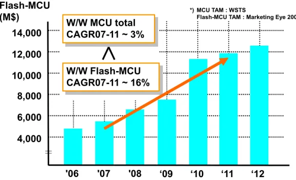
Many semiconductor devices are used nowadays. In case of microcontrollers, that with embedded flash memory have become the mainstream and that volume is 70% of all market of microcontrollers. The market overview of microcontrollers is shown in Figure 1.1. The average growth rate of the market is about 16%, compared to the growth rate of all microcontroller market, it has remained at a high rate. Thus, the non-volatile memory devices typified by Flash memory are core technologies of all industries. Microcontroller applications and market volume is shown in Figure 1.2. Thus, nonvolatile memory is embedded to almost of microcontroller devices.
*) MCU TAM : WSTS
Flash-MCU TAM : Marketing Eye 2007-2011
Flash-MCU (M$)
10,000 12,000 14,000
'06 '07 '08 ‘09 ‘10 4,000
6,000 8,000
‘11 ‘12 W/W Flash-MCU
CAGR07-11 ~ 16%
W/W MCU total CAGR07-11 ~ 3%
Figure 1.1: Market overview of microcontrollers
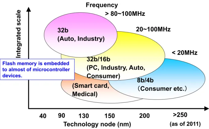
2
32b
(Auto, Industry)
> 80~100MHz
20~100MHz
< 20MHz 32b/16b
(PC, Industry, Auto, Consumer)
8b/4b
( Consumer etc. )
Integrated scale
Technology node (nm)
130 150 200 >250
Frequency
(as of 2011) (Smart card,
Medical)
40 90
Flash memory is embedded to almost of microcontroller devices.
Figure 1.2: MCU applications and market volume
1.2. Objective of this study
As mentioned in previous chapter, nonvolatile memory is a key device for recent microcontroller systems. The trend of microcontroller with embedded nonvolatile memory is shown in Figure 1.3.
Through ’80 years from the end of the ’70s, it appeared single-chip microcontroller with
embedded mask ROM, and it becomes possible to make the generalization with instruction sets
architecture and real time control. Thereby, it has made a big evolution in terms of performance
and ease of use. In the late of ’80s, it appeared the microcontroller with EPROM (Erasable
Programmable Read Only Memory) or OTP (One Time Programmable read only memory), and it
becomes possible to write the program data at production stage by user. Thereby, the
development and production cost has been greatly improved. After then, in the half of ’90s, it
appeared the microcontroller with embedded Flash memory (Flash-MCU), and it becomes
possible to rewrite the program data after production. Thereby, a mass production setup has
become possible at program development completion and the development period has become
enabled to be shorten. In addition, a big change has been happened on production and distribution cost side because of commonization of microcontrollers. Currently, Flash-MCU has become the mainstream of the microcontrollers. In the future, in which the semiconductor miniaturization, and the greening of society advance, the conventional embedded memory (SRAM, Flash memory) has the technology limitation such as the leakage current problem with the miniaturization of process technology, the next-generation nonvolatile memory (NVRAM) is expected.
This study is intended to overcome the challenge of embedded the nonvolatile memory and investigate that solution for ultra-low power microcontroller systems.
1980 1990 2000 2010
MASK CPU -ROM
Periph. RAM
EP- CPU ROM
Periph. RAM
Flash Memory CPU
Periph. RAM
NV-RAM CPU
Periph.
Single Chip MCU with Mask ROM
Embedded EPROM or OTP
Embedded Flash Memory
Embedded Nonvolatile RAM
2020
- Write program at production, - Enable to reduce
the development and production costs.
- Generalization with instruction sets architecture - Real time control
- Rewrite program after production, - Enable to reduce
the development time.
- Unified Memory, - Enable to reduce
standby current.
- Instant on/off, - Possible for
create new application (Zero standby application)
Figure 1.3: Trend of microcontroller with embedded nonvolatile memory
4
1.3. Overview of this thesis
Figure 1.4 presents the outline of this thesis, as visualized very simply. First, the background and objective of this study are described. For microcontroller systems, critical issues related to embedded nonvolatile memory are pointed out in Chapter 2. The main issues of an embedded nonvolatile memory design are summarized as five limitations: low voltage operation, high endurance characteristic, high speed access, high density, and low power consumption energy design of system for low power dissipation. An explanation for each limitation is provided to enhance understanding of the study objective.
Chapter 2
Challenge of embedded nonvolatile memory for microcontrollers
2. High endurance 3. High speed access 4. High density
Chapter 3
Approach of Capacitor-coupled Flash memory - Capacitor-coupled cell
- Dual-mode sensing scheme Chapter 4
Approach of high density 1T-4MTJ MRAM - High density 1T-4MTJ cell
- Voltage-offset self-reference sensing scheme - Hierarchical embedded MRAM architecture Chapter 5
Approach of Zero standby microcontroller system - Architecture with Normally-off technology - Power management technology
- Task scheduling
- Autonomous standby mode transition control - Nonvolatile memory access control
5. Low energy consumption 1. Low voltage operation
Figure 1.4: Outline of this thesis
For the next three parts of this paper, practical nonvolatile memory design techniques against
each limitation are demonstrated. In Chapter 3, Capacitor-coupled EEPROM design with
capacitor-coupled EEPROM cell and dual-mode sensing scheme for low voltage, high endurance,
and high speed access is discussed.
In Chapter 4, practical high density 1T-4MTJ MRAM (Magnetic Random Access Memory) design with 1T-4MTJ cell and voltage-offset self-reference sensing scheme for high endurance, high density, and high speed access is discussed.
In Chapter 5, the zero standby microcontroller system technology with normally-off system architecture and its power management scheme for low voltage operation and low leakage current in point view of hardware and software technologies is discussed.
The overall conclusion of this contribution is presented as a summary in Chapter 6.
Chapter 2 Issue of embedded nonvolatile memory for low power microcontroller systems
In chapter 2, the comparison of microcontroller depends on the kinds of embedded nonvolatile memory and issue for realizing the future low power microcontroller systems.
2.1. Introduction
The comparison of microcontroller depends on the kinds of embedded nonvolatile memory such as Flash memory and Nonvolatile RAM (NVRAM) is shown in Figure 2.1. As mentioned in chapter 1.2, Flash-MCU has become the mainstream of the microcontrollers now, and in future, NVRAM is expected because of technology limitation of conventional embedded memory (SRAM, Flash memory) such as the leakage current problem with the miniaturization of process technology. In case of microcontroller with embedded NVRAM, NVRAM is used as universal memory, which is act as both RAM and ROM, because of high-speed random accessibility.
ROM
(Flash Memory) CPU
RAM (SRAM)
Periph.
Microcontroller with Embedded Flash Memory
Microcontroller with
Nonvolatile RAM (NVRAM)
Universal memory (NVRAM) CPU
Periph.
RAM (SRAM)
Figure 2.1: Comparison of microcontroller depend on embedded memory
8
2.1.1. Flash memory
The operating mechanism of Flash memory is shown in Figure 2.2. The memory transistor of Flash memory is formed with the control gate (CG) and floating gate (FG) through tunnel oxide.
And threshold voltage (Vth) of memory transistor is decided with the number of electron injected to FG. Therefore, Flash memory needs high voltage to inject or release electron to/from FG, and write cycle endurance is limited because of the damage to tunnel oxide caused by injecting or releasing electron to/from FG.
MOS Tr. Flash memory
- Vth constant
- Vth is decided at wafer process
Vth distribution Vth
0V
Vth
"1"
"0"
Vth distribution
FG
Gate
Read Vgate - Vth variable
- Vth is decided by the number of electron injected to floating gate (FG)
0V
CG Tunnel oxide
Figure 2.2: Operating mechanism of Flash memory
2.1.2. Nonvolatile RAM
The summary of characteristics of various nonvolatile RAM is shown in Figure 2.3. A Feature, which is expected in the next-generation non-volatile memory as embedded memory is a coexistence of high speed accessibility as RAM and non-volatility of Flash memory.
PRAM FeRAM MRAM
ReRAM Flash
memory SRAM
Field STT
Cell read non-destructive destructive non-destructive non-destructive non-destructive non-destructive non-destructive Material Chalcogenide
(GeSbTe) PZT CoFe Chalcogenide
(GeSbTe)
Metal-oxide
(TaO) Si Pure CMOS
Cell Area
(F2) 6~20 20~40 10~30 6~20 ~30 20~30 120
Write
access 0.1s~1ms <50ns <10ns < 10ns <50ns 30μs 5ns
Read
access <20ns <50ns <10ns < 10ns <50ns 10~30ns 5ns
Write # 1012 108~1012 1016(∞) 1016(∞) 102~109 105 ∞
High
Voltage No No No No No Need No
Pros. • Simple structure
• Slow write • Middle-speed
• Fast read/write
• Universal memory
• Fast read/write
• Universal memory
• Fast read/write
• Simple
structure • Fast read
• Fast read/write
• Pure CMOS
• Write# free
Cons. • Thermal disturb
• Write# limit
• Scaling limt
• Read# limit
• Write# limit
• Magnetic field
disturb • Read disturb • Forming
• Write# limit
• High voltage
• Slow write
• Write# limit
• Soft error
• Leakage
• Cell area
Figure 2.3: Nonvolatile memory summary
10
Here, MRAM, which is expected for embedded NVRAM to microcontrollers, is explained for example. The operating principle of MRAM cell is shown in Figure 2.4. MRAM cell is constituted by one magnetic Tunnel Junction (MTJ) element and one transistors. MTJ element includes a fixed ferromagnetic layer, tunnel barrier and free ferromagnetic layer. The free magnetic moment is engineered to have two stable states, parallel (0) and anti-parallel (1) to the reference moment. The change in tunneling resistance between states is characterized by the parameter Magneto Resistance (MR), defined by R1=R0*(1+MR). In write operation, the magnetic direction of ferromagnetic film is inverted by the synthetic current magnetic field of Bit Line (BL) and Write Word Line (WWL). This direction should be determined by the direction of bit line current. In read operation, the resistance value of MTJ is detected with the difference of read current through MRAM cell.
HWWL HBL
Magnetic field of BL (HBL)
Bit-line (BL)
Write word-line (WWL)
MTJ element
Write operation:
Invert the magnetic direction of ferromagnetic film with the synthetic magnetic field of BL and WWL.
Write
Magnetic field of WWL (HWWL)
Bit-line (BL)
Word-line (WL) Read
Free layer Fixed Layer Small
resistance
Tunnel Film MTJ
element Read operation:
Detect the resistance value of MTJ.
BL WWL WL
D G S
Large resistance Magnetic field of BL (HBL)
Magnetic field of WWL (HWWL)
Figure 2.4: Operating principle of MRAM cell
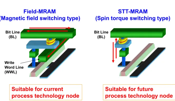
The comparison of Filed-MRAM cell and STT-MRAM cell is shown in Figure 2.5. Whereas the write operation of Field-MRAM cell is done by the synthetic current magnetic field of BL and WWL, the write operation of STT-MRAM cell is done by the spin torque caused by current flow through MTJ element. This direction of free ferromagnetic layer should be determined by the direction of that current flow. That current value is reduced depends on MTJ size. Therefore, STT-MRAM is suitable for future process technology node.
Field-MRAM
(Magnetic field switching type)
STT-MRAM
(Spin torque switching type)
Bit Line (BL)
Write Word Line (WWL)
Bit Line (BL)
Suitable for future
process technology node Suitable for current
process technology node
Figure 2.5: Comparison of Field-MRAM cell and STT-MRAM cell
12
2.2. Low voltage operation
As mentioned in chapter 2.1.1, Flash memory needs high voltage to inject or release electron to/from FG. Flash memory has on-chip high voltage (around 10 V) generator, which should be generated with power supply voltage (Vcc). However, Vcc has become lower with the miniaturization of process and it becomes difficult to generate high voltage level with high efficiency. Furthermore, other circuits in microcontroller do not need the high voltage level.
Therefore, low voltage operation is important issue at embedded nonvolatile memory for microcontroller.
2.3. High reliability
The comparison of write cycle endurance is shown in Figure 2.3. As mentioned in chapter 2.1.1, the write cycle endurance of Flash memory is limited because of the damage to tunnel oxide caused by injecting or releasing electron to/from FG. Actual characteristic of write cycle endurance is around 10
4~6cycles. So, in case of Flash memory, write cycle endurance is need to improve for embedded use to microcontrollers. On the other hand, the write cycle endurance of NVRAM such as MRAM is no limited, and the other NVRAMs such as PRAM (Phase change Random Access Memory), FeRAM (Ferroelectric Random Access Memory), and ReRAM (Resistance Random Access Memory) are under device improving.
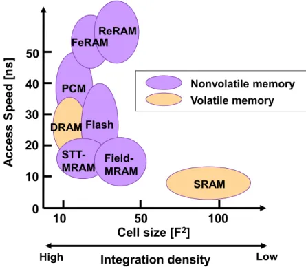
2.4. High speed access
The trend of microcontroller with embedded nonvolatile memory is shown in Figure 2.6. In case
of current volatile memory such as SRAM, though it has high speed accessibility of 5~10ns, it
has no availability for high density integration. In case of Flash memory, access speed is not so
high compared with NVRAM such as MRAM. For use embedded memory for microcontroller, it
needs the access speed enhancement.
Cell size [F2]
Access Speed [ns]
100
10 50
0 10 20 30 40 50
PCM
ReRAM FeRAM
High
Volatile memory Nonvolatile memory
SRAM Flash
DRAM STT-
MRAM Field- MRAM
Integration density Low
Figure 2.6: Trend of microcontroller with embedded Nonvolatile memory
2.5. High density
The trend of microcontroller with embedded nonvolatile memory is shown in Figure 2.6. In case of current volatile memory such as SRAM, though it has high speed accessibility of 5~10ns, it has no availability for high density integration. Therefore, cell size reduction is required for use of embedded memory to microcontrollers. Especially, in case Field-MRAM, cell size is larger than Flash memory. So, it needs cell size reduction for replacing high density ROM area.
2.6. Low standby leakage current
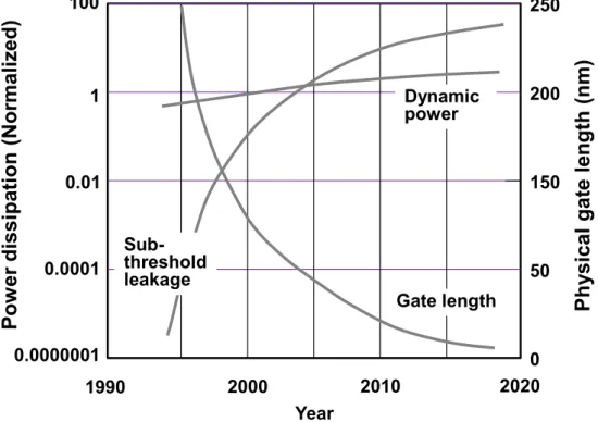
The trend of dynamic power and sub-threshold leakage dissipation is shown in Figure 2.7. The
gate length becomes smaller with the miniaturization of process, and as the results, the
subthreshold leakage power is increased with the miniaturization of process. It becomes much
important the standby power reduction not only process level but also system level for future
ultra-low power microcontroller systems.
14
100
1
0.01
0.0001
0.0000001
Pow er dissipation (Normalized) Phy sical g ate length (nm)
250
200
150
50
0 Dynamic
power
1990 2000 2010 2020
Year
Gate length Sub-threshold
leakage
Figure 2.7: Trend of dynamic power and sub-threshold leakage dissipation
power
time active standby
Large SRAM standby leak
SRAM based operation
power
time active standby
Flash start-up
Flash based operation
Data evacuation to Flash memory
power
time active standby
NVRAM based operation
<Features>
- Fast power-on/off
- No DC current during standby
Figure 2.8: Paradigm shift for power savings
Paradigm shift for power savings with embedded NVMRM is shown in Figure 2.8. The current embedded memories used in the microcontroller such as SRAM and Flash memory have the leakage current of SRAM due to process miniaturization and the overhead time and power consumption to restore data from Flash memory at power-on period. It is possible to overcome the above problems by the NVRAM, and realize very low power operation with frequent intermittent operation and high reliability of peripheral circuits with full power-off standby operation. [1]
2.7. Summary
To realize the embedded nonvolatile memory solution for ultra-low power microcontroller
systems, it should be overcome above mentioned challenges, which are low voltage operation,
high reliability, high speed access, high density, low standby leakage current. In this thesis,
author’s approach to overcome the challenge of embedded the nonvolatile memory and
investigate that solution for ultra-low power microcontroller systems.
Chapter 3 A dual-mode sensing scheme of capacitor- coupled EEPROM cell
This chapter describes a dual-mode sensing (DMS) scheme of a capacitor-coupled EEPROM cell.
A new memory cell structure and a new sensing scheme are proposed and estimated. The new memory cell combines an EEPROM cell with a DRAM cell. The DMS scheme utilizes the charge-mode sensing of the DRAM cell in addition to the current-mode sensing of the EEPROM cell. Using this DMS technique, the sensing speed can be enhanced by 36% at a cell current of 15 FA by virtue of the additional charge-mode sensing. Furthermore, the stress applied to the tunnel oxide of the memory transistor can be relieved by decreasing the programming voltage and shortening the programming time. Therefore, with this memory cell structure and sensing scheme, it is possible to realize high-speed sensing in low-voltage operation and high endurance.
3.1. Introduction
There have been many types of memory cell structures and memory cell array architectures for EEPROM’s proposed [2-5]. For use in the memory cards of hand-held computers, low-voltage operation and high endurance are the most important design issues for high-performance EEPROM’s [6-7]. In low-voltage operation, the sensing speed and sensing margin are degraded.
For high endurance, the stress applied to the tunnel oxide of the memory transistor must be relieved [8-10]. Decreasing the programming voltage and shortening the programming time are effective in improving the endurance characteristics. However, low voltage and short time programming decrease the cell current. The small cell current also degrades the sensing speed and sensing margin. To overcome these problems, we propose a capacitor-coupled EEPROM cell and a dual-mode sensing (DMS) scheme [11].
The capacitor-coupled EEPROM cell combines an EEPROM cell with a DRAM cell. The DMS scheme utilizes the charge-mode sensing of the DRAM cell in addition to the current-mode sensing of the EEPROM cell. The current-mode sensing is based on the previously proposed dynamic sensing schemes utilizing differential sensing and source biasing techniques [12-13].
In this paper, a capacitor-coupled EEPROM cell and a DMS scheme are proposed. In chapter 3.2, a newly proposed capacitor-coupled EEPROM cell and its operation are described.
In chapter 3.3, the concept of the DMS scheme and its operation are described, and the memory
cell array architecture using this scheme is shown. In chapter 3.4, the enhancement of the sensing
speed is described, and the possibility of endurance improvement is discussed. Finally, a
conclusion is given in chapter 3.5.
18
3.2. Capacitor-coupled EEPROM cell
3.2.1. Memory cell structure
A memory cell circuit of the newly proposed capacitor-coupled EEPROM cell is shown in Figure 3.l (a). This memory cell combines an EEPROM cell with a DRAM cell. In the capacitor-coupled EEPROM cell, the DRAM cell enhances the sensing speed and the EEPROM cell holds the data stored in the DRAM cell. Thus, the refresh operation for the DRAM cell is eliminated.
The memory cell is composed of a select transistor ST, a memory transistor MT of the floating-gate-type EEPROM cell, and a capacitor Cs. Cs is formed between the drain and the control gate of MT. Cs acts as the storage capacitor of the DRAM cell. The signal charge corresponding to the data written in MT is also stored in Cs.
As an example, a cross-sectional view of a capacitor-coupled EEPROM cell with a three-dimensional structure is shown in Figure 3.l (b). By adding a storage-node polysilicon layer to the conventional EEPROM process, the cell area increase due to the additional capacitor can be minimized. The additional capacitor Cs is formed between the storage-node polysilicon layer and the control-gate polysilicon layer. The cell area penalty is estimated to be less than 10%
compared with the conventional EEPROM cell by using this simple process technology.
3.2.2. Memory cell operation
The voltage conditions in the write, standby, and read operations are shown in Table I. The write operation is carried out in a conventional EEPROM manner. To written “H” data, bit line BL and word line WL are pulled up to a high voltage Vpp, control gate line CGL is grounded, and source line SL is set floating. Thus, the electrons are transferred from the floating gate to the drain through the tunnel oxide of MT, and MT goes into the depletion state.
The equivalent circuit of the memory cell storing an
“H” data in the standby state is shown inFigure 3.2 (a). In the standby state, SL goes to the Vcc level and CGL is grounded. As MT is in the depletion state, the storage node of Cs is charged to the Vcc level and kept “H” through the channel resistance R of MT. Thus, SL is kept at the Vcc level in contrast with the conventional EEPROM cell, and the “H” data stored in Cs is kept by MT in the depletion state. Therefore, there is no need for refreshing the data stored in Cs.
To write “L” data, WL and CGL are pulled up to high voltage VPP, and BL and SL are
grounded. Thus, the electrons are transferred from the drain to the floating gate through the tunnel oxide of MT, and MT enters the enhancement state. The MT drain is grounded through BL, and the storage node of Cs is discharged to the ground level.
The equivalent circuit of the memory cell storing “L” data in the standby state is shown in Figure 3.2 (b). As MT is in the enhancement state, the storage node of Cs is kept “L” floating.
During the standby state. the “L” data is kept by the leakage current to the substrate as usual DRAM operation. Therefore, the capacitor-coupled EEPROM cell is a kind of DRAM cell combined with an EEPROM cell.
Figure 3.1: A newly proposed capacitor-coupled EEPROM cell.
(a) A memory cell circuit. (b) A cross sectional view.
20
Table 3.1: The voltage conditions in the write, standby, and read operations:
(a) Conventional and (b) Proposed.
Figure 3.2: The equivalent circuits in the standby state.
(a) The memory cell storing “H” data. (b) The memory cell storing “L” data.
3.3. Dual-mode sensing (DMS) scheme
3.3.1. Sensing operation
The proposed DMS scheme suitable for the capacitor-coupled EEPROM cell is described.
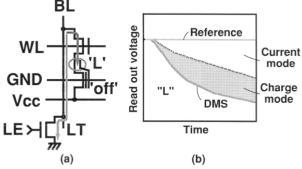
The memory cell circuit of the DMS scheme and its waveforms of readout voltage in the case of sensing “H” data are shown in Figure 3.3 (a) and (b), respectively. In consideration of low-voltage operation, Vcc is defined as 3 V in the DMS operation. In the read operation, SL is kept at the Vcc level and CGL is grounded. In the standby state, BL is precharged to the Vcc/2 level, which is equal to 1.5 V. This precharge level of BL is low enough to prevent the decrease of the charge stored in the MT floating gate caused by the inverse electric field applied to the tunnel oxide. Thus, this read disturbance problem can be avoided by the Vcc/2 precharging of BL in the DMS scheme. As MT is in the depletion state, the storage node of Cs is kept “H” by MT as described previously. In the active cycle, WL is selected and BL is pulled down through the load transistor LT. The charge stored in Cs is transferred to BL, and BL goes high rapidly. This operation is the charge-mode sensing. Simultaneously, BL is charged through MT, and goes still higher. This operation is the current-mode sensing.
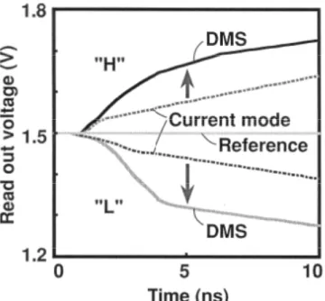
The DMS operation has two modes of sensing. The solid line in Figure 3.3 (b) shows the waveform of readout voltage in the DMS scheme, and the broken line shows that in the current-mode only sensing. The signal amplitude in the DMS scheme is increased compared with the current-mode only sensing. The shadowed part corresponds to the improvement of the signal amplitude by virtue of the additional charge-mode sensing.
The memory cell circuit of the DMS scheme and its waveforms of readout voltage in the
case of sensing ”L“ data are shown in Figure 3.4 (a) and (b), respectively. As MT is in the
enhancement state, the storage node of Cs is kept in the “L” floating state. In the active cycle,
WL is selected. The charge stored in the BL capacitance is transferred to Cs and BL goes low
rapidly. Simultaneously, BL is discharged through LT, and goes still lower. As well as the case of
sensing “H” data, the shadowed part corresponds to the improvement of the signal amplitude by
virtue of the additional charge-mode sensing. Therefore, this charge-mode sensing increases the
signal amplitude of readout voltage and enhances the sensing speed.
22
Figure 3.3: “H” data sensing operation.
(a) The memory cell circuit of DMS scheme. (b) The waveforms of readout voltage.
Figure 3.4: “L” data sensing operation.
(a) The memory cell circuit of DMS scheme. (b) The waveforms of readout voltage.
3.3.2. Load transistor optimization
The optimization of the LT size is a key point in the ideal DMS operation. In the standby state, BL is precharged to the Vcc/2 level. When the “L” datum is sensed, MT is in the enhancement state, and BL is pulled down to the ground level through LT. When the “H” data is sensed, MT is in the depletion state, and BL is pulled up to the Vcc level through MT and ST.
However, LT is also in the ON state, and the “H” level of BL is determined by the ratio of the cell current to the current drive capacity of LT. The transistor size of LT should be optimized to equalize the “H” sensing speed to the “L” sensing speed. Here, the current drive capacity of the memory cell and LT are denoted as Ids and I
LT, respectively, as it is shown in Figure 3.3 (a). The transistor size of LT is optimized so that I
LTis equal to Ids/2.
3.3.3. Array architecture
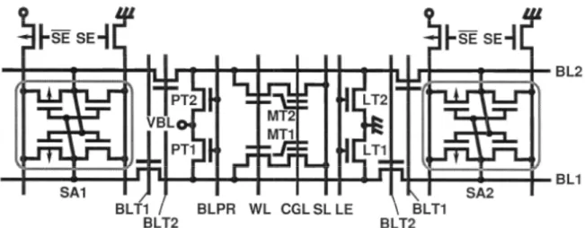
The memory cell array architecture using the DMS scheme is shown in Figure 3.5, and the clock timing diagram is shown in Figure 3.6. In Figure 3.5, VBL is equal to the Vcc/2 level.
Sense amplifiers SA1 and SA2 are located alternately at both ends of bit lines BL1 and BL2 to relax the layout pitch of sense amplifiers. The bit-line precharge transistors PTl and PT2 and the load transistors LTl and LT2 are connected to bit lines BL1 and BL2, respectively.
In the read operation, BLT2 goes “L,” and BL1 and BL2 are disconnected from SA2 and SAl, respectively. This architecture is similar to the open bit-line scheme of the DRAM. The datum written in the memory transistor MT1 is sensed and latched by the sense amplifier SA1, as well as the datum in MT2 by the sense amplifier SA2.
In the differential sensing cycle, BLTl goes “L,” and BLl and BL2 are disconnected from SA1 and SA2, respectively. Thus, the datum written in the memory transistor is sensed by the isolated sensing manner to enhance the sensing speed.
In the restore cycle, BLTl goes “H,” and BLl and BL2 are reconnected to SA1 and SA2, respectively. In this cycle, when the memory transistor is in the depletion state, the storage node of the capacitor is charged to the Vcc-Vth level through the sense amplifier and then it is charged to the full Vcc level by the memory transistor in the depletion state. Thus BLTl does not have to be boosted to write full Vcc level data.
This architecture offers a practical implementation of the DMS scheme, which is suitable for
a high-performance EEPROM array.
24
Figure 3.5: The memory cell array architecture using the DMS scheme
Figure 3.6: The clock timing diagram
3.3.4. Soft error Immunity
In the case of the DRAM cell, the alpha-particle-induced soft error problem is the important issue. Using the proposed capacitor-coupled EEPROM cell, the decrease of the charge stored in Cs caused by collecting the alphaparticle-induced charge is compensated by MT. Therefore, the cell mode of the soft error does not occur, and the soft error rate is improved compared with usual DRAM operation.
Furthermore, the bit-line mode of the soft error is important in the dynamic sensing scheme.
Using this DMS technique, the signal amplitude on the bit line is increased by virtue of the additional charge-mode sensing. Therefore, the bit-line mode of the soft error is also improved.
3.4. Simulated results
3.4.1. Sensing speed enhancement
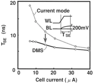
A simulated signal amplitude on the bit line is shown in Figure 3.7. This simulation was carried out with a 3V power supply, a cell current of 15 uA, a bit-line capacitance of 250 fF, and Cs capacitance of 25 fF. The signal amplitude in the DMS scheme is increased by 100 mV at 5 ns after word-line selection, which is a 120% improvement compared with the current-mode only sensing. Thus, the high-speed sensing is realized.
The cell current dependence of the access time is shown in Figure 3.8. Here, TSE is defined as the period to obtain the signal amplitude of 200 mV after the word line is activated. In the proposed DMS scheme, TSE is improved by 36% at the cell current of 15 uA by virtue of the additional charge mode sensing.
This DMS scheme has two merits. One is the enhancement of the sensing speed at the same cell current of the memory transistor. The other is the decrease of the cell current to obtain the same sensing speed compared with the current-mode only sensing scheme.
3.4.2. Endurance improvement
In consideration of above merits, the possibility of endurance improvement is discussed. As
26
both programming and erasing operations are carried out through the tunnel oxide, the endurance characteristics of the memory transistor are very important. The general endurance characteristics corresponding to the 1-Mb level EEPROM memory transistor are shown in Figure 3.9. Here, the horizontal axis shows the erase-program cycles. The upper vertical axis shows the threshold voltage of the memory transistor in the enhancement state, and the lower vertical axis shows the cell current of the memory transistor in the depletion state. In Figure 3.9, the window narrowing caused by the charge trapping in the tunnel oxide of the memory transistor appears at a higher cycle limit. This window narrowing degrades the sensing margin and the sensing speed. It was defined that the sensing operation is achieved normally until TSE is equal to 10 ns. The cell current required for the current-mode only sensing should be more than 17 uA. Thus, endurance is limited to l0
5cycles. On the other hand, using the DMS technique, the sensing speed is hardly degraded with the decrease of the cell current. Thus, the endurance characteristics are improved compared with those in the current-mode only sensing. Assuming that an intrinsic breakdown of the tunnel oxide can be extended, the DMS scheme has a possibility to improve the endurance characteristics in spite of the window narrowing.
Figure 3.7: A simulated signal amplitude on the bit line. The simulation was carried out with a 3V power supply, a cell current of 15 uA, a bit-line capacitance of 250 fF, and Cs capacitance of
25fF.
Figure 3.8: The cell current dependence of the access time.
Next, the possibility of endurance improvement is discussed from another point of view. For high endurance, the stress applied to the tunnel oxide of the memory transistor must be relieved.
Decreasing the programming voltage and shortening the programming time are effective in
improving the endurance characteristics. The estimated endurance characteristics in the case of
low voltage and short time programming are shown in Figure 3.10. It is defined that TSE for
sensing successfully is more than 8 ns. Using the DMS technique, the cell current can be
decreased by 12 uA at TSE of 8 ns, which is a 55 % improvement compared with the
current-mode only sensing. The threshold voltage can be also decreased while the leakage current
through the memory transistor is prevented. Thus, the stress of the tunnel oxide is relieved
compared with that in the current-mode only sensing scheme. Therefore, the endurance
characteristics can be improved.
28
Figure 3.9: The general endurance characteristics corresponding to the 1-Mb level EEPROM memory transistor.
Figure 3.10: The estimated endurance characteristics in the case of the low voltage and short time
programming.
3.5. Summary
A capacitor-coupled EEPROM cell and a dual-mode sensing (DMS) scheme are proposed and estimated. This memory cell combines an EEPROM cell with a DRAM cell, and the cell area penalty is estimated to be less than 10% compared with the conventional EEPROM cell. Using this DMS technique, the signal amplitude on the bit line is increased by 120% at 5 ns after word-line selection, and the sensing speed is enhanced by 36% at the cell current of 15 uA by virtue of the additional charge-mode sensing. Furthermore, the cell current can be decreased by 55% compared with the current-mode only sensing scheme. Therefore, the stress applied to the tunnel oxide of the memory transistor can be relieved by decreasing the programming voltage and shortening the programming time, and it is possible to improve the endurance characteristics.
With this memory cell structure and sensing scheme, it is possible to realize high-speed
sensing in low-voltage operation and high endurance. The capacitor-coupled EEPROM cell and
the DMS scheme are promising candidates for high-performance EEPROM’s.
Chapter 4 A high-density and high-speed 1T-4MTJ MRAM with voltage offset self-reference sensing scheme
A 1-Transistor 4-Magnetic Tunnel Junction (1T-4MTJ) memory cell has been proposed for field type of Magnetic Random Access Memory (MRAM). Proposed 1T-4MTJ memory cell array is achieved 44% higher density than that of conventional 1T-1MTJ thanks to the common access transistor structure in a 4-bit memory cell. We also proposed a self-reference sensing scheme, which can read out with write-back in four clock cycles. A 1-Mbit MRAM test chip is designed and fabricated successfully using 130-nm CMOS process. By applying 1T-4MTJ high density cell and partially embedded wordline driver peripheral into the cell array, the 1-Mbit macro size is 4.04 mm
2which is 35.7% smaller than the conventional one. Measured data shows that the read access is 56 ns at 1.5 V typical supply voltage and 25C. Combining with conventional high-speed 1T-1MTJ caches and proposed high-density 1T-4MTJ user memories is an effective on-chip hierarchical non-volatile memory solution, being implemented for low-power MCUs and SoCs of IoT applications.
4.1. Introduction
The demand for low-power and cost-effective microcontroller (MCU) and system-on-a-chip
(SoC) are rapidly increased for Internet-of-Things (IoT) applications. Such MCUs and SoCs for
sensor nodes, which are composed by CPU, external/embedded memories, RF for connectivity,
and sensors, are strongly needed for low-standby power for intermittent operation with long-term
waiting period [14]. Embedded SRAMs are widely used for MCUs and SoCs as caches and data
memories. However, embedded SRAMs consume the standby power to retain the stored data. In
sensor node systems in IoT, external non-volatile memories (NVM) are combined with embedded
SRAMs for zero standby power with keeping the stored data. In that case, there are power
overheads at storing/loading the data to/from the external NVM. In order to reduce the power
overhead and remove the memory transfer operations, embedded flash solutions for MCUs/SoCs
have been reported [15-17]. These embedded flash systems have advantages in the zero standby
and much dense compared to the embedded SRAM, but many additional process steps are needed
to make a floating gate structure and support over 10 V high voltage tolerant. Embedded flash is
32
also needed charge pump circuit, consuming area overhead and power overheads at power-on/off.
Other emerging NVM memories, such as Resistive RAM, Phase-Change RAM, and Ferroelectric RAM, have been reported [18-23], but those memories including embedded flash memories cannot achieve 10
16read/write operations, that are requested alternative SRAM/DRAM solutions with high endurance point of view.
Meanwhile the magnetic RAM (MRAM) with non-volatility can be achieved high endurance with over 10
16read/write operations. The fundamental device of MRAM is the Magnetic Tunnel Junction (MTJ), which has stacked structure with a fixed or reference ferromagnetic layer, tunnel barrier, and free ferromagnetic layer [24]. The free magnetic moment is engineered to have two stable states, parallel and anti-parallel to the reference moment. Many papers regarding to the MRAM have been published [25-44]. These MRAMs are divided into two groups according to the writing mechanism. One is the field type MRAM and the other is spin-torque transfer (STT) MRAM. Both type of MRAMs have favorable attributes for a universal memory with non-volatility, low-voltage operation, and high write/read endurances, to replace the embedded SRAM/DRAM or flash memories. There are a significant area advantage compared to the SRAM, but still has disadvantage compared to the flash memory. Field type of MRAM in 130 nm has been reported [25]. After that, to realize a high-density field type of MRAM array, a cross-point MRAM cell has been proposed [26, 27]. However, the sneak current between bitline (BL) and adjacent BL degrades the signal noise margin, resulting in a significant slow readout speed.
On the other hand, spin torque transfer (STT) MRAM has been developed for advanced technology nodes [28-31]. The Field MRAM MTJ is written by the synthetic magnetic field of BL and write wordline (WWL). Whereas the STT MRAM MTJ is written by tunnel bias, required much larger current than that of readout [32]. To stably write the “0” data, which corresponds to the parallel state, it needs sufficient electrons for tunneling from the reference layer to free one. The opposite polarity, which corresponds to the anti-parallel state, are stored data “1”. Thermal energy disturbs the free moment, crucially initiating the precession write process but causing disturbs during the data retention and readout operation [33]. Therefore, an STT MRAM design must accommodate a certain level of soft errors, occurring during write, storage and read.
Now, we think of the embedded MRAM for MCUs and SoCs. Major production node of low-end and middle-range MCUs is 90 nm to 180 nm. In these case, Field MRAM will be best candidate. The cost effective embedded MRAM solutions for MCUs and SoCs at 90 nm and previous process node are discussed.
The paper is organized as follows. In section 4.2, we first discuss the 1T-4MTJ memory cell
expected for cost effective embedded MRAM at 90 nm and previous process. In the next section,
we introduce the proposed voltage offset self-reference sensing scheme for feasible readout
operation. In the section 4.4, we show the design and evaluation results of our test chips
fabricated on 130 nm CMOS technology with 1T-4MTJ elements. In section 4.5, the hybrid embedded MRAM solution with 1T-1MTJ and 1T-4MTJ cells as the cost-effective approach with keeping CPU performance is described. A brief summary is given in section 4.6.
4.2. 1T-4MTJ memory cell structure
We propose 1T-4MTJ cell for non-volatile memory solution, which can replace embedded flash. A 1T-4MTJ cell consists of one transistor and 4MTJ elements connected in parallel alongside one BL. 1T-4MTJ cell solves the sneak current problem, and realizes a smaller cell size as well. It also achieves fast read access by a low memory cell resistance from the parallel-connected cell structure. The comparison of cell circuit and layout of field MRAM (conventional 1T-1MTJ, proposed 1T-4MTJ) and STT MRAM is shown in Figure 4.1.
1T-1MTJ 1T-4MTJ(Proposed)
MRAM (Field MRAM) STT MRAM
Circuit
Layout
1T-1MTJ
BL WL
/BL LI MTJ BL
WL
SL WWL
LI
MTJ BL
WWL WL
SL LI MTJ
Figure 4.1: Circuit and layout diagrams of Field MRAM and STT MRAM
34
The cell size trend of Field MRAM and STT MRAM is shown in Figure 4.2. In 90 nm and previous process node, the cell size of STT-MRAM become much bigger than that of field MRAM, because the transistor size of STT MRAM cell should be larger than that of field MRAM cell to ensure an enough cell current at write operation. Therefore, field MRAM is effective at 90 nm and previous process node and that has an advantage as the process cost point of view. Major production node of low-end and middle-range MCUs is 90 nm to 180 nm. So, the cell size reduction of flied MRAM is much important for embedded MRAM applied to MCUs.
Therefore, 1T-4MTJ MRAM is expected for cost effective embedded MRAM solutions for MCUs and SoCs.
0.01 0.1
1 10
0.35 0.30 0.25 0.20 0.15 0.10 0.05
Technology Node [um]
Ce ll S ize [u m
2]
Field MRAM(1T-1MTJ) Field MRAM(1T-4MTJ) STT MRAM
[25]
[37]
[38]
[39]
[40]
[41]
[43]
[44]
[35] [34] [42]
Figure 4.2: Cell size trend of Field-MRAM and STT-MRAM
Figures 4.3(a) and 4.3(b) show bird's-eye views of proposed 1T-4MTJ and conventional 1T-1MTJ cells respectively. In the conventional 1T-1TMTJ cell, each local interconnect layer (LI) and local internal connect via (LV) are required to bypass a WWL and BL for each cell, resulting in a larger cell area. Meanwhile the proposed 1T-4MTJ cell is placed four MTJ elements on an extended LI layer in parallel, reducing the area penalty by sharing the four MTJs. In case of 130 nm CMOS process, the area of proposed 1T-4MTJ cell is reduced by 44% compared to that of 1T-1MTJ cell. Figure 4.4 is the top view SEM photograph of the proposed cell fabricated by 130 nm CMOS design, where 4MTJ elements, LI and LV (Local internal connect Via) are shown.
[35]
BL
WL LV
WWL : Write Word Line WL : Word Line SL : Source Line
b) 1T- 4MTJ
LI
SL SL WWL WWL (a) 1T- 1MTJ
WL BL
WL LV LI
MTJ MTJ