INVITED PAPER
Special Section on Solid-State Circuit Design — Architecture, Circuit, Device and Design MethodologyImpact of Discrete-Charge-Induced Variability on Scaled MOS Devices
Kiyoshi TAKEUCHI†a),Member
SUMMARY As MOS transistors are scaled down, the impact of ran- domly placed discrete charge (impurity atoms, traps and surface states) on device characteristics rapidly increases. Significant variability caused by random dopant fluctuation (RDF) is a direct result of this, which urges the adoption of new device architectures (ultra-thin body SOI FETs and Fin- FETs) which do not use impurity for body doping. Variability caused by traps and surface states, such as random telegraph noise (RTN), though less significant than RDF today, will soon be a major problem. The in- creased complexity of such residual-charge-induced variability due to non- Gaussian and time-dependent behavior will necessitate new approaches for variation-aware design.
key words:variability, reliability, random dopant fluctuation, random tele- graph noise
1. Introduction
Today, variability is of crucial importance for designing scaled CMOS integrated circuits. There are many kinds of variability, which differ in their origins and behaviors, coexisting in an LSI chip [1], [2]. They are sometimes classified into two groups. One is systematic variations, which exhibits some correlation between devices depending on their design parameters such as location, size and con- text. Typical origins of this will include non-ideal lithogra- phy due to the wavelength limitation, intentional mechani- cal stress to improve drive performance, and extremely low thermal budget process for device miniaturization. System- atic variations can be alleviated by either compensating de- viations utilizing the correlation (differential pair design, op- tical proximity correction, etc.), or restricting the range of design parameters (dummy pattern filling, restricted design rules, construct-based design, etc.). The other is so called random variations, which exhibits no correlation between different devices. It is believed that this is caused by some microscopic perturbations, in contrast to the various techni- cal origins relevant to the systematic variations [2]. Random dopant fluctuation (RDF), i.e. the randomness in the number and position of the charged substrate impurity atoms [3]–[6], is a major origin of random variations in scaled bulk FETs.
As MOSFETs are scaled down, their sensitivity to any microscopic perturbation will generally increase. Therefore, random variations will inevitably increase with FET scaling.
In particular, if the gate capacitance of a FET isCG, addition Manuscript received August 31, 2011.
Manuscript revised October 20, 2011.
†The author is with Renesas Electronics Corp., Sagamihara- shi, 252-5298 Japan.
a) E-mail: [email protected] DOI: 10.1587/transele.E95.C.414
of a charge q will shift its threshold voltageVT H roughly byq/CG on average. Therefore, reducing FET dimensions will rapidly increase the impact of a discrete charge on the device characteristics through the reduction ofCG. A di- rect outcome is the increase of variability caused by random placement of discrete charges, which is the subject of this paper. The first significant problem that appeared as a re- sult was the serious increase of impurity-inducedVT Hvari- ation (i.e. RDF) in bulk FETs. It is considered that new de- vice architectures that do not rely on substrate impurity (e.g.
ultra-thin SOI FETs and FinFETs) will be necessary to over- come RDF in 22 nm devices and below. Besides the impu- rity, there are other discrete charges, i.e. oxide traps, surface states and fixed charges, which are expected to come up in the next stage of scaling [7]. Even after RDF is eliminated, such “residual charges” will still remain, causing significant random variations as miniaturization continues. In addition, time-dependent behavior of discrete charges complicates the situation. Traps capture and emit electrons or holes, result- ing in fluctuation of drain current along time, called ran- dom telegraph noise (RTN) [8], or temporaryVT H shift in response to bias change (recoverable NBTI) [9]. Traps and states may be even newly created by electrical stress dur- ing circuit operation due to hot carrier degradation and bias temperature instability [10]. These effects will add statisti- cal time-dependence to discrete-charge-induced variability.
To realize ultimately scaled CMOS circuits with high reliability, it is desirable that the discrete-charge-induced variability as outlined above is fully understood. Though this area of study is attracting attention, much effort will be still required to achieve this goal. In this paper, some re- lated results regarding RDF and RTN will be reviewed to illustrate some aspects of this variability. Particularly, the modeling of the magnitude of variation will be discussed, contrasting RDF and RTN.
2. Random Dopant Fluctuation
In conventional bulk MOSFETs, the substrate is doped with impurity atoms (dopants) to realize on/offswitching and to controlVT H. Due to the discreteness of the atoms (Fig. 1), the number and arrangement of the dopants will microscop- ically differ from one device to another, resulting in random variations of the FET characteristics. To start with, in this section, the impact of this RDF on MOSFET scaling is dis- cussed.
The average number of ionized dopants n in a FET Copyright c2012 The Institute of Electronics, Information and Communication Engineers
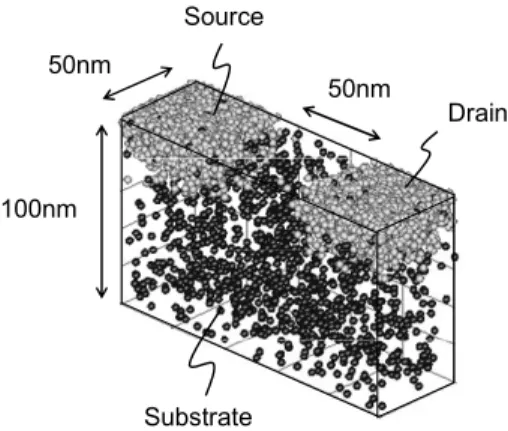
Fig. 1 Example of random dopant placement.
whose channel length and width areLandWis given by n=NS U BWDEPLW, WDEP=
2εSϕS/qNS U B, (1) whereWDEP is the depth of the depletion region below the channel inversion layer, in which the dopants are ionized,εS
is permittivity of Si, andϕS is surface band bending (∼1 V).
For example, ifL=50 nm,W=100 nm,NS U B=1018cm−3and ϕS=1 V,nis only 256.5. Assuming that the number obeys Poisson distribution, the actual number will vary around n with a standard deviation n1/2. Therefore, if we sim- ply assume thatVT H deviation caused by a single charge is q/COXLW, whereCOXis gate capacitance per area, standard deviation of threshold voltageσVT will be
σVT = √
n× q
COXLW = q COX
NS U BWDEP
LW . (2) According to a more strict derivation considering the depth dependence of the single charge impact [11], [12], (2) should be modified to
σVT = q COX
NS U BWDEP
3LW . (3)
From the derivation of these equations, the increase ofσVT
due to RDF asLW is scaled can be interpreted as follows.
The sensitivity of a FET to a charge increases in proportion to 1/LW, but at the same time, the average number of random charges decreases. Therefore,σVT increase is retarded than 1/LW, to be proportional to 1/(LW)1/2. This is in contrast to the case of RTN, as will be discussed later.
(3) can be transformed into a more convenient form for comparison with experimental data [6]. Using the text book VT Hformula
VT H=VF B+ϕS +qNS U BWDEP
CINV
, (4)
(3) becomes σVT=
q 3εOX
TINV(VT H+V0)
LW , V0≡−VF B−ϕS, (5) whereεOXis permittivity of SiO2,TINVis electrical gate ox- ide thickness (SiO2equivalent), andVF Bis flat band voltage.
V0is close to 0.1 V for conventional dual poly-Si gate FETs at room temperature.
Since (3) and (5) are obtained from analytical consid- erations where some details of RDF physics are ignored, the validity of these model equations must be confirmed. There- fore, three-dimensional (3D) Monte Carlo TCAD simula- tions were performed. That is, for a set of the design param- eters (TINV, NS U B, LandW), many MOSFETs identically designed, but microscopically different in impurity number and locations, were generated on a computer using random numbers. Uniform designed substrate doping without halo was assumed (in other words, the FETs were generated in such a manner that the average substrate doping of infinitely large number of FETs will be uniform). Then,VT H(defined by a current ofW/L×0.1μA atVDS=50 mV) for each FET was obtained by device simulation, andσVTwas calculated.
This was repeated for various combinations of the design parameters. It was confirmed that a relationship
σVT =BVT
TINV(VT H+V0)
LW (6)
actually holds, where the coefficientBVT equals 1.5(mVμm nm−1/2V−1/2). This BVT value (denoted BVT0 hereafter) is about 20% larger than expected from (5), due to some over- simplification of the analytical model.
While (6) is a semi-empirical model equation for RDF, it can be further used for analyzing and benchmarking ran- dom variations, if we take BVT as an index of variability definedby (6), rather than a given constant. Note thatBVT
can be easily calculated from (6) only if we knowσVT and basic FET design parameters. This index was successfully used to quantitatively understand the root causes of random variations [6]. That is, it was found thatBVT of PFETs from various fabs and technologies almost coincide withBVT0, if the short channel effect is properly controlled. This indi- cates that PFET random variations are dominated by RDF.
Another finding was that NFET random variations tend to be larger than expected from RDF, which suggests existence of some extra variation mechanism in NFETs that should be taken care of. Though the extra mechanism is not yet clear, it is reported that NFETBVTcan be also reduced to be com- parable to that of PFETs [13].
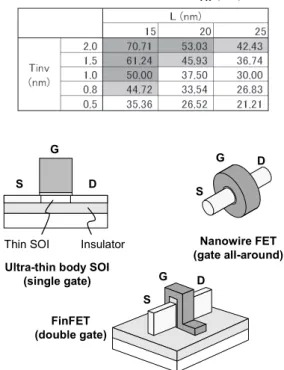
From these findings, it is now possible to estimate the scaling limit of bulk FETs set by the RDF-dominated ran- dom variations. Table 1 shows calculatedσVT, assuming that VT H +V0 = 0.5 V,W = 2L, and BVT = BVT0. It is clear that reducingTINV (thinning gate dielectric) is very ef- fective for lowering σVT. However, there should be some practical lower limit ofTINV. Considering that there is the inversion layer thickness of around 0.4 nm,TINV far below 1 nm would be difficult. ThoughσVTcan be further reduced by using retrograde channel or tweaking gate workfunction [2], the effectiveness would be limited. This is why new de- vice architectures that do not rely on substrate doping (ultra- thin body SOI FETs, FinFETs, nanowire FETs, etc. as in Fig. 2) are required to continue CMOS scaling. In these de- vices, on/offoperation of the FETs is realized by the thin or
Table 1 Estimated standard deviation ofVT H(mV) due to RDF.
Fig. 2 Examples of dopant-less body devices.
narrow body geometry, and hence, substrate doping is not necessary. A major issue associated with such dopant-less devices would be that the threshold voltage cannot be di- rectly controlled by the body doping. In some cases, the choice of availableVT Hmay be reduced.
3. Random Telegraph Noise
With the advance of CMOS scaling, random telegraph noise (RTN) has become a new reliability concern. Figure 3 shows an example of RTN waveform. The drain current of a FET switches between two discrete levels, depending on whether a trap in the gate oxide is filled by a charge or not. RTN is not something new, but rather, a special form of the ever existing low frequency noise (1/f noise) [14]. In large FETs, there are many traps that are switching as in Fig. 3, whose time constants (average time of stay in the high or low states) scatter over many decades. Superposition of such many RTN signals will result in disordered random noise.
As the FET size is reduced, the impact of a single charge (i.e. RTN amplitude here) increases similarly to the case of RDF, while the number of traps per device decreases. As a result, the chance of encountering RTN, manifesting the single charge trapping and de-trapping behavior, increases.
Due to the increased amplitude, RTN may cause malfunc- tion of digital circuits, such as SRAMs in scaled LSIs. In this section, a model for the RTN amplitude [7] will be de- scribed. Such modeling is important in two ways. Firstly, it is necessary for designing reliable circuits for state-of- the-art technologies. Secondly, it is useful for predicting the impact of the residual-charge-induced variability in fu- ture SOIFETs and FinFETs, where only limited numbers of
Fig. 3 Typical RTN waveform. Arrows show traces of superposed small amplitude RTN signal.
charges are involved.
3.1 Single Charge Response
In the previous section, only the standard deviationσVTwas discussed. Fortunately, it is reported that the random varia- tions ofVT Hare normally distributed [4], [15], thanks to the relatively large number of discrete charges in the substrate.
Assuming normal distributions, one can readily design cir- cuits if onlyσVT is known. For obtainingσVT expressions (2) and (3), only the number variation was explicitly consid- ered. For RTN, in contrast, a different modeling approach, based on single charge response, is necessary. This is be- cause the number of charges involved is very limited (may be one or a few). Normal distributions can no longer be as- sumed. Therefore, variability amplitude model starting from characteristics shift caused by adding a single charge (i.e.
single charge response) is proposed. For this purpose, sta- tistical information of single charge response is necessary, preferably obtained experimentally. This is actually possi- ble by simply measuring RTN amplitudes for many transis- tors. The measured VT H shift due to a charge is, in fact, not necessarily equal toq/CG, or any constant, and is widely varied, obeying exponential distributions in many cases [7], [8]. Because of the long tail of the exponential distributions, extremely large amplitude may accidentally occur.
The origin of this large variation in single charge re- sponse was studied, again using 3D TCAD simulations. At the Si/SiO2interface of a MOSFET (L=50 nm,W=100 nm, TINV=2.4 nm, uniform NS U B=1.5 × 1018cm−3), a single charge was placed, and the resultingVT H shift was simu- lated. This was repeated 300 times by randomly selecting the charge position in the channel plane, and theVT H shift distributions were obtained. This was done for two different cases. In one case, the discreteness of the dopants was ig- nored, and the substrate and source/drain impurity concen- trations were treated as continuous functions of position. In the second, discreteness of impurity distributions was taken
Fig. 4 Simulated probability distributions of single charge response.
Fig. 5 Top view charge positions exhibiting the largest, middle and smallest 10%VT Hshift in Fig. 4 (continuous doping case).
into account. Regarding the doping distributions, all the 300 FETs are identical in the first case, whereas all the FETs are microscopically different in the second. Figure 4 shows the simulated cumulative distribution functions (cdf) of the single charge response. An exponential distribution, consis- tent with the experimental reports, was obtained only if the discreteness of the dopants was considered.
Figure 5 shows the positions of the traps at which the VT Hshift was among the top 10%, middle 10% and bottom 10% for the case of continuous doping. It can be seen that the FETs are sensitive to a charge located on the equidistant line between the source and drain (dashed line in Fig. 5), particularly at the width-wise edge of the channel. This is because the peak of the potential barrier that a carrier must surmount to flow is located on the line, where the barrier height is most effectively modulated by a charge. The cur- rent flow tends to concentrate at the edge due to potential dips caused by electric field crowding. As a result, a charge located at the edge of the line causes the largestVT Hshift.
Though the position dependence of the device sensi- tivity as in Fig. 5 can explain part of the variation of the single charge response, VT H shift can never exceed a cer- tain upper limit if the continuous doping is assumed. The infinitely decaying tail of the exponential distributions as in Fig. 4 is explained by the so-called percolation effect caused
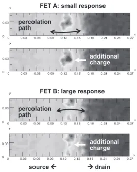
Fig. 6 Top view potential distributions with and without an additional charge in two FETs with different arrangements of impurity atoms.
by RDF. Figure 6 shows top view potential distributions in 50 nm×50 nm identically designed NFETs with two differ- ent arrangements of impurity atoms. If a negative charge is placed at the center of the channel, simulatedVT H shift was 2.7 mV in FET A, whereas 18.5 mV in FET B. This is because in FET B, a low potential current path is formed between the source and drain, which accidentally coincide with the center of the channel. Since the drain current tends to flow through this path, the additional charge effectively blocks the current, resulting in a large increase ofVT H. In FET A, since the potential is high and the current density is low at the channel center, the current change due to the charge placement is small.
3.2 Amplitude Model
Starting from the single charge response information, the statistical distributions of the noise amplitude can be straightforwardly calculated, as follows. To do this, it is assumed that the RTN amplitude is additive; i.e. if two RTN signals are superposed, the resulting waveform is simply the summation of the two. Let us denote the probability distri- bution function (pdf) for a single trap RTN amplitude (i.e.
single charge response)P1(x), wherexis a statistical vari- able such as VT H. Also denoting the maximum (peak-to- peak) amplitude pdf when exactly N traps exist in a FET PN(x), it can be easily calculated by recursive convolution ofP1(x) as
PN(x)= ∞
−∞PN−1(x−t)P1(t)dt. (7) Then, the pdf of the maximum amplitudeP(x) when the trap numberNis also random is given by
Fig. 7 CalculatedP(x) for variousλ.
P(x)=α0δ(x)+∞
i=1
αiPi(x), (8)
whereaNis the probability of havingNtraps in the FET. The delta function in the right-hand side corresponds to the cases where no trap exists in the device. A reasonable assumption here would be that the number obeys Poisson distribution
αN=exp (−λ)λN/N!, (9)
whereλis the expectation of the trap number. In a special case whenP1(x) is exponential, i.e.
P1(x)= 1 Λexp
−x Λ
(x≥0), 0 (x<0) (10) whereΛis the expectation of single charge amplitude,
PN(x)= xN−1 (N−1)!ΛN exp
−x Λ
. (11)
Figure 7 shows calculatedP(x) for variousλ, assuming (9) and (10). P(x) changes withλ, from a highly asymmetrical exponential shape towards normal distributions, according to the central limit theorem. Note that the concept of this single-charge-based modeling as described here will be use- ful not only for RTN, but also any residual-charge-induced variability.
Using this model, the dependence of RTN impact on FET scaling will be discussed. For this purpose, it is con- venient to extract a worst case amplitudexWORST, which is defined by
∞
xWORST
P(x)dx=F, (12)
whereF is an appropriate cumulative failure value (a con- stant much smaller than unity) for defining xWORST. Note that, xWORST is an indicator of the width of P(x) distribu- tions, similar to “3σ” and “6σ” used for normal distribu- tions. From the numerically calculated data as in Fig. 7, xWORST was extracted for various combinations ofλandF. Then, it was found that the following empirical equation ex- cellently reproduces the calculatedxWORST.
Fig. 8 Calculated dependence ofxWORSTon LW.
xWORST/Λ =a0+a1
√λ+λ+a2logλ, (13) wherea0,a1anda2are fitting parameters depending only on F. Further assuming the simple size dependence as already discussed for RDF
Λ =c1/LW
λ=c2LW (14)
wherec1andc2are device-dependent constants, xWORST=c1c2+a1c1√
c2
√LW +c1
a0+a2log (c2LW)
LW . (15)
The size-independent first term of the right-hand side, which equalsΛλ, roughly corresponds to the peak position ofP(x) for λ 1. If the charges are all fixed charges, instead of time-dependent traps, this term will simply cause an average shift of VT H. The second obviously corresponds to (3) in the previous section, which represents the number variation of the traps. The unique feature of (15) is the third term.
It becomes dominant when λbecomes close to or smaller than unity, or whenLW becomes small. The origin of this term is the variability of the single charge response. The contributions of these 1st, 2nd and 3rd terms on xWORST for λ=0.1 and 30 are shown in Fig. 7 by arrows.
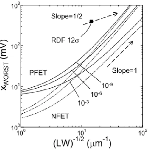
Figure 8 shows calculatedxWORST vs. 1/(LW)1/2curves.
The parameters c1 andc2 were determined from the mea- sured Λ and λ, of 55 nm SRAM cell transistors (access NFETs and load PFETs) reported in [7]. A typical 12σ value for normally distributed RDF is also plotted in the fig- ure. Note that if P(x) is a zero mean normal distribution, xWORST calculated from (12) is 6σforF=10−9. Also noting that xWORST for RTN is the spread ofP(x) in both positive and negative directions around the mean, 12σof RDF cor- responds to the RTNxWORSTforF=10−9. CalculatedxWORST
is larger in PFETs than NFETs because more traps exist in PFETs. Figure 8 shows that the worst case RTN amplitude is still much smaller than the worst case spread of RDF. How- ever, this does not mean that RTN is not important, because RTN is completely different from ordinary random varia- tions in that it is time-dependent [16]–[18]. There is a con- cern that faulty devices may erroneously pass the screening
Fig. 9 Scaling trend of RDF and residual charge fluctuation (RCF).
tests, and be shipped to the market. This can happen be- cause there are RTN traps which do not frequently switch, and cannot be detected by short time tests. To deal with this issue theoretically, it is necessary to extend the model described here to take into account the time-dependence.
Methods for designing reliable SRAMs considering the sta- tistical time-dependence of RTN are reported in [16] and [18]. It should be also noted that the relative importance of RTN as compared with RDF increases with scaling, because RTN increases faster due to the 1/LWterm in (15), as shown in Fig. 8. It is considered that this is the reason why RTN has attracted attention later than RDF.
As we continue shrinking CMOS devices, RDF in- crease of conventional bulk FETs will become unacceptable at some generation, and a dopant-less body device structure will be adopted. However, even after that, variability caused by random charges, which would be called “residual charge fluctuation (RCF)”, will remain. Figure 9 schematically shows the scaling trend of such discrete-charge-induced variability. The curves drawn are the 6σof RDF scaled in proportion to 1/(LW)1/2, and one half ofxWORST by (15) us- ing the RTN parameters for the PFETs andF=10−9, just for rough illustration of the trend of RDF and RCF. The latter curve may underestimate RCF because charges other than the detectable RTN traps [17] are ignored, or may over- estimate because the single charge response will become smaller in the dopant-less devices due to the lack of the per- colation effect. The scaling ofTINV is not considered for simplicity. Basically, RCF will rapidly increase according to (15) similarly to RTN. Therefore, even if RDF is removed, RCF will become unacceptable at some point of scaling.
Therefore, discrete-charge-induced variability will continue to be a problem, as scaling down of CMOS devices contin- ues, and eventually, will set a limit of CMOS scaling.
4. Conclusion
Random placement of discrete charges causes significant variability of scaled MOS devices. In conventional bulk FETs, RDF is the most important source of random varia-
tions. More recently, RTN has also become a new reliability concern. The magnitude of RDF can be analytically mod- eled by simply considering the number variation, whereas for RTN, statistical information of single charge response is necessary, because of the fewer number of charges involved.
Discrete-charge-induced variability will continue to be im- portant as long as scaling is continued, even after RDF is removed by switching to dopant-less device architectures.
Acknowledgement
The author would like to thank Prof. T. Hiramoto, Drs. S. Kamohara, A. Nishida, A. T. Putra, T. Tsunomura, and T. Fukai for valuable and extensive discussions about random variations, Drs. Y. Hayashi, K. Imai, S. Yokogawa, and T. Nagumo of Renesas Electronics Corp. for useful comments and support for the RTN study.
References
[1] K. Kuhn, C. Kenyon, A. Kornfeld, M. Liu, A. Maheshwari, W. Shih, S. Sivakumar, G. Taylor, P. VanDerVoorn, and K. Zawadzki, “Man- aging process variation in Intel’s 45 nm CMOS technology,” Intel Technology Journal, vol.12, pp.93–109, 2008.
[2] K. Takeuchi, A. Nishida, and T. Hiramoto, “Random fluctuations in scaled MOS devices,” Proc. SISPAD, pp.79–85, 2009.
[3] H.-S. Wong and Y. Taur, “Three-dimensional “atomistic” simulation of discrete random dopant distribution effects in sub-0.1μm MOS- FET’s,” IEDM Tech. Dig., pp.705–708, 1993.
[4] T. Mizuno, J. Okamura, and A. Toriumi, “Experimental study of threshold voltage fluctuation due to statistical variation of chan- nel dopant number in MOSFET’s,” IEEE Trans. Electron Devices, vol.41, no.11, pp.2216–2221, 1994.
[5] A. Asenov, “Random dopant induced threshold voltage lowering and fluctuations in sub-0.1μm MOSFET’s: A 3-D “atomistic” simula- tion study,” IEEE Trans. Electron Devices, vol.45, no.12, pp.2505–
2513, 1998.
[6] K. Takeuchi, T. Fukai, T. Tsunomura, A.T. Putra, A. Nishida, S. Kamohara, and T. Hiramoto, “Understanding random threshold voltage fluctuation by comparing multiple fabs and technologies,”
IEDM Tech. Dig., pp.467–470, 2007.
[7] K. Takeuchi, T. Nagumo, S. Yokogawa, K. Imai, and Y. Hayashi,
“Single-charge-based modeling of transistor characteristics fluctu- ations based on statistical measurement of RTN amplitude,” Dig.
Symp. VLSI Tech., pp.54–55, 2009.
[8] C.M. Compagnoni, R. Gusmeroli, A.S. Spinelli, A.L. Lacaita, M.
Bonanomi, and A. Visconti, “Statistical model for random telegraph noise in flash memories,” IEEE Trans. Electron Devices, vol.55, no.1, pp.388–395, 2008.
[9] T. Grasser, B. Kaczer, W. Goes, H. Reisinger, Th. Aichinger, Ph.
Hehenberger, P.-J. Wagner, F. Schanovsky, J. Franco, Ph. Roussel, and M. Nelhiebel, “Recent advances in understanding the bias tem- perature instability,” IEDM Tech. Dig., pp.82–85, 2010.
[10] V. Huard, C. Parthasarathy, C. Guerin, T. Valentin, E. Pion, M.
Mammasse, N. Planes, and L. Camus, “NBTI degradation: From transistor to SRAM arrays,” Proc. IRPS, pp.289–300, 2008.
[11] K. Takeuchi, T. Tatsumi, and A. Furukawa, “Channel engineering for the reduction of random-dopant-placement-induced threshold voltage fluctuation,” IEDM Tech. Dig., pp.841–844, 1997.
[12] P.A. Stolk, F.P. Widdershoven, and D.B. M. Klaassen, “Model- ing statistical dopant fluctuations in MOS transistors,” IEEE Trans.
Electron Devices, vol.45, no.9, pp.1960–1972, 1998.
[13] X. Yuan, et al., “Transistor mismatch properties in deep- submicrometer CMOS technologies,” IEEE Trans. Electron De-
vices, vol.58, no.2, pp.335–342, 2011.
[14] M.J. Kirton and M.J. Uren, “Noise in solid-state microstructures:
A new perspective on individual defects, interface states and low- frequency (1/f) noise,” Adv. Phys., vol.38, pp.367–468, 1989.
[15] T. Tsunomura, A. Nishida, and T. Hiramoto, “Analysis of NMOS and PMOS difference in VT variation with large-scale DMA-TEG,”
IEEE Trans. Electron Devices, vol.56, no.9, pp.2073–2080, 2009.
[16] K. Takeuchi, T. Nagumo, K. Takeda, S. Asayama, S. Yokogawa, K.
Imai, and Y. Hayashi, “Direct observation of RTN-induced SRAM failure by accelerated testing and its application to product reliability assessment,” Dig. Symp. VLSI Tech., pp.189–190, 2010.
[17] T. Nagumo, K. Takeuchi, S. Yokogawa, K. Imai, and Y. Hayashi,
“New analysis methods for comprehensive understanding of random telegraph noise,” IEDM Tech. Dig., pp.759–762, 2009.
[18] K. Takeuchi, T. Nagumo, and T. Hase, “Comprehensive SRAM design methodology for RTN reliability,” Dig. Symp. VLSI Tech., pp.130–131, 2011.
Kiyoshi Takeuchi received the B.S., M.S., and Ph.D. degrees from the University of To- kyo, Tokyo, Japan, in 1984, 1986, and 1989, respectively. Since 1989, he has been engaged in the research on high performance CMOS de- vice/circuit design, modeling, and related device physics, with NEC, NEC Electronics, and cur- rently Renesas Electronics Corporation. He was also with Semiconductor Leading Edge Tech- nologies Inc., Tsukuba, Japan to join MIRAI project from 2006 to 2011. His recent research area is device variability, reliability, and related modeling for reliable cir- cuit design.