Effects of Doping in Photovoltaic Organic
Semiconductor Films
2015
Yusuke Shinmura
Contents
Contents
Chapter 1: General Introduction 1
1.1. Background 1
1.2. Impurity Doping 2
1.2.1. Doping of Inorganic Semiconductors 2
1.2.2. Doping of Organic Semiconductors 3
1.2.3. Dopants for Organic Semiconductors 7
1.3. Carrier Concentration in Doped Semiconductors 10
1.4. Kelvin Probe Measurements 14
1.4.1. Principle of Kelvin Vibrating Capacitor Method 14
1.4.2. Determination of the Carrier Concentration 15
1.5. Donor/Acceptor Sensitization 16
1.6. Purpose of This Thesis 20
1.7. Overview of Thesis 21
1.8. References 23
Chapter 2: Experimental Equipment and Methods 28
2.1. Purification of Organic Semiconductors 28
2.2. Experimental Environment 30
2.3. Finely Controlled Doping 31
2.4. Kelvin Probe Measurements 34
2.5. Capacitance-Voltage Measurements 35
2.6. Fabrication of Organic Solar Cells 36
2.7. Measurements of Photovoltaic Properties 37
Contents
2.7.1. General 37
2.7.2. Current Density-Voltage (J-V) Characteristics 38
2.7.3. Action Spectrum 40
2.8. Conductivity Measurements 41
2.9. References 42
Chapter 3: pn-Control and pn-Homojunction Formation of Metal-free Phthalocyanine by Doping 43
3.1. Introduction 44
3.2. Experimental 45
3.3. Results and Discussion 46
3.3.1. Control of Fermi Level in a Single H2Pc Film by MoO3 and Cs2CO3 doping 46
3.3.2. Formation of p- and n-Schottky Junctions and pn-Homojunction 48
3.4. Conclusion 54
3.5. References 55
Chapter 4: Improvement of Photovoltaic Characteristics by MoO3 Doping of Thick Hole-Transporting Films 58
4.1. Introduction 59
4.2. Experimental 60
4.3. Results and Discussion 61
4.3.1. Fermi Level Shifts by Doping with MoO3 61
4.3.2. Formation of CT Complexes 62
Contents
4.3.3. Decrease in Film Resistances 64
4.3.4. Improvement of Photocarrier Generation 65
4.4. Conclusion 71
4.5.References 72
Chapter 5: Mapping of band-bending for doped C60 films 74
5.1. Introduction 75
5.2. Experimental 77
5.3. Results and Discussion 78
5.3.1. Mapping of Band-bending for Doped C60 Films 78
5.3.2. Carrier Concentration and Doping Efficiency 80
5.4. Conclusion 86
5.5. References 87
Chapter 6: Ionization Sensitization of Doping in Co-deposited Organic Semiconductor Films 90
6.1. Introduction 91
6.2. Experimental 92
6.3. Results and Discussion 93
6.3.1. Sensitization of Doping in Co-deposited Films 93
6.3.2. Mechanisms of the Sensitization 99
6.4. Conclusion 106
6.5. References 107
Contents
Chapter 7: Summary of Thesis 110
List of Publication 111
List of Supplementary Publications 112
Oral Presentations 113
Poster Presentations 115
List of Books 116
Acknowledgement 117
Chapter 1: General Introduction
1
Chapter 1:
General Introduction
1.1. Background
Impurity doping is an indispensable technique for present inorganic semiconductor devices.1) With this technique the position of the Fermi level and the conduction type of the semiconductor can be controlled. Semiconductors that have higher hole than electron concentration are described as p-type semiconductors. Conversely, semiconductors which have higher electron concentration are described as n-type semiconductors. By bringing p- and n-type semiconductors into contact with
each other various electronic devices can be created. Solar cells, which generate electrical power, operate by separating the carriers in a pn-junction.2-6) Light emitting diodes, which rely on carrier recombination in a pn-junction, can emit light of various wavelengths depending on the type of semiconductor.7-9) Bipolar field-effect transistors used as electronic switches consist of npn or pnp junctions.2)
The fabrication techniques for these devices were well established during the 20th century. These devices are widely prevalent and are an essential part of our everyday lives. Thus, impurity doping currently plays a significant role in the electronics industry.
On the other hand, organic electronic devices, i.e., devices consisting of organic semiconductors, have attracted much attention during the 21st century. Compared to inorganic semiconductors, organic semiconductors have some advantages in that the device fabrication is easy, the production costs low, and they are flexible, lightweight and easy to design.
Chapter 1: General Introduction
2
Since Inokuchi et al. reported on the high conductivity of the perylene-bromine complex in 195410), studies on organic semiconductor have advanced. However, organic semiconductors have fallen far behind inorganic semiconductors in terms of device applications. In groundbreaking work in the late 1980s, Tang reported on organic solar cells (OSCs)11) and organic light emitting diodes (OLEDs).12) While the practical use of OLEDs for display and lighting panels has been extensive, OSCs are still in the research phase. As is the case for inorganic semiconductors, further development of organic electronics requires precise pn-control in organic semiconductors. In particular, pn-control in OSCs has the potential to obtain high photo-conversion efficiencies comparable to inorganic solar cells. Thus, the author has focused on the effects of doping in organic semiconductors for solar cell application.
1.2. Impurity Doping
1.2.1. Doping of Inorganic Semiconductors
Impurity doping of inorganic semiconductors is a well-established technique. Impurities are introduced into the lattice of an inorganic semiconductor by diffusion or ion implantation. The mechanisms for doping Si are shown in Fig. 1.1. Doping Si, which has four valence electrons, with boron (B), which has three valence electrons, induces the B atom to accept an electron from Si lattice creating a hole that orbits the ionized acceptor (B-) via a weak Coulomb attraction, which can dissociate easily and move freely due to the thermal energy at room temperature (Fig. 1.1(a)). Thus, acceptor doping increases the hole concentration and changes the semiconductor to p-type. Donor doping can be described similarly (Fig. 1.1(b)). Doping with
Chapter 1: General Introduction
3
phosphorus (P), which has five valence electrons, gives an excess electron that is not required for bonding. This excess electron orbits the ionized donor (P+), but can dissociate easily and move freely. Thus, donor doping increases the electron concentration and changes the semiconductor to n-type. This pn-control gives flexibility in designing the energy structure of various electronics devices.
Fig. 1.1 Schematic illustrations of (a) p-type and (b) n-type silicon. The gray, blue and red circles indicate silicon atoms, a negatively charged boron atom and a positively charged phosphorus atom, respectively.
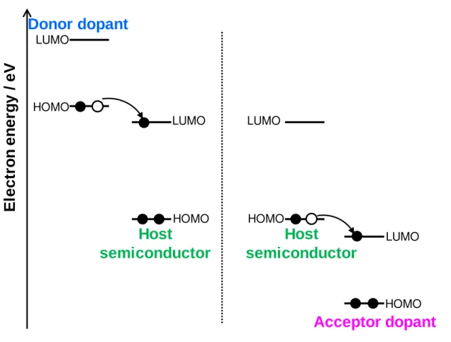
1.2.2. Doping of Organic Semiconductors
The principle of doping organic semiconductors is shown in Fig. 1.2. The highest occupied molecular orbital (HOMO) of the donor dopant needs to be located at a significantly shallow position, so that the donor dopants can supply electrons to the lowest unoccupied molecular orbital (LUMO) of the host material. In contrast, the
P+
1 nm
Si(b)
(a)
B-
Si
h+ e-
1 nm
Chapter 1: General Introduction
4
LUMO of the acceptor dopant needs to be located at a deep position, so that the acceptor dopants can extract an electron from the HOMO of the host material. Thus, charge transfer between the host semiconductor and the dopant is induced by the difference in energy levels between them.
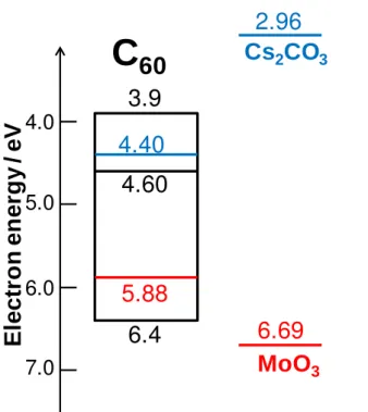
The pn-control of C60 film based on charge transfer has been reported.13-15) Fig. 1.3 shows an energy diagram of a doped C60film. The Fermi level (EF) of the C60
film doped with Cs2CO3 has shifted toward the LUMO and reached 4.40 eV compared to 4.60 eV for the undoped film, which indicates that the C60 has become n-type. On the other hand, EF in the C60 film doped with MoO3 has shifted toward the HOMO and reached 5.88 eV, indicating that the C60 has become p-type. While C60 is generally used as n-type material, doping can change the conduction type from n- to p-type. Control of the conduction type offers more flexibility in designing the energy band structure. On the other hand, metal-free phthalocyanine (H2Pc) is a typical p-type material. Whether or not it is possible to change the conduction type of H2Pc is a fascinating question. Thus, the author examined the doping of H2Pc and reports on the results in this thesis (see chapter 3).
Chapter 1: General Introduction
5
Fig. 1.2 Schematic diagrams of n-type (left) and p-type (right) doping of organic semiconductors.
LUMO
HOMO
LUMO
HOMO
Donor dopant
LUMO
HOMO LUMO
HOMO
Acceptor dopant
E le c tr on e ne rgy / eV
Host
semiconductor
Host
semiconductor
Chapter 1: General Introduction
6
Fig. 1.3 Energy diagram of doped C60. The black, red and blue lines indicate the energy levels of EF for non-doped, MoO3-doped, and Cs2CO3-doped films, respectively. The work functions of Cs2CO3 and MoO3 are also shown. The doping concentration is 3,000 ppm.
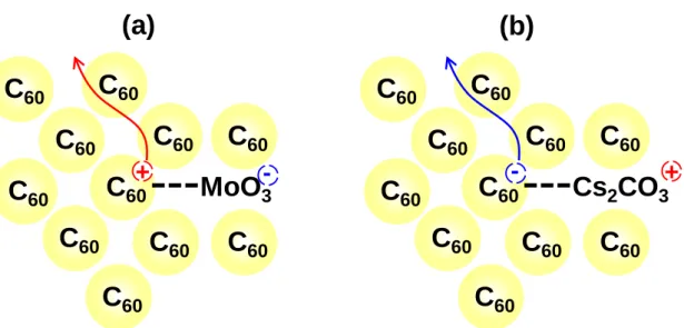
Host organic semiconductors and dopants form charge-transfer (CT) complexes. Kubo et al. described the formation of some CT complexes, i.e., C60+---MoO3-13)and C60----Cs2CO3+14,15) (Fig. 1.4). MoO3 can extract an electron from the valence band of C60 owing to its extremely high work function. In contrast, Cs2CO3 can donate an electron to the conduction band of C60 owing to its low work function. A film of C60
with mixed dopants changed color and showed CT absorption. Unlike the doping of inorganic semiconductors, dopants are not incorporated into the lattice of the host semiconductor.
4.0
5.0
6.0
7.0
3.9
6.4
C 60
5.88
4.60
4.40
6.69
2.96
Cs
2CO
3MoO
3E le c tr on e ne rgy / eV
Chapter 1: General Introduction
7
Fig. 1.4 Mechanisms of (a) MoO3 and (b) Cs2CO3 doping of C60.
1.2.3. Dopants for Organic Semiconductors
Fig. 1.5 summarizes the various donor and acceptor dopants for organic semiconductors. The introduction of halogen gases such as bromine16) and iodine17,18) into organic semiconductors for p-type doping has been performed. However, these small molecule gases diffuse easily in organic semiconductors, making precise control of the doping by halogen gases quite difficult. So, larger molecules are desirable to prevent diffusion. Some acceptor molecules have been reported. In 1960, Kearns et al. reported an increase by a factor of 107 of the dark conductivity in metal-free phthalocyanine by the addition of ortho-chloranil.19) Maitrot et al. reported a drastic
increase in conductivity by p-type doping with 2,3-dichloro-5,6-dicyano-1,4-benzoquinone (DDQ) and tetracyanoquinodimethane
(TCNQ).20) Schottky diode fabrication using DDQ doped oligothiophene has also been reported.21) The Leo group have done systematic studies using
C
60MoO
3C
60C
60C
60C
60C
60C
60C
60C
60C
60-
+
C
60C
60Cs
2CO
3C
60C
60C
60C
60C
60C
60C
60C
60C
60- +
C
60(a) (b)
Chapter 1: General Introduction
8
tetrafluoro-tetracyano-quinodimethane (F4-TCNQ) for OSCs and OLEDs.22,23) Metal oxides, i.e., molybdenum oxide (MoO3)13,14,24,25)
and vanadium oxide (V2O5),26 which have been used as hole injection layers for OLEDs are used as acceptor dopants. Antimony pentachloride (SbCl5) and iron (III) chloride (FeCl3)27) also have strong electron acceptability attributed to their high work function.
On the other hand, n-type doping is more difficult because of the instability of donor dopants with respect to oxygen. Exposure to oxygen must be prevented in order to perform n-type doping since oxygen works as an acceptor. Conventionally, alkali metals such as sodium, potassium, lithium, cesium, or strontium have been used.28-30) However, undesirable diffusion into organic films complicates precise fabrication of devices. Moreover, metal atoms work as recombination centers, which can have a considerable detrimental impact on the device characteristics. Doping with electron-donating organic molecules has also been reported. Bis(ethylenedithio)-tetrathiafulvalene (BEDT-TTF) doping of naphthalenetetracarboxylic dianhydride (NTCDA) shows an increase in conductivity and a negative EF shift.31) A UPS study of n-type doping with tetrathianaphthacene (TTN) has been reported.32) Furthermore, various other acceptor dopants such as cationic salts33-36), and transition metal complexes including Ru37), Co38,39), Cr40), and W40-42) have also been reported. Air-stable cesium carbonate (Cs2CO3),15,43-45) which is often used as an electron extracting layer,46) is one of the most appealing acceptor dopants.
In this thesis, the author used MoO3, FeCl3 and Cs2CO3 because of their strong electron acceptor and donor qualities and their ease of handling.
Chapter 1: General Introduction
9
Fig. 1.5 (a) Acceptor and (b) donor dopants for organic semiconductors. Cr2(hpp)4 CoCp2 [Ru(terpy)2]0
BEDT-TTF TTN
Halogen gases: Br2, I2 Alkali metals: K, Na, Li, Cs, Sr
F4-TCNQ
Metal oxides: MoO3, V2O5, WO3
SbCl5, FeCl3
Cs2CO3
W2(hpp)4
[Cr(bpy)3]0 Pyronin B chloride
Leuco Crystal Violet
AOB
DDQ TCNQ
ortho-chloranil
(a) (b)
Chapter 1: General Introduction
10
1.3. Carrier Concentration in Doped Semiconductors
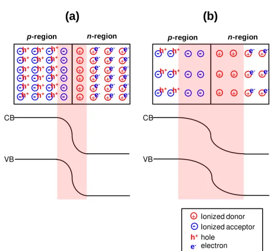
Fig. 1.6 Schematic illustrations of space charge distributions (upper) and energy band structures (bottom) in the case of (a) high and (b) low doping concentrations. The red shaded parts indicate depletion regions.
Understanding the energy structure of doped organic semiconductors is indispensable for designing devices. In particular, the depletion layer width (Wdep) is an important factor. Schematic illustrations of the space charge distributions and energy band structures in pn-junctions are shown in Fig. 1.6. With the p- and n-layers in contact, holes in the p-layer diffuse into the n-layer due to the hole density gradient. Conversely, electrons in the n-layer diffuse into the p-layer. A depletion layer is
+
+ + + + + +
+ + + + +
- - - - - -
- - - - - -
+ +
+ +
+ +
- - - - - -
+ + + + + + + + + + + + + + + + + +
- - - - - -
- - - - - -
- - - - - -
e-
e- e- e-
e- e- e-
e- e- e- e- e- e-
e- e- e- e- e- e-
e- e- e- e- e-
h+ h+
h+ h+ h+ h+
h+ h+ h+ h+ h+ h+ h+
h+ h+ h+ h+ h+ h+
h+ h+ h+ h+ h+
p-region n-region p-region n-region
CB
VB CB
VB
(a) (b)
+
e- - h+
Ionized donor Ionized acceptor hole
electron
Chapter 1: General Introduction
11
(1.2)
(1.3) formed by recombination of the diffused holes and electrons at the interface between the p- and n-layers. Wdep is determined by the carrier concentration. In the case of high doping concentration, the change in potential at the pn-junction is large due to the combination of a large number of electrons and holes (Fig.1.6(a)). The large electric field formed in a narrow region limits the spread of Wdep. Conversely, Wdep spreads widely in the case of low carrier concentration (Fig.1.6(b)). That is, as the doping concentration increases, Wdep becomes narrower. Thus, there is a close relationship between Wdep and carrier concentration. The relationship can be found using Poisson’s equation.2) The electrostatic potential (Ψ) is obtained from Poisson’s equation,
d2Ψ dx2 ≡ −
dE dx= −
ρs
εε0 = − e
εε0(ND− NA+ p− n)
where, ρs, ε, ε0, ND, NA, p and n are the resistivity and relative permittivity of the semiconductor, the permittivity in vacuum, and the donor, acceptor, free hole and free electron concentrations, respectively.
Since there are no carriers in the depletion region, i.e., p=n=0, this equation reduces to d2Ψ
dx2 = e
εε0(ND− NA)
The space charge distribution for an abrupt junction is shown in Fig. 1.7. Poisson’s equation can be simply expressed as,
d2Ψ dx2 =
eNA
εε0 (−xp≤ x < 0) d2Ψ
dx2 = eND
εε0 (0 <� ≤ xn)
Since the space charge of whole semiconductor is neutral, the negative charge in the p-region must equal the positive charge in the n-region. Thus,
NAxp=NDxn (1.4)
Chapter 1: General Introduction
12
(1.6) where, xp and xn are the widths of the depletion layer in the p- and n-regions, respectively.
The electric field intensity is obtained by integration of Eq. (1.3), E(x) = dΨ
dx =
eNA(x + xp)
εε0
(−xp ≤ x < 0) E(x) = eND(x− xn)
εε0 (0 <� ≤ xn)
Integration of the electric field given by Eq (1.5) gives the built-in potential (Vbi). Thus, the area of the triangle in Fig. 1.7(b) indicates Vbi.
V(x) =−eND 2εε0xp
2+eND
εε0 xn 2 =1
2EmWdep
Fig. 1.7 (a) Space charge distribution in the depletion region in thermal equilibrium. (b) Electric field distribution of a pn-junction. The area of the red shaded triangle corresponds to Vbi.
Depletion region (Wdep)
N
D-N
A0 x
n x-x
px
(a)
(b) 0
E
-E
mp-type region n-type region ND-NA
(1.5)
Chapter 1: General Introduction
13
From Eq. (1.4) and (1.6), Wdep is obtained as a function of Vbi.
Wdep = �2εε0 e �
NA+ ND NAND � Vbi
A junction in which the carrier concentration on one side is much higher than that on the other is called a one-sided abrupt junction. In the case of a heavily-concentrated p/low-concentrated n (p+n) junction, that is, NA>>ND, Wdep in the p-region is extremely narrow. Thus, Wdep in the n-region can simply be expressed as follows.
Wdep ≅ xn =�2εε0Vbi eND
Conversely, Wdep in the p-region in the case of an n+p junction is expressed as
Wdep ≅ xp =�2εε0Vbi eNA
Wdep of Schottky junctions can also be represented by Eqs. (1.8) and (1.9). Since Wdep and Vbi can be determined by band-mapping using a Kelvin probe, the carrier concentration can be calculated using these equations.
(1.7)
(1.8)
(1.9)
Chapter 1: General Introduction
14
1.4. Kelvin Probe Measurement
1.4.1. Principle of Kelvin Vibrating Capacitor Method
The EF in organic semiconductor films was determined using a Kelvin probe.47-55) Figure 1.8 shows the mechanism of the Kelvin vibrating capacitor method. An organic semiconductor film facing a standard gold plate probe forms a capacitor due to the difference in work function. Varying the distance between them by vibrating the gold plate generates an alternating current (AC). The voltage at which the AC is cancelled corresponds to the contact potential difference (CPD). The EF of the sample films can be determined from the difference in CPD between the sample and a standard gold plate, the work function of which has been measured by atmospheric photoelectron spectroscopy.
Fig. 1.8. the mechanism of Kelvin vibrating capacitor method
+
+
+
+
-
-
-
-
Gold plate
Capacitance
Sample
Ammeter V
E
Vibration
Chapter 1: General Introduction
15
Studies on the energy structure of organic semiconductors have been performed not only by using a Kelvin probe but also by ultra-violet photoelectron spectroscopy (UPS), X-ray photoemission spectroscopy (XPS) and inverse photoelectron spectroscopy (IPES).56-66) Using these measurements to understand the energy structure is crucial for designing devices and improving the photovoltaic characteristics.
1.4.2. Determination of Carrier Concentration
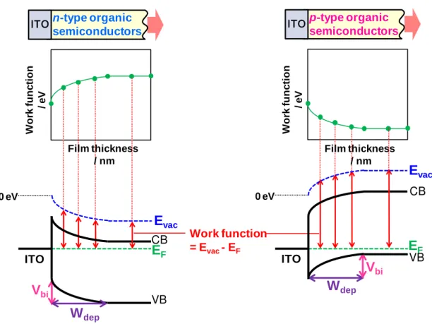
Band-mapping was performed by ascertaining the film thickness-dependence of the Fermi level measurements.45,67,68) Figure 1.9 shows the principle of band-mapping of doped organic semiconductors. When a doped organic semiconductor is in contact with an indium tin oxide (ITO) electrode, their EFs are aligned. Accordingly, the vacuum level (EVAC) is bent and the value of the work function, which is defined as the difference between EVAC and EF (Fig. 1.9, red double-headed arrows), changes with the thickness of the film. Thus, the variation in band-bending with the thickness of the doped organic semiconductor film can be directly mapped by measuring the work function with a Kelvin probe. The band-bending gives the depletion layer width (Wdep) and the built-in potential (Vbi). The carrier concentration (N) can be calculated using Eqs. (1.8) and (1.9). Furthermore, the doping efficiency, i.e., the ratio of the number of generated carriers to the amount of doped impurity can be determined.
Chapter 1: General Introduction
16
Fig. 1.9 Principle of energy band mapping of n-type (left) and p-type (right) Schottky junctions. CB and VB denote the conduction and valence bands, respectively.
1.5. Donor/Acceptor Sensitization
Organic solar cells have been substantially developed in the last decade.69-71) Since the pioneering work of Tang11) in 1986, the photo-conversion efficiency of organic solar cells has gradually increased up to 12%,72) which is comparable to amorphous silicon. Donor (D)/Acceptor (A) sensitization has been crucial for this development. In order to obtain a photocurrent, the following process is a fundamental requirement; excitons generated by the absorption of light dissociate into free electrons and holes, which then move to the electrodes by carrier transport. That is, the efficient
CB
Vbi
0 eV Work function / eV
Film thickness / nm
ITO ITO
Work function
= Evac- EF
VB
Evac
Wdep
EF
CB
Vbi
0 eV Work function / eV
Film thickness / nm
ITO
ITOp-type organic semiconductors
VB
Evac
Wdep
EF
n-type organic semiconductors
Chapter 1: General Introduction
17
dissociation of excitons is absolutely vital for generating large photocurrents. However, it is difficult to dissociate excitons in a single organic semiconductor due to the strong attractive forces. The force acting on the positive and negative charges of the exciton (F) are represented by Coulomb’s Law (Eq. (1.10)),
F =
14���0
�1�2
�2 (1.10)
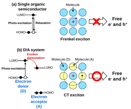
where ε, ε0, r, and q are the relative dielectric constant, the dielectric constant in a vacuum, the distance between the charges, and the magnitudes of the charges, respectively. Inorganic semiconductors have relatively large ε (>10). Thus, weakly bound Wannier excitons are formed, which can easily separate into free carriers (Fig. 1.10 (left)). On the other hand, organic semiconductors have relatively small ε (~4).73,74) Thus, strongly bound Frenkel excitons are formed, which cannot separate into free carriers (Fig. 1.10 (right)). In order to solve this problem, a device structure in which two organic semiconductor materials are in contact is required for OSCs. Electrons excited by light irradiation of a single molecule film relax before dissociation (Fig. 1.11(a)). On the other hand, a combination of a donor molecule (D) and an acceptor molecule (A) can separate the positive and negative charges to the highest occupied molecular orbital (HOMO) of D and the lowest unoccupied molecular orbital (LUMO) of A, respectively (Fig. 1.11(b)). The separated charges form a CT exciton which can dissociate easily. Thus, this D/A system is essential if a large photocurrent is to be obtained.
Chapter 1: General Introduction
18
Fig. 1.10 Schematic illustrations of (a) Wannier exciton generated in Si. (b) Frenkel exciton generated in C60.
Fig. 1.11 Schematic energy diagrams and models of photo-generated excitons in (a) single organic semiconductor and (b) D/A system.
-
+Inorganic semiconductor Si (ε=11.9)
Exciton Diameter: 9.0 nm
(a) Organic semiconductor
C60(ε=4.4)
Exciton Diameter: 0.50 nm (b)
+
-
1 nm
LUMO
HOMO
LUMO
HOMO
Electron acceptor
(A) Electron
donor (D)
Relaxation Photo-excitation
LUMO
HOMO
Photo-excitation
(a) Single organic semiconductor
(b) D/A system
Exciton
dissociation Molecule (D) Molecule (A)
+ -
CT exciton
+ -
Frenkel exciton Molecule
Free e-and h+
Free e-and h+
Chapter 1: General Introduction
19
Fig. 1.12. Schematic illustration of co-deposited film.
In order to dissociate all the excitons, a co-deposited film, i.e., a mixed film with donor and acceptor molecules such that there are D/A interfaces throughout the film, is necessary, (Fig. 1.12).75-77) In order to generate a large number of free carriers the total area of the D/A interfaces must be large. Furthermore, a thick film is needed in order to absorb all of the incoming light. However, thick organic semiconductor films generally have extremely high resistance, so, reducing the resistance by doping is necessary. Doping co-deposited films is a new approach. Only a few studies on doping to photoactive layer have been reported. Ishiyama et al. successfully performed the formation of pn-homojunctions in a co-deposited film consisting of C60 and α-sexithiophene (6T).43,44,78) Kubo et al. achieved operation of thick photovoltaic cells incorporating a doped co-deposited film consisting of C60 and H2Pc.79) Doping co-deposited films has the potential for realizing high efficiency photovoltaic cells. Thus, the author investigated the effects of doping on co-deposited films (see Chapter 6).
electrode electrode
+
-
+
- -
+
+
-
Photoactive regionChapter 1: General Introduction
20
1.6. Purpose of This Thesis
Impurity doping to control the pn-junction characteristics is vital in order to improve the photoconversion efficiency in organic solar cells as well as in inorganic solar cells. While pn-control of the typical inherently n-type C60 has been reported previously, it hasn’t been shown whether or not the same control can be achieved in the typical inherently p-type metal-free phthalocyanine (H2Pc) and hole transport materials (HTMs). The author has attempted to confirm whether or not this pn-control can be applied to any organic semiconductor in order to design high-efficiency organic solar cells. Thus, an investigation of the effects of doping on H2Pc and HTMs was performed.
Moreover, precise device design requires a quantitative evaluation of the carrier concentration in doped organic semiconductors. However, correlation between the carrier concentration and the doping concentration hasn’t so far been clarified. In particular, there have scarcely been any reports of studies on the doping of co-deposited films with photoactive D/A interfaces. The author believes that doping of co-deposited films is a key issue for the development of organic solar cells. Thus, in this thesis, the author has attempted to quantify the carrier concentration in doped single and co-deposited organic semiconductor films.
Chapter 1: General Introduction
21
1.7. Overview of This Thesis
The effects of doping on typical single semiconductors are clarified.
In chapter 3, control of the conduction type and the formation of pn-homojunctions in single H2Pc films by intentionally doping with cesium carbonate (Cs2CO3) and MoO3 is described, even though H2Pc is conventionally regarded as being inherently p-type.
In chapter 4, observations showing improvements made in the photovoltaic characteristics by p-type doping of hole-transport materials (HTMs), which offer high open-circuit voltages, are reported. Observation of strong charge transfer (CT) absorption by heavily MoO3 doped HTMs revealed the formation of CT complexes. MoO3-doping of HTMs offered the formation of built-in potentials and a decrease in resistance.
Evaluation of the carrier concentration and energy band structure of doped organic semiconductors is absolutely necessary for precise device fabrication. Thus, carrier concentration of single and co-deposited films was investigated.
In chapter 5, band-mapping of doped C60 is demonstrated using a Kelvin probe. The carrier concentrations in C60 films doped with Cs2CO3 and MoO3 were precisely determined. An ionization efficiency of 10% is suggested, which is significantly less than that for Si. The CT complex formed, i.e., Cs2CO3+–C60, is essentially the same as for the CT exciton. It is assumed that this low ionization efficiency is due to the strong attractive force between the small electron orbital and the positively ionized donor.
In chapter 6, the ionization sensitization of the dopants is revealed using measurements of the carrier concentration in a co-deposited film. H2Pc:C60
co-deposited films show a significantly higher ionization efficiency of 97%, which is
Chapter 1: General Introduction
22
comparable to doped silicon. Ionization sensitization was observed with both p- and n-type doping. A charge separation superlattice model that gives a reasonable
explanation of this phenomenon is proposed. Charge separation in a co-deposited film accelerates the liberation of the carriers from the impurity levels. The ionization sensitization is a new knowledge which gives meaning to doping of co-deposited films, and is a unique characteristic of organic semiconductors.
Chapter 1: General Introduction
23
1.8. References
1) S. M. Sze, SEMICONDUCTOR DEVICES, Physics and Technology (Wiley, New York, 1985).
2) S. M. Sze, Physics of Semiconductor Devices (Wiley, New York, 1969). 3) W. E. Spear, and P. E. Lecomber, Solid State Commun., 17, 1193 (1975).
4) M. A. Green, Silicon Solar Cells: Advanced Principles and Practice (Bridge Printery, Sydney, 1995).
5) M. S. Green, “Solar Cells” in S. M. Sze, Ed., Modern Semiconductor Device Physics, (Wiley Interscience, New York, 1998).
6) M. Yamaguchi, T. Takamoto, K. Araki, Sol. Energy. Mater. Sol. Cells, 90, 3068 (2006).
7) W. O. Groves, A. H. Herzog, and M. G. Craford, Appl. Phys. Lett., 19, 184 (1971). 8) A. A. Bergh and P. J. Dean, Light Emitting Diodes (Clarendon, Oxford, 1976). 9) S. Nakamura and G. Fasol, The Blue Laser Diode (Wiley, New York, 1977). 10) H. Akamatu, H. Inokuchi, and Y. Matsunaga, Nature, 173, 168 (1954). 11) C. W. Tang, Appl. Phys. Lett., 48, 183 (1986).
12) C. W. Tang, S.A. VanSlyke, Appl. Phys. Lett., 51, 913 (1987).
13) M. Kubo, K. Iketaki, T. Kaji, and M. Hiramoto, Appl. Phys. Lett., 98, 073311 (2011).
14) M. Kubo, T. Kaji, and M. Hiramoto, AIP Adv., 1, 032177 (2011).
15) M. Hiramoto, M. Kubo, Y. Shinmura, N. Ishiyama, T. Kaji, K. Sakai, T. Ohno, and M. Izaki, Electronics, 3, 351 (2014).
16) M. Hiramoto, K. Ihara, H. Fukusumi, and M. Yokoyama, J. Appl. Phys., 78, 7153 (1995).
Chapter 1: General Introduction
24
17) G. D. Sharma, S. G. Sangodkar, and M. S. Roy, Mater. Sci. Eng. B, 41, 222 (1996).
18) A. C. Varghese, C. S. Menon, J. Mater. Sci., 41, 3521 (2006).
19) D. R. Kearns, G. Tollin, and M. Calvin, J. Chem. Phys., 32, 1020 (1960).
20) M. Maitrot, G. Guillaud, and B. Boudjema, J. J. André, and J. Simon, J. Appl. Phys., 60, 2396 (1986).
21) E. J. Lous, P. W. M. Blom, L. W. Molenkamp, and D. M. de Leeuw, Phys. Rev. B, 51, 17251 (1995).
22) J.Blochwitz, M. Pfeiffer, T. Fritz, and K. Leo, Appl. Phys. Lett., 73, 729 (1998). 23) K. Walzer, B. Maennig, M. Pfeiffer, and K. Leo, Chem. Rev., 107, 1233 (2007) and
references therein.
24) M. Kröger, S. Hamwi, J. Meyer, T. Riedl, W. Kowalsky, and A. Kahn, Org. Electron., 10, 932 (2009).
25) M. Kubo, Y. Shinmura, N. Ishiyama, T. Kaji, and M. Hiramoto, Appl. Phys. Express, 5, 092302 (2012).
26) M. Kubo, Y. Shinmura, N. Ishiyama, T. Kaji, and M. Hiramoto, Mol. Crsyt. Liq. Cryst., 581, 13 (2013).
27) C. Ganzorig, and M. Fujihira, Appl. Phys. Lett., 77, 4211 (2000).
28) D. Ivory, G. Miller, J. Sowa, L. Shacklette, R. Chance, and R. Baughman, J. Chem. Phys., 71, 1506 (1979).
29) G. Parthasarathy, C. Shen, A. Kahn, and S. R. Forrest, J. Appl. Phys., 89, 4986 (2001).
30) J. Kido, and T. Matsumoto, Appl. Phys. Lett., 73, 2866 (1998).
31) A. Nollau, M. Pfeiffer, T. Fritz, and Karl Leo, J. Appl. Phys., 87, 4340 (2000).
32) S. Tanaka, K. Kanai, E. Kawanabe, T. Iwahashi, T. Nishi, Y. Ouchi, and K. Seki, Jpn.
Chapter 1: General Introduction
25
J. Appl. Phys., 44, 3760 (2005).
33) A. G. Werner, F. Li, K. Harada, M. Pfeiffer, T. Fritz, and K. Leo, Appl. Phys. Lett., 82, 4495 (2003).
34) A. Werner, F. Li, K. Harada, M. Pfeiffer, T. Fritz, and K. Leo, Adv. Funct. Mater., 14, 255 (2004).
35) F. Li, A. Werner, M. Pfeiffer, K. Leo, and X. Liu, J. Phys. Chem. B, 108, 17076 (2004).
36) F. Li, M. Pfeiffer, A Werner, K. Harada, K. Leo, N. Hayashi, K. Seki, X. Liu, and X. D. Dang, J. Appl. Phys., 100, 023716 (2006).
37) C. J. Bloom, C. M. Elliott, P. G. Schroeder, C. B. France, and B. A. Parkinson, J. Phys. Chem. B, 107, 2933 (2003).
38) C. K. Chan, F. Amy, Q. Zhang, S. Barlow, S. Marder, and A. Kahn, Chem. Phys. Lett., 431, 67 (2006).
39) C.K. Chan, W. Zhao, A. Kahn, and I. G. Hill, Appl. Phys. Lett., 94, 203306 (2009). 40) T. Menke, D. Ray, J. Meiss, K. Leo, and M. Riede, Appl. Phys. Lett., 100, 093304
(2012).
41) M. L. Tietze, F. Wölzl, T. Menke, A. Fischer, M. Riede, K. Leo, and B. Lüssem, Phys. Status Solidi A, 210, 2188 (2013).
42) S. Schubert, Y. H. Kim, T. Menke, A. Fischer, R.Timmreck, L. Müller-Meskamp, and K. Leo, Sol. Energy Mater. Sol. Cells, 118, 165 (2013).
43) N. Ishiyama, M. Kubo, T. Kaji, and M. Hiramoto, Appl. Phys. Lett., 101, 233303 (2012).
44) N. Ishiyama, T. Yoshioka, T. Kaji, and M. Hiramoto, Appl. Phys. Express, 6, 012301 (2013).
Chapter 1: General Introduction
26
45) N. Ishiyama, M. Kubo, T. Kaji, and M. Hiramoto, Org. Electron., 14, 1793 (2013). 46) H. Liao, L. Chen, Z. Xu, G. Li, and Y. Yang, Appl. Phys. Lett., 92, 173303 (2008). 47) M. Kotani and H. Akamatu, Bull. Chem. Soc. Jpn., 43, 30 (1970).
48) M. Kotani and H. Akamatu, Discuss. Faraday Soc., 51, 94 (1971).
49) S. Saito, T. Soumura, and T. Maeda, J. Vac. Sci. Technol. A, 2, 1389 (1984). 50) M. Iwamoto, A. Fukuda, and E. Itoh, J. Appl. Phys., 75, 1607 (1994).
51) M. Hiramoto, K. Ihara, and M. Yokoyama, Jpn. J. Appl. Phys., 34, 3803 (1995). 52) M. Pfeiffer, K. Leo, and N. Karl, J. Appl. Phys., 80, 6880 (1996).
53) Y. Harima, K. Yamashita, H. Ishii, and K. Seki, Thin Solid Films, 366, 237 (2000). 54) E. Moons, A. Goossens, and T. Savenije, J. Phys. Chem. B, 101, 8492 (1997). 55) N. Hayashi, H. Ishii, Y. Ouchi, and K. Seki, J. Appl. Phys., 92, 3784 (2002). 56) I. G. Hill and A. Kahn, J. Appl. Phys., 84, 5583 (1998).
57) R. Schlaf, B. A. Parkinson, P. A. Lee, K. W. Nebesny, and N. R. Armstrong, Appl. Phys. Lett., 73, 1026 (1998).
58) S. T. Lee, X. Y. Hou, M. G. Mason, and C. W. Tang, Appl. Phys. Lett., 72, 1593 (1998).
59) H. Ishii, K. Sugiyama, E. Ito, and K. Seki, Adv. Mater., 11, 605 (1999).
60) J. Blochwitz, T. Fritz, M. Pfeiffer, K. Leo, D.M. Alloway, P.A. Lee, and N.R. Armstrong, Org. Electron., 2, 97 (2001).
61) W. Gao and Kahn, Appl. Phys. Lett., 79, 4040 (2001). 62) W. Gao, and A. Kahn, Org. Electron., 3, 53 (2002). 63) W. Gao and A. Kahn, Appl. Phys. Lett., 82, 4815 (2003).
64) C. Chan, W. Gao, and A. Kahn, J. Vac. Sci. Technol. A, 22, 1488 (2004). 65) W. Zhao and A. Kahn, J. Appl. Phys., 105, 123711 (2009).
Chapter 1: General Introduction
27
66) W. Han, H. Yoshida, N. Ueno, and S. Kera, Appl. Phys. Lett., 103, 123303 (2013). 67) H. Ishii, N. Hayashi, E. Ito, Y. Washizu, K. Sugi, Y. Kimura, M. Niwano, Y. Ouchi,
and K. Seki, Phys. Stat. Sol. (a), 201, 1075 (2004).
68) S. Hamwi, J. Meyer, T. Winkler, T. Riedl, and W. Kowalsky, Appl. Phys. Lett., 94, 253307 (2009).
69) Y. Lin, Y. Li, and X. Zhan, Chem. Soc. Rev., 41, 4245 (2012).
70) H. Spanggaard and F. C. Krebs, Sol. Energy Mater. Sol. Cells, 83, 125 (2004). 71) H. Hoppe and N. S. Sariciftci, J. Mater. Res., 19, 1924 (2004).
72) The efficiency chart published by National Renewable Energy Laboratory (NREL). 73) M. A. Abkowitz and A. I. Lakatos, J. Chem. Phys., 57, 5033 (1972).
74) A. F. Hebard, R. C. Hadon, R. M. Fleming, and A. R. Kortan, Appl. Phys. Lett., 59, 2109 (1991).
75) M. Hiramoto, H. Fujiwara, and M. Yokoyama, Appl. Phys. Lett., 58, 1062 (1991). 76) M. Hiramoto, H. Fujiwara, and M. Yokoyama, J. Appl. Phys., 72, 3781 (1992). 77) G. Yu, J. Gao, J. C. Hummelen, F. Wudl, and A. J. Heeger, Science, 270, 1789
(1995).
78) N. Ishiyama, M. Kubo, T. Kaji, and M. Hiramoto, Appl. Phys. Lett., 99, 133301 (2011).
79) M. Kubo, T. Kaji, and M. Hiramoto, Appl. Phys. Lett., 103, 263303 (2013).
Chapter 2: Experimental Equipment and Methods
28
Chapter 2:
Experimental Equipment and Methods
2.1. Purification of Organic Semiconductors
C60 (Frontier Carbon Co., Ltd., nanom purple TL), C70 (Frontier Carbon Co., Ltd., nanom orange STH), metal-free phthalocyanine (H2Pc) (Dainippon Ink & Chemicals, Inc., Fastogen Blue EP-101), and N,N’-dimethyl-3,4,9,10-perylene tetracarboxylic diimide (Me-PTC) were purified to 7N (99.99999%) purity by temperature gradient sublimation in a quartz furnace comprising three sections at different temperatures (Fig. 2.1).1,2) Crude samples of the organic semiconductors, each weighing 4g, were placed in the high temperature section, and highly purified millimeter-scale single crystals were grown by sublimation in the middle temperature section under N2 flow after pre-heating. (Fig. 2.2). Impurities from the crude sample were expelled to the low temperature section. In order to obtain highly purified single crystals, the proper conditions with respect to each material are required. The detailed sublimation conditions are shown in Table 2.1. The hole transport material and donor dopant, cesium carbonate (Cs2CO3; Aldrich, 99.995%), and the acceptor dopants, molybdenum trioxide (MoO3; Alfa Aeser, 99.9995%) and iron (III) chloride (FeCl3; Aldrich, 99.99%), were used without further purification.
Chapter 2: Experimental Equipment and Methods
29
Fig. 2.1 Quartz furnace for growing highly purified single crystals of organic semiconductor.
Fig. 2.2 Purified single crystals of organic semiconductors and their chemical structures.
Middle High
Low
N
2flow
Crude sample
Single crystal
Impurities
C
605 mm
C
70H
2Pc Me-PTC
5 mm
Chapter 2: Experimental Equipment and Methods
30
Table 2.1 Sublimation conditions for the organic semiconductors Temperature / °C N2 flow
Pressure / atm
Heating Time / h
Low Middle High
Pre-heating 150 150 150 Under
vacuum 1
C60 310 580 745 1 36
C70 365 635 800 1 36
H2Pc 270 290 480 0.1 5
Me-PTC 270 300 500 0.1 5
2.2. Experimental Environment
The semiconductors were evaporated in an oil-free vacuum evaporation chamber (EpiTech Inc., ET300-6EHK) built into a glove box (UNICO, UL-1400ATW) (H2O < 0.7 ppm, O2 < 0.2 ppm) (Fig.2.3). The samples were not exposed to air at any time during either film fabrication or measurement in order to avoid effects due to moisture and oxygen.
Chapter 2: Experimental Equipment and Methods
31
Fig.2.3 Vacuum chamber contained within a glove box.
2.3. Finely Controlled Doping
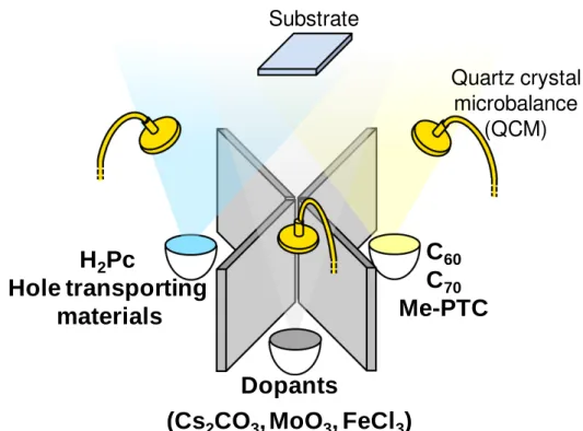
Doping of the organic semiconductors was performed by co-evaporation. Each material was put into individual Al2O3 melting pots. Evaporation was performed by resistance heating with a tungsten basket in vacuo. Evaporation rates of organic semiconductors and dopants were independently monitored by quartz crystal microbalances (QCMs) (Fig. 2.4).
Fine control of the deposition rate of small amounts of doping was performed using the QCM equipped with a computer monitoring system (ULVAC, Depoview).
Vacuum chamber
Chapter 2: Experimental Equipment and Methods
32
The film thickness monitored by the QCM was calibrated using a surface profilometer (Dektak) (Fig. 2.5). The dependence of the film thickness of the dopant on evaporation time is shown in Fig. 2.6. The evaporation rate can be determined from the gradient of the baseline (Fig. 2.6, red line). The fluctuations observed in the measurement are attributed to temperature fluctuations in the cooling water flowing through the QCM. An evaporation rate of 10-5 nm s-1 can be estimated from the gradient. When the host organic semiconductor evaporates at 0.2 nm s-1, the ratio of the evaporation rate of the dopant to that of the host organic semiconductor gives a doping concentration of 50 ppm in volume. The deposition rate for the organic semiconductors was kept to 0.2 nm s-1 and those of the dopants were adjusted from 10-5 to 2 x 10⁻³ nm s-1 to give doping concentrations from 50 to 10,000 ppm.
Fig. 2.4 Schematic illustration of coevaporation for doping of organic semiconductors. Substrate
H
2Pc
Hole transporting
materials
C
60C
70Me-PTC
Dopants
(Cs
2CO
3, MoO
3, FeCl
3)
Quartz crystal microbalance
(QCM)
Chapter 2: Experimental Equipment and Methods
33
Fig. 2.5 Stylus surface profilometer for calibrating the film thickness.
Fig. 2.6 Monitored dopant thickness vs. evaporation time.
sample
probe
0
0.02
0.04
0.06
0.08
0.1
0.12
0.14
0 1000 2000 3000 4000
Cs
2CO
3th ick n e s s / n m
Time / s
10 -5 nm/s
Evaporation time / s
Dopa nt thi c k ne s s / nm
Chapter 2: Experimental Equipment and Methods
34
2.4. Kelvin Probe Measurements
The Fermi levels (EF) in the organic semiconductor films were determined using a Kelvin probe (Riken Keiki, FAC-1) (Fig.2.7).3-11) The films were deposited on indium tin oxide (ITO) substrates. A gold plate, the work function of which was measured by atmospheric photoelectron spectroscopy, was used as a standard for the work function measurements. All EF measurements were performed in a N2
atmosphere to avoid the effects of oxygen and moisture.
Fig. 2.7 Kelvin Probe for Fermi level measurements.
Gold plate probe
Organic semiconductor film
on ITO substrate
Chapter 2: Experimental Equipment and Methods
35
2.5. Capacitance-Voltage Measurements
Capacitance–voltage (C–V) measurements were performed in order to obtain the carrier concentration (N) of doped C60 using Schottky junction cells comprising ITO/MoO3 (10 nm)/MoO3-doped C60 (1 μm)/bathocuproin (BCP) (15 nm)/Ag (100 nm).12,13) A periodic triangular bias from a function generator (Hokuto Denko HB-102) was applied to the cell and the dark current hysteresis (Fig. 2.8(a)) was measured using a picoammeter (Keithley 485).
The differential capacitance, Cd (V) was calculated using Eq. (2.1),
Cd (V) = ∆I (V)/8V0f (2.1) where ∆I (V), V0, and f are the difference in the dark current due to hysteresis, the amplitude of the scanning voltage, and the frequency of the periodic triangular bias, respectively. Mott-Schottky plots, i.e., Cd-2 vs. V plots are shown in Fig. 2.8(b). Cd-2 is given by Eq. (2.2)
Cd-2 = 2(V-Vbi)/eNε0ε. (2.2) The carrier concentration (N) can be determined from the gradient (2/eNε0ε) of the linear part (broken line).
Chapter 2: Experimental Equipment and Methods
36
Fig. 2.8 Examples of (a) dark current hysteresis and (b) a Mott-schottky plot.
2.6. Fabrication of Organic Solar Cells
Indium tin oxide (ITO) coated glass substrates (Sanyo Vacuum Industries) were washed three times with water (10 min), methanol (10 min), and acetone (10 min), respectively, in an ultrasonic bath. All of the films were deposited by vacuum evaporation onto ITO glass substrates at 10-5 Pa using an oil-free vacuum evaporator (EpiTech Inc., ET300-6E-HK). The film thicknesses were determined by simultaneous monitoring of the deposition using quartz crystal microbalances (QCM). For doping co-deposited films, the organic semiconductors and dopants were
-1.5 -1 -0.5 0 0.5 1 1.5
C
d-2/ F
-2c m
4Voltage / V
-1.5 -1 -0.5 0 0.5 1 1.5
Cur re n t / µ A
Voltage / V
0.05
-0.05
-0.1
(b)
(a)
∆ I
2V
05
10
15 × 10
14
Gradient; 2/eN ε
0ε
V
biChapter 2: Experimental Equipment and Methods
37
evaporated from different sources. Ag electrodes were deposited on the organic films through a metal mask with an aperture of 0.06 cm2.
2.7. Measurements of Photovoltaic Properties
2.7.1. General
The photovoltaic properties of the cells were measured by setting the cells in a vacuum sample container with a quartz glass window (Epi Tech Inc.) (Fig. 2.9). The container was evacuated to 10-3 Pa. The area of the photo-irradiated cell was precisely defined using a metal mask with an aperture of 0.04 cm2.
Fig. 2.9 Vacuum sample container with a quartz glass window.
Quartz glass window
To a vacuum pump
Electrical conecting ports
Organic solar cell
with metal mask
Chapter 2: Experimental Equipment and Methods
38
2.7.2. Current Density-Voltage (J-V) Characteristics
The current density-voltage (J-V) characteristics were measured by irradiating the cell with simulated solar light (USHIO INC., MS110AAA) (AM1.5, 100 mW cm-2) (Fig. 2.10). Fig. 2.11 shows typical current-voltage (J-V) characteristics in the dark and under irradiation with the simulated solar light. The voltage was swept from -1.0 to 1.0 V at 0.1 V·s-1. The photocurrent density at 0 V and the voltage at 0 mAcm-2 are defined as the short-circuit current density (Jsc) and the open-circuit voltage (Voc), respectively. The power conversion efficiency (ηp), i.e., the ratio of the maximum power that the cell can produce (Pmax) to the incident light intensity (Pin), is given by the following equation (Eq.2.3).
�
P=
PPmaxin
=
Jsc·Voc·FF
Pin
(2.3)
The fill factor (FF) is the ratio of the maximum power (red shaded rectangle, Fig. 2.11) to the product of Jsc and Voc (dashed line rectangle, Fig. 2.10) (Eq. 2.4).
FF =
�max�sc·�oc
=
�max·�max
�sc·�oc (2.4)
Jmax and Vmax are the current density and voltage at the maximum power output. FF signifies how close the J-V curve is to a step function. The closer the curve is to a step function, the larger the power that can be extracted.
Chapter 2: Experimental Equipment and Methods
39
Fig. 2.10 J-V measurement with a solar simulator.
Fig. 2.11 J-V characteristics under light irradiation (black solid curve) and in the dark (black broken curve).
Cu rren t d en si ty / mAcm
-2Voltage / V
J sc
V oc
V max
J max
light
dark
Chapter 2: Experimental Equipment and Methods
40
2.7.3. Action Spectrum
The action spectrum is the incident photon to current conversion efficiency versus wavelength. Figure 2.12 shows the system used for measuring the action spectra. Monochromatic light from a Xe-lamp (Shimadzu, SPG-3ST) is passed through a monochromator and used to irradiate the photovoltaic cell. The difference between the photocurrent and the dark current, i.e., the number of carriers collected, was measured from 900 to 300nm in intervals of 20 nm under short-circuit conditions. The number of incident photons was determined by the same measurement using a standard silicon diode (Hamamatsu Photonics, S1337-66BQ). The external quantum efficiency (EQE) was determined from the ratio of the number of carriers collected to the number of incident photons.
Fig. 2.12 Action spectrum measurement system. Xe lamp Monochromator Sample
Shutter
To ammeter