Test Synthesis for Datapaths using Datapath-Controller Functions
Michiko Inoue Kazuhiro Suzuki Hiroyuki Okamoto
Hideo Fujiwara
Graduate School of Information Science
Nara Institute of Science and Technology
Abstract
This paper proposes a test syntheses method for datap- aths. The proposed method goes on design-for-testability while generating control sequences for justification and propagation at register-transfer level. Since the method fully utilizes functions of controllers as well as datapaths, it achieves small area overhead.
Keywords: design-for-testability, RTL circuit, at-speed testing, hierarchical test generation, non-scan design.
1. Introduction
Standard full scan design has the advantages of high fault coverage and short test generation time for stuck-at faults, while having many problems of large test data, long test application time, large hardware overhead and difficulty of at-speed testing. High level test synthesis is one approach to resolve these problems. This includes hierarchical test gen- eration, register-transfer level (RTL) design-for-testability (DFT) and high level synthesis for testability. It has poten- tiality to reduce test cost drastically by utilization of high level information or abstraction.
This paper simultaneously considers DFT and test gen- eration at RTL. Test generation is based on hierarchical test generation[1] which combines test generation for combina- tional modules at gate level and search for paths to con- trol and observe the modules at RTL. The proposed method finds control and observation paths for each module while adding some DFT elements if it is difficult to establish such paths. There are some related works. Makris et al.[2] pro- posed an RTL analysis methodology that identifies the test justification and propagation bottlenecks, and Ghosh, Jha et al.,[3, 4, 5, 6] proposed a test synthesis method considering
This work is supported in part by Japan Society for the Promo- tion of Science (JSPS) under the Grant-in-Aid for Science Research No.14658092.
Currently, SANYO Electric
Currently, Matsushita Electric Industrial
both test generation and DFT.
In the methods proposed by Ghosh and Jha et. al, con- trol/data flows at normal mode are used for testing. They analyze the control/data flows and use them to justify test patterns to modules and to propagate the responses. If ad- equate paths cannot be found, they add extra MUXs and paths from the primary inputs to the MUXs to increase con- trollability. The methods enables all the operational mod- ules to be tested hierarchically with small area overhead.
Our group proposed another test synthesis methods based on strong testability [7, 8, 9, 10, 11]. This testability guarantees all the modules including multiplexors(MUXs) in a datapath to be tested hierarchically. This robust prop- erty is necessary to become an alternative to the scan de- sign. We derived test plans, which are sequences of control signals that form control and observation paths for modules under test. We have an isolation approach and an integra- tion approach. In the isolation approach, a datapath and a controller are considered independently, and test plans are provided from a test plan generator embedded for at- speed testing[7, 10]. We proposed another DFT method[8] for controllers that achieves 100% fault efficiency. Com- bination of these methods[9] achieve 100% fault efficiency for RTL circuits. Some part of our methods were further improved after the technology transfer to industry[12, 13]. In the integration approach, we utilize function of a con- troller to provide the test plans. Nagai et. al[11] proposed a method that provides the test plans using the original func- tion of the controller.
In this work, we propose another method for the inte- gration approach. We augment functions of a controller so that it can provide test plans as well as control signals for normal operations. For a datapath, we also augment functions if necessary. This method can enhance testabil- ity with small cost, since the method fully utilizes functions of controllers as well as datapaths. We propose a branch- and-bound algorithm considering DFT overhead for both controller and datapath. The algorithm finds control and observation paths for all the modules with small overhead. In addition, our method has many advantages of test syn-
IEEE the 12th Asian Test Symposium (ATS'03), pp.294-299, Nov. 2003.
MU X primary input
(a) (b)
Figure 1. (a)violation,(b)preprocessing.
thesis methods based on the strong testability. We can use a combinational ATPG and hence achieve high fault coverage and complete fault efficiency. Test application time is much shorter than scan design since we do not need scan shifting, and furthermore, we can apply at-speed testing. Though our method augments functions of controllers, we can apply the DFT method [9] for controllers after applying our method, and we can achieve 100% fault efficiency for RTL circuits.
2. Preliminary
We consider a register-transfer level(RTL) circuit com- posed of a controller and a datapath. They are connected by control signal lines from a controller to a datapath and status signal lines from a datapath to a controller. A controller is described by a finite state machine (FSM) and a datapath is composed by the following hardware elements and data sig- nal lines connecting them. Hardware elements include pri- mary inputs(PIs), primary outputs(POs), registers, modules. Modules are operational modules or multiplexors(MUXs).
In this paper, we assume the following restriction. 1. All the signal lines have the same bit width.
2. Each module has a data output port or status signal out- puts. If a module has a data output, it is reachable to some primary output.
3. A controller has a reset state reachable from all the states.
4. For each module , there are paths from primary inputs to data input ports
such that any pair of ( ) are disjoint or there is a register appearing in only one of these paths. The last condition is required to guarantee justification of independent values at different (data) input ports of the same module without adding any path. This is violated, for example, if there is reconvergent paths without registers like Fig1(a). In such a case, we modify a given circuit in preprocessing, for example, like Fig1(b).
We propose a test synthesis method for datapaths. Our method is based on hierarchical test generation[1]. In the hierarchical test generation, we first generate tests for each
REGX REGY REGO
sub comp comp comp
M1
M2 M3 M4
xin
yin
loadX loadY loadO
const const
const C10 C9 C15
outport
m1
m2 m3 m4
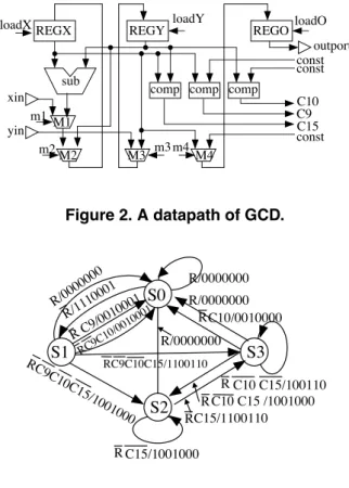
Figure 2. A datapath of GCD.
S0
S1
S2
S3
R/0000000
C10 C15/100110
C15/1100110
C15/1001000 R/0000000
C10/0010000 R/0000000
C10 C15 /1001000 R/0000000
R/1110001 R C9/
0010001 RC9C10/
0010001 RC9C10C15/
1001000
RC9C10C15/1100110
R
R R
R R
Figure 3. A controller of GCD.
module using a combinational ATPG, then find a test plan at an RTL. A test plan is a sequence of control vectors that specifies control paths which justify the obtained tests to the module from primary inputs or control signal lines and observation pathswhich propagate the test responses to pri- mary outputs or status signal lines.
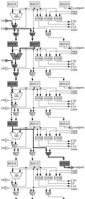
We consider a circuit GCD as an example. Figures 2 and 3 show its datapath and controller, respectively. There are three status signal lines and one primary input of a controller. Figure4 shows control and observation paths where the circuits are expanded to some time frames, where bold lines represent the control and observation paths for a MUX at the second time frame. In the control paths, the left input ports of is controlled directly from a primary input and the right input ports is controlled from whose input ports
are further controlled by paths and
. The observation path is from at the second time frame to the primary output at the 5th time frame where a dotted line means the register holds the value in that time frame. In the first time frame, the left inputs of are selected and registers
load values. These are controlled by a control vector. The test plan is a sequence of such control vectors for these 5 time frames.
REGX REGY REGO
sub comp comp comp
M1
M2 M3 M4
xin yin
const const
const C10 C9 C15
outport
REGX REGY REGO
comp comp comp M1
M2 M3 M4
xin yin
const const
const C10 C9 C15
outport
REGX REGY REGO
sub comp comp comp
M1
M2 M3 M4
xin yin
const const
const C10 C9 C15
outport
REGX REGY REGO
sub comp comp comp
M1
M2 M3 M4
xin yin
const const
const C10 C9 C15
outport
REGX REGY REGO
sub comp comp comp
M1
M2 M3 M4
xin yin
const const
const C10 C9 C15
outport sub
Figure 4. Control and observation paths.
In [7], we defined strong testability of a datapath as testa- bility for hierarchical test for combinational modules. Definition 1 ([7]) A datapath is strongly testable iff there exists a test plan for each module that makes it possible to apply any pattern to and to observe any response of
.
A strongly testable datapath has the following advan- tages. 1) Test pattern generation time is short since a com- binational ATPG can be used, and 2) complete (100%) fault efficiency is achieved for the whole datapath since each
Adder thru
mask 0 0
0
Figure 5. A mask element.
module is a small combinational circuit.
3. Test synthesis using datapath-controller
functions
We consider test plan generation and DFT at the same time. We augment functions of an original controller so as to provide test plans while making a datapath strongly testable. We consider the following test synthesis problem. Input: an RTL circuit (a datapath and a controller) Output: an augmented RTL circuit (a strongly testable dat- apath and a controller capable of providing test plans for each module) and test plans
Objective: minimization of area overhead
We can augment functions of a controller by adding tran- sitions, states, and primary inputs. For a datapath, we add hold function to registers or thru function to modules. Thru function of one input port of a module propagate any value of the input port to its output port without modification. Most of the popular operational modules (e.g. adder) can realize the thru function by using a mask element which generates a constant. Figure5 shows a mask element for an adder.
3.2.1 Idea
We consider how to augment functions of a controller and a datapath so that it can provide test plans like Fig4. Here we consider GCD as an example. Figure3 shows a Mealy FSM of its controller. An output value (i.e. a control vector) at- tached to each transition specifies values of , ,
, , , , in this order. Let
denote a transition from a state to with an input and an output . In the first time frame in Fig4, the left in-
puts of , and are selected and and
load values. This can be represented as a test vec- tor “11x000x” where x means “don’t care”. If the origi- nal controller has a transition that outputs a control vec- tor compatible with this, we may be able to use the tran-
sition. For example, a transition has
a compatible output with “11x000x”. However, we have two more problems. First, we must generate a sequence of control vector provided from a controller. Therefore, if we adopt , the following transition must start from . In our method, we check current and next states as well as output control signals, and if there is no compatible transition we add a new transition to the con- troller. Second, some transition depends on status signals, and it is difficult to control the status signals while generat- ing test plans. To resolve this, we add transitions controlled from outside (additional primary inputs) and independent of status signals. We also augment functions of a datapath. For example, if it is difficult to control all the input ports of some operational module , we add thru function to one input port of and try to control only .
Any augmentation requires some area overhead, and our objective is to find the augmentation with the minimum area overhead. For a datapath, we can easily estimate area over- head required to augment thru function and hold function. For a controller, we introduce a cost function to estimate such area overhead. We propose a branch-and-bound al- gorithm that implicitly searches any possible sequences of transitions and finds the sequence that provides a test plan with the minimum augmentation.
3.2.2 Cost function for controllers
In our method, we do not consider any additional transition requires the same area overhead. For example, consider
the case where we add a transition .
If the original controller already has a similar transition , we can consider this augmentation requires small area overhead. We first define a distance be- tween two transitions and define the augmentation cost for a transition as the minimum distance between and all the existing transitions.
First, we consider a distance of two transitions
and . Each transi-
tion requires a logic that generates the output ( and ) from the input ( and ). We estimate a differ- ence between two logics by the difference between the input and the output of these logics. We treat (“don’t care “) in the different ways for the inputs and the outputs. If an input has , it means that this transition occurs for both and . On the other hand, in an output means this transition gen- erates or . Figure6 shows distance functions of one bit
for inputs (Fig6(a)) and for outputs (Fig6(b)). We can naturally expands these distance functions
for multi-bit. Let and be vectors
of bits. We define and .
For states, we estimate the difference at the worst case.
0 1 x
0 0 1 1
1 1 0 1
x 1 1 0
(a)
0 1 x
0 0 1 0
1 1 0 0
x 0 0 0
(b)
Figure 6. Distance functions: (a) , (b) .
state:s3->s0 vector: 1xxxx111 thru(sub,right) control path: REGY cost:32 state:s1->s0
vector: 1xxxx10 control path: REGX,REGY cost:6
root
state:s3->s0 vector: 1xxxx111 thru(sub,left) control path: REGX cost:22 G state:s0->s1 vector: 1xxxx10 control path: REGX,REGY cost:4
state:s0->s1 vector: 1xxxx101 thru(sub,left) control path: REGX cost:20
state:s0->s1 vector: 1xxxx101 thru(sub,right) control path: REGY cost:20
state: s3->s0 vector: 11xx000 control path: xin,yin cost: 4
state: s3->s0 vector: 11xx100 control path: xin,REGY cost: 5
state: s1->s0 vector: 11xx000 control path: xin,yin cost: 6
nodes for observation paths
Figure 7. Branch-and-bound search
Let be the number of states. In logic level, bit value is assigned to each state. Therefore, we estimate a difference between two difference states to be .
We define the cost function to add a transi- tion to a controller with a state set and a transition set as follows.
if if
For example, consider a cost to add a transition to a controller in Fig3. A distance between an existing transition is as follows. To add , we add a new primary input , and therefore, the
input of becomes . Since values un-
specified in the inputs are “don’t care”,
. Since this is the minimum distance, the cost for is 4.
3.2.3 Branch-and-bound search
We propose a branch-and-bound search algorithm that gen- erates test plans for modules while augmenting functions of both controller and datapath. We will explain how to gen- erate a test plan for one module. The search starts with a tree consisting of one root node. We start the search from the time frame where a test pattern is applied (e.g. the 2nd time frame in Fig4). We consider all possible control and observation paths for this time frame. In the case of in Fig4, we can consider three cases for control paths: one uses both and , the other two use
or and thru function of . In addition, we con- sider every combination of the current and the next states. For each combination of these paths and these states for one time frame corresponds to a transition. Therefore, we can calculate the cost to add the transition. We assign one node for each of these transitions, and make it the child of the root. Then we expand nodes according to a branch-and- bound fashion. That is, in each stage of the search, we select the node such that the total cost from the root to the node is minimum, and generate the child nodes. We first generate nodes corresponding to the preceding transition of control paths as child nodes until all the control paths reach pri- mary inputs, then generate the nodes corresponding to the succeeding transition of observation paths. Once we reach a node where observation path reaches a primary output, the path from the root to the node represents one candidate of a test plan. We then prune any node such that the total cost from the root to the node exceeds the cost of the obtained candidate. Figure7 shows a concept of the search tree, and we omit the detail of the algorithm.
We generate test plans for modules one by one. If the target module has control signals, we generate test plans for each value of the control signal. For example, we generate two test plans for one MUX that apply and for a test pat- tern to the MUX. In such a case, we must apply the search algorithm twice. However, the second search finishes very fast, since our branch-and-bound algorithm searches nodes with low cost first and the test plans obtained at the first search can almost be reused with no cost.
3.2.4 Reduction of the number of test pins
In general, there is a restriction of the number of I/O pins, and therefore, we may have a constraint on the number of additional I/O pins for test (test pins). Though our method requires new test pins to control additional transitions, we can avoid the increase of test pins. Figure8 illustrates the idea to keep the number of test pins. In Fig8(a), we consider to add new transition from to and need an additional test pin since two transitions are already added for test. We avoid the increase by adding a new state and transitions like Fig8(b), where a transition from to outputs the
(a) (b)
s0 s0'
s1 s2 s3
s0
s1 s2 s3
Figure 8. Reduction of the number of test pins.
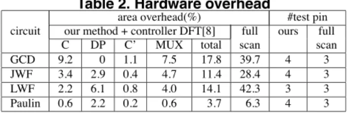
Table 2. Hardware overhead
area overhead(%) #test pin
circuit our method + controller DFT[8] full ours full
C DP C’ MUX total scan scan
GCD 9.2 0 1.1 7.5 17.8 39.7 4 3
JWF 3.4 2.9 0.4 4.7 11.4 28.4 4 3
LWF 2.2 6.1 0.8 4.0 14.1 42.3 3 3
Paulin 0.6 2.2 0.2 0.6 3.7 6.3 4 3
control vectors to hold all the registers. The above tech- nique guarantees that our method is available if at least one additional I/O pin can be used.
4. Experiments
We applied the proposed method to 4 benchmark circuits GCD, 4th Jaumann Wave Filter(JWF), 3rd Lattice Wave Fil- ter(LWF) and Paulin. We compared the results with full scan design reported in [8]. Table1 shows the characteristic of these circuits. The columns #state, #status, #control, #PI,
#PO, bit , #Reg. and #Mod. denote the numbers of states, status signal lines, control signal lines, primary inputs and primary outputs, the bit-width of a datapath, the numbers of registers and modules, respectively. The experiments used a logic synthesis tool AutoLogicII(Mentor Graphics) and an ATPG tool TestGen(Synopsys) on SunBlade1000 (Sun Mi- crosystems). The columns #gate denote the areas of circuits in gates after logic synthesis.
Table2 shows hardware overhead, where C and DP de- note area overhead of augmentation for controllers and dat- apaths, respectively. After the test synthesis for datapaths, we apply the DFT method for controllers proposed in [9]. The column C’ denote area overhead for this controller DFT, and MUX denote area overhead for MUXs to isolate controllers from datapath including MUXs to bring the val- ues of status signals to the primary output of datapaths. The combination of two methods enables test generation using combinational ATPG for the whole RTL circuits.
For these circuits, our method achieves small area over- head, especially for Paulin. We analyzed the result for Paulin more, and found that our method added 7 thru func-
Table 1. Circuit characteristics
controller datapath total
circuit #state #status #control #gate #PI #PO bit #Reg. #Mod. #gate #gate
GCD 4 3 7 169 32 16 16 3 1 1350 1524
JWF 8 0 38 199 80 80 16 14 3 6671 6875
LWF 4 0 8 57 32 32 16 5 3 1924 1986
Paulin 6 0 16 123 64 64 32 7 4 24833 24965
Table 3. Test generation
our method + controller DFT[8] full scan C-ATPG test plan fault eff. test appl. test gen. test appl. circuit (sec) gen. (sec) (%) (cycle) (sec) (cycle)
GCD 0.70 3.71 100.0 774 171.51 6629
JWF 0.54 156.62 100.0 2779 2.88 20519
LWF 0.51 0.96 100.0 394 0.47 4066
Paulin 1.80 252.82 100.0 2703 4.68 16187
tions to the datapath: one for control paths and 6 for obser- vation paths. In our branch-and-bound algorithm, control paths are searched from the target module to primary in- puts, and therefore, we can avoid the augmentation of thru function to some module by controlling the all input ports of the module. On the other hand, we search observation paths from the target module to primary output. In this case, we add thru function to propagate the test response from an in- put port to an output port of a module. This implies that there is still room for improvement in the search algorithm. Table3 shows the result of test generation and test plan generation by our method and full scan design. We gen- erated tests for both datapaths and controllers. Since our method enables us to apply combinational ATPG for each module, time for combinational ATPG is short while achieving 100% fault efficiency. Test application time is much shorter than full scan design. However, for some cir- cuits, our search algorithm consumes time. This is because our algorithm implicitly searches all possible paths.
5. Conclusions
We proposed a test synthesis method that simultaneously considers DFT and test generation for RTL circuits. The proposed method utilizes functions of controller and datap- ath as much as possible. Therefore, we can achieve 100% fault efficiency with small area overhead.
References
[1] B. T. Murray and J. P. Hayes, “Hierarchical test generation using precomputed tests for modules,” IEEE Trans. on Computer Aided Design, Vol. 9, pp. 594–603, June 1990.
[2] Y. Makris and A. Orailo˘glu, “RTL test justification and propagation analysis for modular designs,” Journal of Electronic Testing: Theory and Applications (JETTA), Vol. 13, pp. 105–120, Oct. 1999.
[3] I. Ghosh, A. Raghunathan, and N. K. Jha, “Design for hierarchical testability of RTL circuits obtained by behavioral synthesis,” IEEE Trans. on Computer Aided Design, Vol. 16, pp. 1001–1014, April 1997.
[4] I. Ghosh, A. Raghunathan, and N. K. Jha, “A design for testabil- ity technique for register-transfer level circuits using control/data flow extraction,” IEEE Trans. on Computer Aided Design, Vol. 17, pp. 706–723, Aug. 1998.
[5] I. Ghosh, A. Raghunathan, and N. K. Jha, “Hierarchical test genera- tion and design for testability methods for ASPPs and ASIPs,” IEEE Trans. on Computer Aided Design, Vol. 18, pp. 357–370, March 1999.
[6] S. Ravi, G. Lakshminarayana, and N. K. Jha, “TAO: Regular expres- sion based register-transfer level testability analysis and optimiza- tion,” IEEE Trans. on VLSI Systems, Vol. 9, pp. 824–832, Dec. 2001. [7] H. Wada, T. Masuzawa, K. K. Saluja, and H. Fujiwara, “Design for strong testability of RTL data paths to provide complete fault ef- ficiency,” Proc. of 13th International Conference on VLSI Design, 2000, pp. 300–305.
[8] S. Ohtake, T. Masuzawa, and H. Fujiwara, “A non-scan approach to DFT for controllers achieving 100% fault efficiency,” Journal of Electronic Testing: Theory and Applications (JETTA), Vol. 16, pp. 553–566, Oct. 2000.
[9] S. Ohtake, H. Wada, T. Masuzawa, and H. Fujiwara, “A non-scan DFT method at register-transfer level to achieve complete fault effi- ciency,” Proc. of Asia and South Pacific Design Automation Confer- ence 2000 (ASP-DAC2000), 2000, pp. 599–604.
[10] S. Ohtake, S. Nagai, H. Wada, and H. Fujiwara, “A DFT method for RTL circuits to achieve complete fault efficiency based on fixed- control testability,” Proc. of Asia and South Pacific Design Automa- tion Conference 2001(ASP-DAC2001), 2001, pp. 331–334. [11] S. Nagai, S. Ohtake, and H. Fujiwara, “A method of design for hier-
archical testability for data flow intensive circuits at register-transfer level,” Journal of Information Processing Society of Japan, Vol. 43, pp. 1278–1289, May. 2002.
[12] T. Hosokawa, H. Date, and M. Muraoka, “Test generation method using a compacted test plan table for RTL data path circuites,” Proc. of 20th VLSI test symposium, 2002, pp. 328–335.
[13] H. Date, T. Hosokawa, and M. Muraoka, “A SoC test strategy based on a non-scan DFT method,” Proc. of 11th Asian Test Symposium, 2002, pp. 305–310.