Japan Advanced Institute of Science and Technology
JAIST Repository
https://dspace.jaist.ac.jp/
Title
A 1K-Gate GaAs Gate Array
Author(s)
Ikawa, Yasuo; Toyoda, Nobuyuki; Mochizuki, Masao;
Terada, Toshiyuki; Kanazawa, Katsue; Hirose,
Mayumi; Mizoguchi, Takamaro; Hojo, Akimichi
Citation
IEEE Journal of Solid-State Circuits, 19(5):
721-728
Issue Date
1984-10
Type
Journal Article
Text version
publisher
URL
http://hdl.handle.net/10119/5005
Rights
Copyright (C)1984 IEEE. Reprinted from IEEE
Journal of Solid-State Circuits, 19(5), 1984,
721-728. This material is posted here with
permission of the IEEE. Such permission of the
IEEE does not in any way imply IEEE endorsement
of any of JAIST's products or services. Internal
or personal use of this material is permitted.
However, permission to reprint/republish this
material for advertising or promotional purposes
or for creating new collective works for resale
or redistribution must be obtained from the IEEE
by writing to [email protected]. By
choosing to view this document, you agree to all
provisions of the copyright laws protecting it.
Description
IEEE JOURNAL OF SOLID-STATE CIRCUITS, VOL. SC-19, NO. 5, OCTOBER 1984
A 1K-Gate GaAs
721
Gate Array
YASUO IKAWA, MEMBER, IEEE, NOBUYUKI TOYODA, MASAO MOCHIZUKI,TOSHIYUKI TERADA, KATSUE KANAZAWA, MAYUMI HIROSE, TAKAMARO MIZOGUCHI,
AND AKIMICHI HOJO
Abstract — 1050-gate arrays have been successfully designed and fabri-cated. Chip size is 3.75X 3.75 mm. A basic cell can be programmed as an E/D-type DCFL three-input NOR gate. Speed performance measured at 0.2 mW/gate power dissipation was as follows. Unloaded (fanout = 1) propagation delay time was 100 ps/gate. Load dependence of the delay time was 65 ps/1 mm interconnection line, 27 ps/fanout, and 3.33 ps/crossover load. This leads to 350 ps/gate delAy under the assumed loading condition of interconnection line length= 3 mm and three fanouts.
The gate array was applied to a 6x 6 bit parallel multiplier circuit. The 10.6 ns multiplication time was measured at 380 mW power constrmption. The operation speed of the personalized circuit can be well described by the basic performance provided by ring oscillator measurement.
I. INTRODUCTION
T
EN years have passed since the first GaAs digital IC was reported in this journal [1]. Great progress has been made in GaAs material and process technology, espe-cially for the past several years, which has brought state-of-the-art GaAs IC’S into LSI level integration [2]-[5].From the system viewpoint, more and more logics are desired to be integrated in a single chip to make the best of GaAs high-speed capability. The reason is that the multi-SSI/MS~ chip system has to include rnillimeter/centime-ter-range interconnections between chips, where even an electromagnetic wave requires 10–100 ps to travel, while the propagation delay inside the GaAs IC chip is almost in the same time range. Among the several circuits available to GaAs, which include BFL, SDFL, DCFL, and SCFL, DCFL (direct-coupled FET logic) is the simplest and shows the least power consumption. It seems that only DCFL can realize more than several thousand gate logics in a chip, taking into account the power limit in a single chip.
The gate array approach is also effective for GaAs as well as for Si IC’S in enabling logic designers to obtain desired logic functions relatively easily. To date, GaAs gate arrays with hundreds of gates in a chip have been reported [6]-[9].
This paper reports on the successful fabrication of a lK-gate GaAs gate array using DCFL circuitry, em-phasizing that the GaAs DCFL has the potential of obtain-ing high speed and higher integration than any other
Manuscript recewed March 27, 1984; revised May 29, 1984. This work was supported in part by the Ministry of International Trade and In-dustry (MITI) of Japan in the framework of the national research and development project ‘<Scientific Computing System.”
The authors are with Toshiba Research and Development Center, Kawasaki 210, Japan.
circuitry. Application to a 6 X 6 bit parallel multiplier and its complete operation will also be described.
II. DESIGN
A. FET Size Determinatiott
The gate array performance largely depends on the FET size for each gate. Prior to the final design, three kinds of gate array basic cells were fabricated and evaluated. Basic cells were implemented by E/D-type DCFL to m~ake three-input NOR programmable. The three kinds include EFET/DFET gate widths of 10/5 (type A), 20/10 (type B), and 40/20 (type C) in microns, respectively. Loaded propagation delay time versus power dissipation character-istics were measured, taking basic cell FET size a.s a parameter. Empirical loaded propagation delay time tpd is given by
tpd= tpdl+( F–l).Atpd~+ L“AtpdL + c’A~p~c where
tpdl= unloaded (fanout =1) propagatio~ delay time AtPdF = increase in delay time/ fanout
AtpdL = increase in delay time/unit ifitercortnection length
Atpdc = increase in delay time/one crossover load F = number of fanouts
L = interconnection line length C = number, of crossovers as a load.
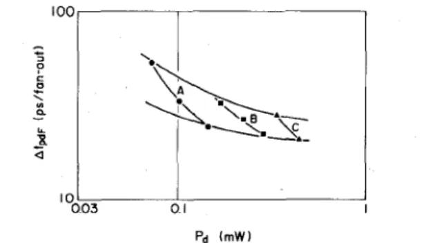
AtPdF, AtPd~, and Atpdcas functions of power dissipation and basic cell FET size are shown in Figs. 1, 2, and 3, respectively. These data have been obtained by measuring the waveforms of 15-stage ring oscillators with various kinds of loads listed in Table I. Fig. 4 shows the gate array chip, where seven different ring oscillators are constructed using 20/10 pm EFET/DFET gate width (type B). Gate arrays for the other two types of basic cells (types A and C) were also fabricated on the same wafer. Thus, pra,cess conditions are completely the same through types A,, B, and C, The design rules for these three types of ring oscillators are also identical, except for gate width. There-fore, the measured characteristics can be directly compared with each other. Comparison results indicate gate width tradeoffs for basic cell FET’s.
722 IEEE JOURNAL OF SOLID-STATE CIRCUITS, VOL. se-l 9, NO, 5, OCTOBER 1984
10
0.03 0. I I
f’d (mW)
Fig. 1. Propagation delay time increase per fanout as functions of power dissipation and basic cell FET size. V~~ = 1 V.
‘;,
o. IPd (mW)
Fig. 2. Propagation delay time increase per 1 mm interconnection line load as functions of power dissipation and basic cell FET size. V~~ = 1 V.
40rT__l
“,,o~
oIP~ (mW)
Fig. 3. Propagation delay time increase per one crossover load as func-tions of power dissipation and basic cell FET size. V~~ = 1 V,
Figs. 2 and 3 show that the switching energy for an additional load is constant, regardless of the basic cell FET size. This is supported by the following simple analysis.
Given load capacitance CL, electric charge Q is ex-pressed as
Q = CL.AVX ictpd (1)
where AV is the E/D DCFL logic swing, ic is the charging
TABLE I
RING OSCILLATORS WITH VARIOIJS KINDS OF LOADS
15-stage
ring oscil Iators Loading condition F.O. = I F.O. = 3 F.0, =5 L =Imm L =2mm L =3mm Numberof cross-over =64
Fig. 4. Gate array performance evaluation chip. 15-stage ring oscillators using 20/10 pm wide EFET/DFET DCFL basic cells with various kinds of loads are constructed. The chip configuration is the same as the final version of the 1K-gate gate array.
current, and tpd is the propagation delay time. i ~ is de-termined by the saturation current for load DFET. Power dissipation Pd is proportional to icVDD, where V~~ is the supply voltage. Thus,
Pd ~ icV~~. (2)
Equations (1) and (2) yield
W= Pdtpd a C~.AV.V~~. (3) It can be concluded that Pdtpdis constant with a fixed
load capacitance, even if FET size is changed.
For fanout dependence, simple analysis by (1) gives
lKAWA et al.: 1K-GATE GaAs GATE ARRAY 723
Pd ( mW/gate)
Fig. 5, Propagat~on delay time versus power dissipation for compact ring oscillators as a function of basic cell FET size
Pad
1/0 Buffer
vD~
Fig. 6 Chip design representation for the final version of lK-gate gate array.
Therefore, AtP~F ideally does not depend on FET size. The same conclusion can be applied to intrinsic propagation delay time tPdO, measured on the compact ring oscillators, where interconnection line length between inverters is laid out to be minimized (Fig. 5). Both AtP~F and tpdohave a little bit larger value for type A than for the other two types. This implies that parasitic capacitance exists, which cannot be counted as either interconnection line or cross-over load. This parasitic capacitance might be associated with the FET electrode layout. However, details are not known.
These measured data served as support materials for making the decision in regard to FET size. The decision was also made, taking into account the required gate array specifications on speed, power, and chip size.
Type B was adopted as the final design for lK-gate gate array, because of its AtpdFadvantage over type A and smaller power consumption than type C, with almost the same AtPdF value. The 0.2 mW/gate power dissipation for type B is also favorable, when targeting future several-thousand-gate gate arrays, which makes the lK-gate gate array a good experimental step towards higher integration. B. Chip Layout
Fig. 6 shows the schematic representation of the final
version of the lK-gate GaAs gate array. It is identical with the chip shown in Fig. 4 and also with the application chip described later.
Chip size is 3.75x 3.75 mm. Fig. 7 shows the layout and the equivalent circuit representation for the basic cell,
VDD GND GND (a) ~Do , --- --- . . . ..--- . . . .. . . . .
“’l+f~-”-”
---
______
:---}
____
(b)Fig. 7. Basic cell used in the chip shown in Fig, 6, (a) Layout (b) Equivalent circmt representation. EFET/DFET gate width is 20/10 pm.
which measures 34x 75 pm and can be programmed as a DCFL three-input NOR gate. The nominal gate width/ length values are 10/1 (pm) for DFET load and 20/1 for EFET drivers. Source and drain contacts are formed onto the heavily doped n-t ype region and nominal n ‘-n+ spac-ing is 2 v m. There are 14 columns and each column has ’75 basic cells, totalling 1050 gates in a chip. Between the columns, there are 13 interconnection tracks whose wicIth is 108 pm. The design rules of 2 pm line width, 3 pm line spacing, and 2x 2 pm contact hole allow 13 first-level interconnection lines to run in each track parallel to the column direction. The second-level interconnection lines (3 pm wide and 4 pm spacing) can run across the column with the restriction that they should not run above the F13T gate region. Actually, three second-level line can run across the basic cell, which is not used as a gate, or one second-level line can run across the basic cell in use.
In order to avoid the low noise margin problems associ-ated with DCFL circuitry, various measures were em-ployed for the power supply line layout, especially for the ground lines. Among them was the layout wherein ground lines were realized by second-level metallization to mini-mize sheet resistance. In addition, a ground line which is connected to each basic cell runs vertically to the column direction, which reduces the number of basic cells con-nected to each ground line, resulting in low current and low voltage drop in each ground line. In the design phase, power supply lines are laid out so that the potential diff-erence between ground level for any basic cell and ground pad should be less than 50 mV and the voltage drop at any point in the V~~ lines should be less than 200 rnV.
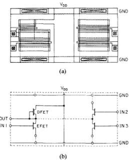
Surrounding the array region are the V~~ and ground (GND) main lines, and 56 1/0 buffers and pads. Two ~9~ and two GND pads are also provided.
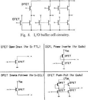
The circuit used for an 1/0 buffer is shown in Fig. 8. It consists of 2 DFET’s and 8 EFET’s. All FETs have 80 pm
724 IEEE JOURNAL OF SOLID-STATE CIRCUITS, VOL. SC-19, NO. 5, OCTOBER 1984
Fig. 8. 1/0 buffer cell circuitry
EFET Open Dram (fOr SI-TTL) DCFL Power I nverter (for GoAs) “ Vm
-T”
DFET
EFET * EFET
DFET Sowce Follower (for SI-ECL) EFET Push-Pull (for GaAs) , v..
Fig. 9. Examples of output buffer circuit programming
gate width. They can be programmed as either an input or output buffer.
It is well known that there is an orientation effect on GaAs MESFET I-V characteristics [10]. In order not to be affected by this effect, all the FET’s are placed parallel to each other in terms of gate width direction, including 1/0 buffers and basic cells. Therefore, the 1/0 buffer cell is designed to be square-like in shape to aid in achieving a space-efficient layout. As a result, the 1/0 buffer cell occupies an about 110X 120 pm area adjacent to a pad.
Input buffers are DCFL power inverters. As shown in Fig. 9, available output buffers include EFET open drain circuits for Si–TTL interfaces. DFET source followers for Si-ECL interfaces, DCFL power inverters, and EFET push-pull circuits for interfacing with GaAs circuits of the same type. A specific buffer can be selected by the inter-connection layout masks for each interfacing purpose.
111. FABRICATION PROCESS
Table II summarizes the fabrication process used for lK-gate gate array. The key feature is the Pt-buried gate technique, which uses the Pt reaction with GaAs at around 400”C to control FET threshold voltage [11]. Average threshold voltage was 0.1 V for EFET and – 0.7 V for DFET. Standard deviation in the threshold voltage was 53 mV for EFET’s and 110 mV for DFET’s across a wafer.
Thickness and sheet resistivity values were 6000 A and 0.1 0/0 for first-level metallization and 1.2 pm and 0.02 fl/cI for second-level metallization.
Lithography used through all processes was optical with contact/proximity exposure.
IV. GATE ARRAY PERFORMANCE
Examples of EFET and DFET 1-V characteristics used in basic cells are shown in Fig. 10. As described in Section II, propagation delay time dependence on the
interconnec-TABLE II
FABRICATION PROCESSFOR lK-GATE GAAS GATE ARRAY
● Substrate Cr-doped 2“.#1 LEC wafer
● Active layer formotton 28 SI+ selectwe implontofion dwectly mto the substrate {
n+ -Source 13 Droin 200 keV 30x IOL3 cm-z DFET [50 keV 2.s3x1012 cm-z EFET 100 keV 3,2x 1012 cm-z
● Annealing Capless 850”C 15 mm AsH3 + Ar
● Ohmic contact AuGe/Au 420”C 2mm OIIOY
● Gate metol Pt(50 nm) 400”C smtermg
● I st metal T1/Pt /Au 9 Spocmg d!electrlc CVD SIOZ (600nm)
● Contact hole Au VIQ metal
● 2nd metal TI /Pt /Au
ID- VD curve & -Vcj plot
ID & (mA) [A) Im :% 0 IX& 3WJ /d,” Ocox Ocma
Ooxm 2mo O&Xc moo
Vo Omldlv (v) VG 700)/d,v (mV) VG=O-. O7(V), Ol(V) step VD= l(V), fixed
Wg/Lg=20/lpm (a) lD-VD curve ID [PA) 0 V, OXY.XI/d,v WI VG=-lO-O(V). O l(V) step & -v~ plot fio {./T) :L& 31Xm fd(” o~ecc Oeccm Vc. 0 Im/dl” w) VO= I (V). fixed WQ/Lg=lO/lpm (b)
Fig, 10. Examples of EFET(a) and DFET(b) I-V characteristics used m a basic cell.
tion line length and the number of fanouts and crossovers was evaluated by measuring ring oscillators under various loads at F“DD = 1 V. The obtained results are as follows.
The unloaded propagation delay time was 100 ps/gate and the delay time increased at a rate of 65 ps/mm, 27 ps/fanout and 3.33 ps/crossover at power dissipation of 0.2 mW/gate, where nominal crossover area was 2 x 3 pm. This leads to tpd= 350 ps/gate under an assumed loading condition of interconnection line length = 3 mm and three fanouts.
SPICE-H simulation was performed to understand ring oscillator operation. The SPICE-H JFET model was ap-plied. Using EFET and DFET Z- V characteristics shown in Fig. 10 and assuming 0.9 fF/pm2 nonbiased gate junction capacitance, the simulated unloaded delay time coincided very well with the measured value. The simulation also
IKAWA et al.: lK-GATE GaAs GATE ARRAY TABLE III
725
PERFORMANCE OF lK-GATE GAAS GATE ARRAY
Chip size Basic cell FET swe(mask) FET source -drom
spocmg Desagn rule for
mterconnectlon Ist level 2nd level contact hole FET performance measured 9rn V,h” LQ(gote Ienqth) Propqohon delay hme
unloaded (fen-wt=ll power level dependence on tom
Propagation deloy time under 100ding conditmn of L=3mm, Fon-wt=3
375mm~375mm 3-INPUT NOR IDCFLI 10/1 (pm] DFET load 20/l (pm) EFET driver 2pm
In+ -source, dram)
2-Pm wide. 3-Pm spacing 3-Pm wide. 4-pm spacing 2+m x 2pm 110 mS/mm 01 V(EFETI. -O7V(OFET) 10pm 100 ps/gOte 02 mW/gote 27 ps/fon- out 65 ps/mm 333 pslcross-over 350 ps/gOte (O 2 mW/gOte )
showed that additional fixed 1 fF capacitive load increases delay time by 1.09 ps. This value was combined with the measured tpddependence on interconnection line length ( =65 Ps/mm), and it was found that first-level intercon. nectlon hne capacitance was 60 fF/mm, which agrees very well with the numerically calculated value reported elsewhere [12].
The gate array performance is summarized in Table III.
V. APPLICATION
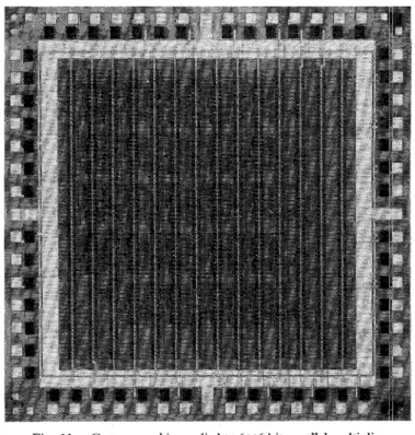
The gate array has been applied to a 6x 6 bit parallel multiplier circuit. Fig. 11 shows the applied gate array chip. 378 internal gates and 24 1/0 buffer cells are used to implement the circuit employing a carry-save algorithm, which is illustrated in Fig. 12. The critical path is shown by the thick arrow in the figure. A full adder (FA) and half adder (HA) are constructed using NOR gates and inverters, as shown in Fig. 13.
Approximately 70 percent of the array area is occupied for interconnection purposes. Layout is not compact and is not optimized. However, this layout appeared to be good enough to demonstrate the feasibility of using the GaAs gate array at lK-gate level integration. Output buffers selected were 160 pm wide EFET push-pull circuits.
A functional test was performed at V~~ = 1.5 V. An example of low frequency test results with high load
im-pedance at the output buffer is shown in Fig. 14. The input data pattern was 10000S X 111111. A sequential 0/1 pulse was applied to the least significant input bit AO. This test is the so-called ripple test. Complete operation was con-firmed, as shown in the figure. Logic swings at all outputs are large enough to drive DCFL inputs of other GaAs IC’S.
Fig. 11. Gate array chip applied to 6 x 6 bit parallel multiplier.
Multiplication time measurement was also performed for the chip which passed the low frequency test. The test pattern for multiplication time measurement was S000011 X 111111. S went from the O to the 1 state and was applied to the most significant input bit A5. Fig. 15 shows the waveforms of product bits P1O and Pl 1 measured by wafer probing. The probe system was a 50 !2 system, calibrated for high-speed testing. The rise time of the applied input was about 2 ns, which was determined by the pulse generator performance used and the bandwidth of the wafer probing system. Multiplication time is the time between the input rise and the P1O output fall. It is not clear at which moment the input rise signal transient makes the input buffer invert the signal. It is also not clear which moment of the down slope for the P1O output waveform reveals the multiplication completion point. In spite of these uncertain factors, it can be said that the multiplicat-ion time is less than 10.6 ns, where total power consump-tion is 380 mW, including 1/0 buffer circuit operation.
On the other hand, multiplication time was calculated using the gate array performance data listed in Table III. The loading conditions at a specific logic gate along the critical path were evaluated by looking at the actual layout to calculate propagation delay time at the gate. ?vfultip’lica-tion time was calculated as the sum of the propagation delay times at each gate along the critical path. The calcu-lated multiplication time was 8.5 ns. This agrees fairly well with 9 ns, which is the measured value obtained by talhg the time between the middle of the input rise and the moment when the output just begins to fall as the mult impl-ication time.
Therefore, the speed performance of the personalized gate array can be reasonably explained and estimated, using the basic performance obtained through ring oscilla-tor results.
726 IEEE JOURNAL OF SOLID-STATE CIRCUITS, VOL SC-19, NO 5, OCTOBER 1984
E
i“,FA15, b$.hb, A3E5 w 44 & PI, P,. P9 Fig. 12. Ful I Adder Half A— B~111
P8 P, P6 4, U,WC 8 tiA2 42 FA I wi!!
HAT.
FA16 P5 P4 A B RRY c’ M Adder T i P2Block diagram for 6x 6 blt parallel multlpher. Carry-save al-gorithm is used. Thick arrow shows the critical path.
~“”y
Fig 13. Block dmgram for full adder (FA) and half adder (HA) used in 6 X 6 blt parallel multiplier,
The logic swing obtained in high-speed testing is 230 mV, as shown in Fig. 15. Thus, the current driven by a 160 pm wide EFET push-pull output buffer is estimated to be 230 (mV)/50 (Q)= 4.6 mA. This indicates that the output buffer speed is 2.2 ns when driving the assumed 10 pF external capacitive load to obtain 1 V logic swing. It might also be the case with other types of output buffers like the 160 pm wide EFET open drain and the 160 pm wide DFET source follower, which is implied by the 1-V curves for 20 pm wide EFET and 10 pm wide DFET, as shown in Fig. 10. However, they have not been directly measured yet.
VI. CONCLUSION
A 1050-gate GaAs gate array has been successfully fabricated using DCFL circuitry. It features 350 ps/gate propagation delay at 0.2 mW/gate power dissipation
un-4080 +-% / 0 AO Po PI P2 P3 P4 P5 AO P6 P7 P8 P9 Plo Pll
Fig 14 Outputs of 6 X 6 bit parallel multiplier at low frequency test, Input code is 10000S X 111111 = SSSSSSSSSSSS, where S M sequen-tial 0/1 pulse applied to ,40. VD~ = 15 V, P = 380 mW
der the loading condition of 3 mm interconnection line length and three fanouts. A 6X 6 bit parallel multiplier was constructed on the gate array. The multiplication time was measured to be 10.6 ns at 380 mW overall power consump-tion.
Gate array performance is compared with other logic families on the basis of speed, power and integration. as
IKAWA et al.: lK-GATE GaAs GATE ARRAY 727
A5
Plo
A5
Pll
Fig. 15. Output wav~orms for product bits P1O and Pll, when ,S00001 X 111111= S00000S11111 multiplication was performed. ,S is the pulse applied to ~ 5, which changes from O to 1 state. At first, output F’1O rises, responding to fast arrival of ,45 B5( =1) calculation at FA 24, It then returns to zero as a result of carry signal from FA 23to M 24. This corresponds to the critical path of the multiplier. V~~ = 1,5 V, P = 380 mW,
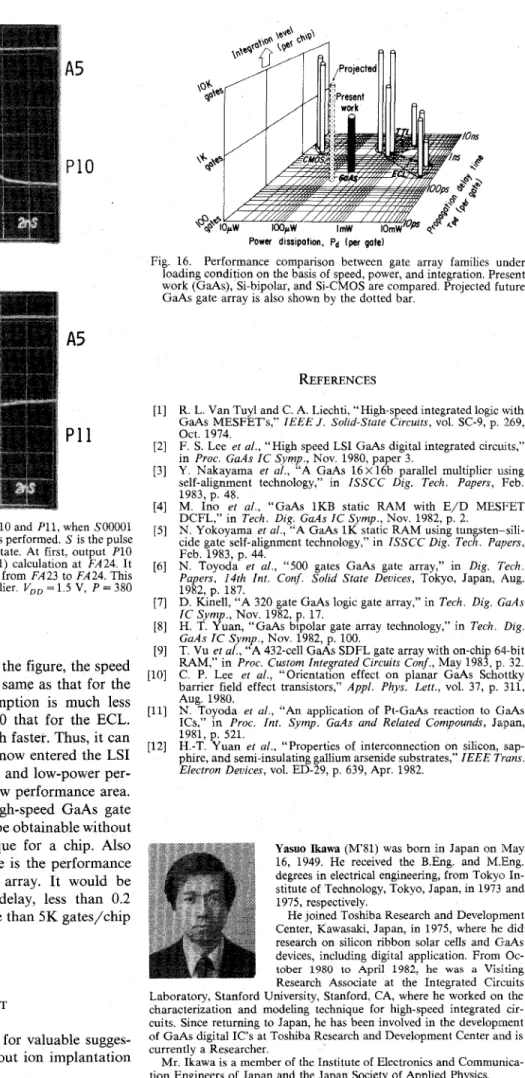
shown in Fig. 16. As is clearly seen in the figure, the speed for the GaAs gate array is almost the same as that for the Si-ECL. However, the power consumption is much less than for the ECL, that is about 1/10 that for the ECL. Comparing with CMOS, GaAs is much faster. Thus, it can be said that the GaAs gate array has now entered the LSI integration level with both high-speed and low-power per-formance and seems to fit into the new performance area. This performance indicates that a high-speed GaAs gate array with several thousand gates will be obtainable without introducing a special cooling technique for a chip. Also shown by the dotted bar in the figure is the performance for the projected future GaAs gate array. It would be featured by less than 200 ps/gate delay, less than 0.2 mW/gate power dissipation, and more than 5K gates/chip integration.
ACKNOWLEDGMENT
The authors wish to thank Dr. Nii for valuable sugges-tions and Mr. Ishimura for carrying out ion implantation and helpful discussions.
Power d~ssipotion, Pd (per gate)
Fig. 16. Performance comparison between gate array families uuder loading condition on the basis of speed, power, and integration, Present work (GaAs), Si-bipolar, and Si-CMOS are compared. Projected future GaAs gate array is also shown by the dotted bar.
FU3FE~NCES [1] [2] [3] [4] [5] [6] [7] [8] [9] [10] [11] [12]
R. L. Van Tuyl and C. A. Liechti, “High-speed integrated logic with GaAs MESFET’S,” IEEE J. So[id-Stale Circuits, vol. SC-9, p. :269,
Oct.1974.
F. S. Lee et a[., “High speed LSI GaAs digital integrated circuits,” in Proc. GUAS IC Synrp., Nov. 1980,paper 3.
Y. N~ayama et a/., “A GaAs 16X 16b parallel multiplier using self-ahgnment technology,” in ISSCC Dig. Tech, Papers, Feb. 1983, p. 48.
M. Ino et al., “ GaAs lKB static RAM with E/D MESFET DCFL,” in Tech. Dig. GaAs IC Symp., Nov. 1982, p. 2.
N, Yokoyama et al., “A GaAs lK static RAM using tungsten-- sili-cide gate self-alignment technology,” in ISSCC Dig. Tech. F’qoers, Feb. 1983, p. 44,
N. Toyoda et al., “500 gates GaAs gate array,” in Dig. Tech. Papers, 14th Int. Conf. Solid State Devices, Tokyo, Japan, Aug. 1982, p. 187.
D. Kinell, “A 320 gate GaAs logic gate array,” in Tech. Dig. GaAs IC Swnr).. NOV. 1982. t). 17.
H. T“. ~uan, “ GaAs &polar gate array technology,” in Tech. Dig. GaAs IC Symp., Nov. 1982, p. 100.
T. Vu et al., “A 432-cell GaAs SDFL gate array with on-chip 64-bit RAM,” in Proc. Custom Integrated Circuits Conf., May 1983, p. 32. C. P. Lee et al., “Orientation effect on planar GaAs Schottky barrier field effect transistors,” Appi. Phys. I&W., vol. 37, p, 311, Aug. 1980.
N. Toyoda et al., “An application of Pt-GaAs reaction to GaAs ICS,” in Proc. Int. Symp. GaAs and Rekxed Compounds, Jarpan, 1981, p. 521.
H.-T. Yuan ei al., “Properties of interconnection on silicon, sap-~hire. and semi-insulating ~allium arsenide substrates,” IEEE Trans. Electron Devices, vol. E~-~9, p. 639, Apr. 1982
Yasuo Ikawa (M81) was born in Japan on May 16, 1949. He received the B.Eng. and M.lEng. degrees in electrical engineering, from Tokyo In-stitute of Technology, Tokyo, Japan, in 1973 and 1975, respectively.
He joined Toshiba Research and Development Center, Kawasaki, Japan, in 1975, where he did research on silicon ribbon solar cells and GaAs devices, including digital application. From Oc-tober 1980 to April 1982, he was a Visiting Research Associate at the Integrated Circuits Laboratory, Stanford University, Stanford, CA, where he worked on the characterization and modeling technique for high-speed integrated cir-cuits, Since returning to Japan, he has been involved in the development of GaAs digital IC’S at Toshiba Research and Development Center and is currently a Researcher.
Mr. Ikawa is a member of the Institute of Electronics and Communica-tion En@eers of Japan and the Japan Society of Applied Physics.
728
Nobuyuki Toyo&a, for a photograph and biography, see this issue, p. 715
Masao Mochizuki, for a photograph and biography, see this issue, p. 715
Toshiyuki Terada, for a photograph and biography, see this issue, p. 715
Katsue Kanazawa, for a photograph and biography, see this issue, p, 715
IEEE JOURNAL OF SOLID-STATE CIRCUITS, VOL. se-l 9, NO.5,OCTOBER 1984 Mayumi Hirose received the B.S. and M.S. de-grees in chemistry from Ochanomizu University, Tokyo, Japan, in 1980 and 1982, respectively.
In 1982, she joined Toshiba Research and De-velopment Center, Kawasaki, Japan. She has been engaged in the reserach and development of GaAs digital IC’S.
Miss Hirose is a member of the Japan Society of Applied Physics and the Institute of Electron-ics and Communication Engineers of Japan.
Takamaro Mizoguchi was born in Yokohama, Japan, on February 13, 1945. He received B.S. and M, S, degrees in chemistry from the Univer-sity of Tokyo, Tokyo, Japan, in 1968 and 1970, respectively.
He joined the Research and Development Center, Toshiba Corporation, Kawasaki, Japan, in 1970. He has been engaged in the development of semiconductor integrated circuit technology, and is currently concerned with GaAs digital integrated circuits.
Mr. Mizoguchi is a mem{er of the Institute of Electronics and Com-munication Engineers of Japan.
Akimichi Hojo, for a photograph and biography, see this issue, p. 715.
A Gallium Arsenide
Configurable
Cell
Array Using Buffered
FET Logic
ROBERT N. DEMING, RICARDO ZUCCA, SENIOR MEMBER, IEEE, RICHARD l?. VAHRENKAMP, L. DANIEL HOU, BARBARA A. NAUSED, AND BARRY K. ~ILBERT, MEMBER, IEEE
Abstract — A GaAs configurable cell array has been fabricated using 1 pm gate MESFET’S on 3 in GaAs substrates trsing a planar f abdication technique. Depletion-mode MESFET’S configured in BFL strictures were used to ismp!ement the logic cells. The cells are programmable for several logic functions mrd two different drive capabilities. Placement and routing software was deveioped. Cell configuration and army organization were adjusted to optimize the efficiency of the placing and touting software. Measured results on several cell configurations with various device sizes yielded speed-power products ranging from 162 to 460 f.1. A 306 cell array (equivalent to approximately 430 NOR gates) occupying a chip area of 2.0 X 2.8 mm was fabricated. A 5X 5 bit paraBel ntrrltiplier implemented
Manuscript received March 12, 1984; revised May 16, 1984. This work was supported in part by the Defense Advanced Research Projects Agency under Contracts F49620-83-C-O042 and MDA903-82-C-0175.
R. N. Deming was with the Microelectronics Research and Develop-ment Center, Rockwell International, Thousand Oaks? CA 91360. He is now with Vitcsse Electronics Corporation, Westlake Vdlage, CA 91362.
R. Zucca, R. P. Vahrenkamp, and L. D. Hou are with the Microelec-tronics Research and Development Center, Rockwell International, Thousand Oaks, CA 91360.
~. A. Naused and B. K. Gilbert are with the Special Purpose Processor Development Group, Mayo Foundation, Rochester, MN 55905.
with this array showed a multiplication time of 6.5 ns, and a power dissipation ranging from 337 to 722 mW corresponding to a cell power of 1.30-2.79 mW/ceK
I. INTRODUCTION