Kota TERAI†a), Emi KAWASHIMA†, Naoki KURIHARA†, Hideaki NAGASHIMA†, Hirofumi KONDO†, Masatoshi SAITO†, and Hiroaki NAKAMURA†, Nonmembers
SUMMARY We have succeeded in developing high-performance p-type of organic semiconductors with phenylethynyl groups, which have high filed-effect mobilities (> 3 cm2V−1s−1) by improving molecular pla-narity. A single crystal of the organic semiconductors has a herringbone structure. It plays an important role for carrier transport. In addition, we found that they had lower contact resistances to Au electrodes as well. Then, we used the materials for the carrier injection layer deposited onto another organic semiconductor we developed recently, which achieved a high field-effect mobility, and a low threshold voltage (Vth).
key words: organic semiconductor, OTFT, herringbone structure, contact
resistance
1. Introduction
Organic thin film transistors (OTFTs) have several advan-tages for electronic devices, such as low cost, flexibility and light weight [1], [2]. Furthermore, it has attracted much attention in large-area applications including flexible cir-cuits, such as sensors [3], light emitting diodes [4], solar cells [5], [6] and flexible displays [7] since it was found that field-effect mobilities of several compounds exceeded that of amorphous silicon.
We have been developing organic semiconductors for OTFTs and we reported oligo-p-phenylenevinylenes showed good performances. 1,4-Bis(4-methylstyryl) benzene (4MSB) has a high field-effect mobility of 0.13 cm2V−1s−1[8], [9]. However, an OTFT needs a higher
field-effect mobility and a lower threshold voltage to be commercialized for flexible displays. In order to achieve a higher field-effect mobility, we focused on a molecular structure to improve the molecular design. As the result, we have succeeded in developing 2,6-Bis(2-phenylethynyl) an-thracene (DPEA) as a new p-type of organic semiconductor which designed to improve planarity of a molecule.
In this report, we studied material properties, such as crystal structure of single crystals, growth mechanism of thin films and contact resistances (RCs) to achieve the
high field-effect mobility of over 3 cm2V−1S−1. In addition,
DPEA was found to have good carrier injection characteris-tics by RCmeasurement. We fabricated OTFT devices with
the DPEA as a carrier injection layer on the other organic semiconductor.
Manuscript received March 24, 2011. Manuscript revised June 7, 2011.
†The authors are with Idemitsu Kosan Co., Ltd.,
Sodegaura-shi, 299-0293 Japan.
a) E-mail: [email protected] DOI: 10.1587/transele.E94.C.1713
2. Experiments
4MSB was purchased from Tokyo Chemical Industry Co., and DPEA was synthesized using Sonogashira coupling re-action. The chemical structures of 4MSB and DPEA are shown in Fig. 1. All of the semiconductors were purified by train sublimation under high vacuum of 7.0 × 10⁻⁶Pa. The purity was evaluated to exceed 99% measured by high performance liquid chromatography (HPLC).
Single crystals of the organic semiconductors which were suitable for X-ray analysis were obtained by the fol-lowing sublimation method: the materials were placed in-side an edge of glass tubes (630 mm in length and 28 mm in diameter). The tubes were evacuated and the air was re-placed with nitrogen. The tubes were sealed under pres-sure of around 0.1 atm and then the source materials were heated to 260◦C for 4MSB and 240◦C for DPEA respec-tively and 150◦C at the other edge. X-ray diffraction (XRD) data on single crystals were measured by a Rigaku AFC10 diffractometer (Mo-Kα radiation, λ = 0.71070 Å, graphite monochromated). The single-crystal structures were solved by direct methods. Non-hydrogen atoms were refined anisotropically, and all hydrogen atoms were inserted at cal-culated positions. By using the result of the single crystal analysis, all calculations were performed using the crystal-lographic software package Crystal Structure Version 2.00. The bandwidths were calculated with framework of the tight-binding theory as proposed by Br´edas and co-workers [10], using the semiempirical intermediate neglect of dif-ferential overlap (INDO) method employed in Gaussian 03 [11].
We fabricated top-contact OTFTs as shown in Fig. 2, using two types of substrates. One is a glass substrate with a poly (chloro-p-xylylene) (Parylene-C) insulator [12], the other one is a Si substrate with a thermal oxidized SiO2gate
insulator (300 nm). In the case of Si substrate, a SiO2
sur-face was treated by hexamethyldisilazane (HMDS) [13] or polystyrene (PS) [14] with a thickness of 20 nm to obtain
Fig. 1 Chemical structure of 4MSB and DPEA.
Fig. 2 Illustration of the top-contact device structure on the glass substrates.
a lower surface energy. The organic semiconductors were evaporated under a pressure of below 2× 10⁻⁴Pa at a depo-sition rate of 0.05 nm/s to form a layer with a thickness of 40–50 nm on the substrate at room temperature. Au source-drain electrodes were evaporated through a shadow mask with a thickness of 50 nm on the semiconductor. The chan-nel length L and width W were 50μm and 1 mm, respec-tively. In the case of a glass substrate, we used an indium-tin-oxide (ITO) layer sputtered onto a glass substrate with a thickness of 130 nm as a gate electrode. The ITO film was patterned by a conventional photolithography technique to form 6-mm-wide, 25-mm-length stripes. Subsequently, the Parylene-C was deposited by thermal chemical vapor depo-sition at a thickness ranging from 500 to 800 nm to serve as a gate insulator. The organic semiconductors and the elec-trodes fabricated under the same conditions as that in the case of the Si substrate. The fabricated devices annealed at 100◦C in 3 hours in a glove box with under N2atmosphere.
All devices were temporarily exposed to air prior to conducting measurement and the measurement was con-ducted under vacuum conditions using Keithley 4200SCS Semiconductor Parameter Analyzer.
The electric parameters were estimated in OTFTs us-ing a standard analytic theory of metal-oxide-semiconductor field-effect transistor. Above threshold voltage, the drain current tends to saturate due to the pinch off of accumula-tion layer, and is modeled by
ID=
WC
2L μ(VG− VT)
2, (1)
where, W and L are the channel width and length, C is the capacitance per unit area of the insulator, VGand VT are the
gate and threshold voltage andμ is the field-effect mobility in channel regime. The field-effect mobility can be calcu-lated from the slope of the plot of|ID|1/2versus VG.
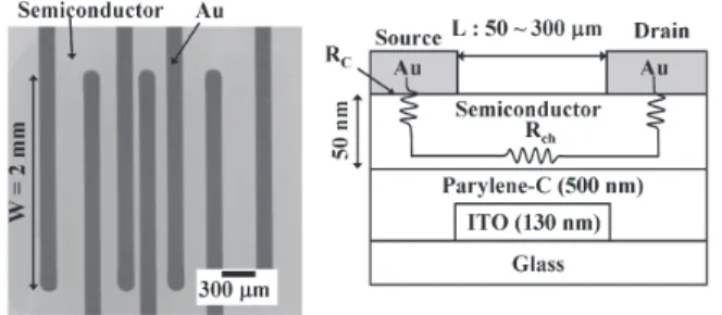
The contact resistances between the electrode/semi-conductor interfaces were evaluated by the transmission line model (TLM) [15]–[17]. We fabricated six devices having an identical channel width (2 mm) and varied channel length (L= 50–300 μm). DPEA and pentacene were deposited as semiconductor onto Prylene-C insulator. Figure 3 shows an optical micrograph of a device for TLM measurement with different channel length and a schematic illustration of tran-sistor with cross section describing RC.
In the linear regime, the total resistance (Rtot) of an
OTFT can be explained as the sum of channel resistance (Rch) and RCas below
Rtot= Rc+ Rch, (2)
Fig. 3 Optical micrograph of TLM device (left) and schematic transistor cross section describing RC(right).
Rch=
L
μWC(VG− VT).
(3) This equation indicates that we can obtain RC by
extrapola-tion of L to zero along the line of the channel length depen-dence of Rtot.
Crystal structures in thin films on OTFTs was measured by a Rigaku RINT-III diffractometer (Cu-Kα radiation, λ = 1.54184 Å, graphite monochromated).
An ionization energy (Ip) of vacuum-evaporated films on ITO electrodes was measured using AC-3 photoelectron yield spectroscopy in air (Riken Keiki).
Surface morphologies observation is measured by us-ing an atomic force microscope (AFM) from SII NanoTech-nology Inc. (SPA400).
3. Results and Discussions
3.1 Single Crystal Structure and Theoretical Calculation First, we determined single crystal structures of 4MSB and DPEA by X-ray scattering. As shown in Fig. 4, 4MSB has a steric hindrance between the hydrogen atoms of the phenyl groups and the hydrogen atoms of the double bonds. There-fore, the molecule of 4MSB is slightly twisted from the pla-nar structure. On the other hand in DPEA, an anthracene group and a phenyl group are linked via a triple bond, and the both groups have enough distance to avoid steric hin-drance.
Consequently, the molecule of DPEA has the planar structure, which is expected to have a higher mobility due to the improvement of the molecular packing by the strong interaction between molecules.
Figure 5 and Fig. 6 show the crystal packing projected along the c-axis and the b-axis, respectively. All single crys-tals have herringbone structures and a layered structure sim-ilar to the crystal structure of pentacene.
Then, we performed semiempirical INDO calculations for the molecular geometries extracted from single-crystal analysis. Table 1 shows Highest Occupied Molecular Or-bital (HOMO) bandwidths of 4MSB and DPEA along a her-ringbone arrangement (arrow A) and along a b-axis (arrow B), which are calculated to be 264, 315 and 53, 252 meV, respectively. In general, materials which have wide band-widths indicate a high electronic conductivity. DPEA shows
Fig. 4 Top and side view of molecules of 4MSB and DPEA.
Fig. 5 Crystal structure of (a) 4MSB and (b) DPEA projected along the c-axis. Arrow A corresponds to herringbone arrangement, and arrow B corresponds to the b-axis.
Fig. 6 Crystal structure of (a) 4MSB and (b) DPEA projected along the b-axis.
Table 1 Bandwidth of HOMO level by INDO.
similar band width with pentacene as shown in Table 1. DPEA is expected to have a high field-effect mobility simi-lar to pentacene.
In our study, the semiconductor layers in the OTFTs were polycrystalline films. We measured crystallinity by
Fig. 7 XRD patterns of (a) 4MSB and (b) DPEA films vacuum-evaporated onto Parylene-C coated glass substrates.
Fig. 8 Illustration of the top-contact device structure on the Si substrates.
Table 2 OTFTs properties with DPEA semiconductor layer on different surface. (VD= −100 V)
XRD to confirm that the thin film have the same structure with the single crystal structures. Figure 7 shows XRD spec-tra of organic semiconductors on the Parylene-C insulator. The 4MSB and DPEA thin films indicate strong scattering with highly c-axis oriented structure. In addition, both of a lattice constant of thin films (c-axis) are similar to the re-sults of the calculation from the single crystals. Therefore, the grains in the films are assumed to be single crystal like. 3.2 Device Performance
Next, device performances are discussed. Figure 8 shows a device structure of an OTFT on a Si substrate. Table 2 shows OTFT characteristics for each device. Compared
Fig. 9 AFM images of DPEA (10 nm) thin films on (a) PS treated and (b) HMDS treated surface.
with the HMDS treatment, the OTFT with the PS treatment showed the good performance with a field-effect mobility of 3.5 cm2V−1s−1 at V
D = −100 V and an on/off ratio of
8.2 × 10⁶.
In general, carrier mobilities of organic materials de-pend on their crystal structures and grain morphologies [18]. We measured surface morphologies of the films with a thick-ness of 10 nm to confirm an effect of the surface treatment of SiO2. Figure 9 shows the surface morphologies of the
DPEA films on SiO2 gate insulator treated with PS and
HMDS which measured by AFM. The DPEA film on the substrate treated with PS showed larger coverage than that on the substrate treated with HMDS. These results suggest that the high field-effect mobility in DPEA devices is caused by the continuity of the thin films at the channel region be-sides the crystal structure as above mentioned.
As shown in Table 2, DPEA shows high potential as a semiconductor. However, this high mobility was obtained under a large drain-voltage (VD), and the VTwas also high to
be commercialized for flexible displays. One method to de-crease the driving voltage is to improve the capacity of the insulator film. Therefore, the thickness of the Parylene-C was reduced form 800 nm to 500 nm to increase a capaci-tance.
Figure 10 shows device characteristic of the device with DPEA on Parylene-C insulator. The field-effect mo-bility and the threshold voltage were calculated to be 0.25 cm2V−1s−1and−9.5 V, respectively. In low drain
volt-age region of transfer characteristics (Fig. 10(b)), the turn on voltage is found to be close zero. This result suggests that the RCof DPEA is small.
In order to clarify the relationship between the carrier injection and RC, we evaluated RC by TLM method [15]–
[17]. Figure 11 shows that the RC of the DPEA device is
smaller than that of the pentacene device, which is responsi-ble to the good carrier injection. The RCs of DPEA and
pen-tacene are 4 and 92 kΩcm respectively. To our knowledge, this value of the RC of DPEA is one of the smallest value
of RCs at the interface with Au. In the case of pentacene, it
shows a large RC. In past reports, pentacene shows a large
RCin the same range of our works [15]–[17].
Comparison RC between DPEA and pentacene is
dis-cussed. The Ip of DPEA and pentacene lies at 5.4 and 5.1 eV respectively and the work function (WF) of Au lies at 5.1 eV. Therefore, pentacene has an advantage for the hole injection
Fig. 10 (a) Plots of the ID vs VD at carious VG calues for the OTFT
using DPEA as a semiconductor. (b) Transfer characteristics of OTFT with DPEA on Parylene-C insulator. (VD= −25 V)
Fig. 11 Channel width normalized total resistance (RtotW) versus
chan-nel length of Au/Pentacene and Au/DPEA devices. (TLM plots calculated at VD= −5 V and VG= −80 V)
from the view point at the energy level. However, the RC
of pentacene is larger than that of DPEA in our result. In general, characteristics of a organic semiconductor could be changes by exposing to air. One effect is to dope holes by absorbing oxygen molecules [19]–[21].
On the other hand, the large RC of pentacene might be
caused by a hole trap state [22]. Wang et al. discussing about a contact resistance instability in pentacene OTFTs [19], [23]. These reports suggest that an H2O adsorption leads to
Fig. 12 OTFTs device structure with carrier injection layer.
Fig. 13 Chemical structure of DPh-BTBT.
Fig. 14 Transfer characteristics of OTFTs with different carrier injection layers on DPh-BTBT. (VD= −25 V)
We guess that the increasing of resistance at the pentacene caused by the hole traps. The difference between DPEA and pentacene of RCmay be due to the difference of Ip.
This result suggests that DPEA is effective material in the carrier injection.
3.3 DPEA Carrier Injection Layer
Finally, focusing on the low RC at the interface between
DPEA and Au, we tried to fabricate high performance OTFTs with a top contact structure using DEPA as a car-rier injection layer. A device structure with a carcar-rier injec-tion layer is shown in Fig. 12. The thicknesses of injecinjec-tion layer and Au films were 10 and 50 nm, respectively. We used 2,7-diphenyl[1]benzothieno[3,3-b]-[1]benzothiophene (DPh-BTBT) which was reported as the material with a high Ip (5.6 eV) and a high mobility [24]. A chemical struc-ture of DPh-BTBT is illustrated in Fig. 13. MoOx[23], [25]
and pentacene were used as the carrier injection materials to compare with DPEA.
Figure 14 shows transfer characteristics of the DPh-BTBT devices with MoOx, pentacene and DPEA as the
car-rier injection layer, respectively. The electrical
characteris-tics of the OTFTs with different carrier injection layers in this study are summarized in Table 3. The transfer charac-teristics clearly show that the turn-on voltage decreased to around 0 V in the OTFTs with the DPEA layer. The de-vice with the DPEA layer showed the highest performance with a field-effect mobility of 0.30 cm2V−1s−1 and the V
th
is−8.3 V. These results demonstrate that DPEA played an important role to reduce the driving voltage.
In the case of MoOx as the carrier injection layer, the
enhancement of carrier injection by MoOx in OTFT and
OLED have reported in many groups [23], [25]–[27]. The mechanism of carrier injection is explained by a carrier gen-eration at the interface. It is assumed that the enhancement of drain current of the device with MOxas attributed to the
same effect.
Comparison between DPEA and pentacene as a car-rier injection layer is discussed. In order to understand the effect of DPEA as a carrier injection layer, we considered alignment of energy levels for DPh-BTBT [28], [29], pen-tacene, DPEA, and Au. Figure 15 shows an illustration of energy diagrams to explain the carrier injection through in-jection layers into the DPh-BTBT layer. The Ip of pentacene lies at 5.1 eV and is close with the WF of Au, resulting in a large barrier for injection into the DPh-BTBT layer (see Fig. 15(a)). On the other hand, the Ip of DPEA lies at 5.4 eV which is located between the WF of Au and the Ip of DPh-BTBT (see Fig. 15(b)). Therefore, the carrier injection of the DPEA to the DPh-BTBT is more effective than that of the pentacene from the alignment of the energy level. More-over, the RCof DPEA is smaller than that of pentacene and
is improving a drain current of OTFT as mentioned above. DPEA has a large advantage.
In our studies, the mechanism of carrier injection is not fully explained. We need further study about the car-rier generation in DPEA to understand the enhanced carcar-rier injection.
Then, we tried to fabricate an OTFT with higher per-formance OTFTs using other organic semiconductors. The characteristics of the OTFT with DPEA as a carrier in-jection layer shows uniformly improved threshold volt-age. In the case of a newly synthesized semiconductor, we have succeeded in obtaining a high field-effect mobility (> 7 cm2V−1s−1) and now in developing.
4. Conclusion
A new type of organic semiconductor has been introduced. DPEA is expected to have higher mobility form the crystal-lographic analysis and the calculation of bandwidth.
Actu-Fig. 15 Energy diagrams in interface of (a) pentacen/DPh-BTBT, (b) DPEA/DPh-BTBT.
ally the OTFT on PS treatment surface showed the high per-formance with a field-effect mobility of 3.5 cm2V−1s−1and
an on/off ratio of 8.2 × 10⁶. AFM results suggest that the
high field-effect mobility in DPEA devices is obtained by the continuity of the thin film. These DPEA films showed low RC by the TLM measurement. We have succeeded in
fabricating OTFTs which have the high field-effect mobility and the low contact resistance by using DPEA as the carrier injection layer. We conclude that this work is a big step to achieve a high-performance flexible display.
References
[1] G. Horrowitz, “Organic field-effect transistors,” Adv. Mater., vol.10, no.5, pp.365–377, 1998.
[2] C.D. Dimitrakopoulos and P.R.L. Malenfant, “Organic thin film transistors for large area electronics,” Adv. Mater., vol.14, no.2, pp.99–117, 2002.
[3] S.C.B. Mannsfeld, B.C.-K. Tee, R.M. Stoltenberg, C.V.H-H. Chen, S. Barman, B.V.O. Muir, A.N. Sokolov, C. Reese, and Z. Bao, “Highly sensitive flexible pressure sensors with microstructured rub-ber dielectric layers,” Nature Mater., vol.9 pp.856–864, 2010. [4] J.H. Burroughes, D.D.C. Bradley, A.R. Brown, R.N. Marks, K.
Mackay, R.H. Friend, P.L. Burns, and A.B. Holmes, “Light-emitting diodes based on conjugated polymers,” Nature, vol.347, pp.539– 541, 1990.
[5] P. Peumans, A. Yakimov, and S.R. Forrest, “Small molecular weight organic thin-film photodetectors and solar cells,” J. Appl. Phys., vol.93, no.7, 3693, 2003.
[6] S. G¨unes, H. Neugebauer, and N.S. Sariciftci, “Conjugated polymer-based organic solar cells,” Chem. Rev., vol.107, pp.1324–1338, 2007.
[7] G.H. Gelinck, H.E.A. Huitema, E. van Veenendaal, E. Cantatore, L. Schrijnemakers, J.B.P.H. van der Putten, T.C.T. Geuns, M. Beenhakkers, J.B. Giesbers, B.-H. Huisman, E.J. Meijer, E.M. Benito, F.J. Touwslager, A.W. Marsman, B.J.E. van Rens, and D.M. de Leeuw, “Flexible active-matrix displays and shift registers based on solution-processed organic transistors,” Nature Mater., vol.3, pp.106–110, 2004.
[8] T. Yasuda, M. Saito, H. Nakamura, and T. Tsutsui, “Control of p- and n-type carriers by end-group substitution in oligo-p-phenylenevinylene-based organic field-effect transistors,” Appl. Phys. Lett., vol.89, 182108, 2006.
[9] T. Yasuda, M. Saito, H. Nakamura, and T. Tsutsui, “Organic field-effect transistors based on oligo-p-phenylenevinylene derivatives,” Jpn. J. Appl. Phys., vol.45, no.11, pp.L313–315, 2006.
[10] J. Cornil, J. Ph. Calbert, and J.L. Br´edas, “Electronic structure of the pentacene single crystal: Relation to transport properties,” J. Am. Chem. Soc., vol.123, 1250, 2001.
[11] H. Nagashima, M. Saito, H. Nakamura, T. Yasuda, and T. Tsutsui, “Organic field-effect transistors based on naphthyl end-capped di-vinylbenzene: Performance, stability and molecular packing,” Org. Electron., vol.11, pp.658–663, 2010.
[12] T. Yasuda, K. Fujita, H. Nakashima, and T. Tsutsui, “Organic field-effect transistors with gate dielectric films of poly-p-xylylene deriva-tives prepared by chemical vapor deposition,” Jpn. J. Appl. Phys., vol.42, pp.6614–6618, 2003.
[13] H. Yang, T.J. Shin, M.-M. Ling, K. Cho, C.Y. Ryu, and Z. Bao, “Conducting AFM and 2D GIXD studies on pentacene thin films,” J. Am. Chem. Soc., vol.127, pp.11542–11543, 2005.
[14] G. Nunes, Jr., S.G. Zane, and J.S. Methb, “Styrenic polymers as gate dielectrics for pentacene field-effect transistors,” J. Appl. Phys., vol.98, 104503, 2005.
[15] T. Minari, T. Miyadera, K. Tsukagoshi, and Y. Aoyagi, “Charge in-jection process in organic field-effect transistors,” Appl. Phys. Lett., vol.91, 053508, 2007.
[16] S.D. Wang, T. Minari, T. Miyadera, Y. Aoyagi, and K. Tsukagoshi, “Bias stress instability in pentacene thin film transistors: Contact resistance change and channel threshold voltage shift,” Appl. Phys. Lett., vol.92, 063305, 2008.
[17] S.D. Wang, T. Minari, T. Miyadera, K. Tsukagoshi, and Y. Aoyagi, “Contact-metal dependent current injection in pentacene thin-film transistor,” Appl. Phys. Lett., vol.91, 203508, 2007.
[18] S.D. Wang, T. Miyadera, T. Minari, Y. Aoyagi, and K. Tsukagoshi, “Correlation between grain size and device parameters in pentacene thin film transistors,” Appl. Phys. Lett., vol.93, 043311, 2008. [19] S.D. Wang, T. Minari, T. Miyadera, K. Tsukagoshi, and J.X. Tang,
“Contact resistance instability in pentacene thin films transistors in-duced by ambient gases,” Appl. Phys. Lett., vol.94, 083309, 2009. [20] F.D. Angelis, S. Cipolloni, L. Mariucci, and G. Fortunato, “Aging
effects in pentacene thin-film transistors: Analysis of the density of states modification,” Appl. Phys. Lett., vol.88, 193508, 2006. [21] C. Vaterlein, B. Ziegler, W. Gebauer, H. Neureiter, M. Stoldt,
M.S. Weaver, P. Bauerle, M. Sokolowski, D.D.C. Bradley, and E. Umbach, “Elecrtrical conductivity and oxygen doping of vapour-deposited oligothiophene films,” Synth. Met., vol.76, pp.133–136, 1996.
[22] C. Goldmann, D.J. Dundlach, and B. Batlogg, “Evidence of water-related discrete trap state formation in pentacene single-crystal field-effect transistors,” Appl. Phys. Lett., vol.88, 063501, 2006. [23] M. Kano, T. Minari, and K. Tsukagoshi, “Improvement of
sub-threshold current transport by contact interface modification in p-type organic field-effect transistors,” Appl. Phys. Lett., vol.94, 143304, 2009.
performance organic thin-film transistors with metal oxide/metal bi-layer electrode,” Appl. Phys. Lett., vol.87, 193508, 2005.
[26] H. Nakanotani, M. Saito, H. Nakamura, and C. Adachi, “Tuning of threshold voltage by interfacial cattier doping in organic single crystal ambipolar light-emitting transistors and their bright electro-luminescence,” Appl. Phys. Lett., vol.95, 103307, 2009.
[27] T. Matsushima, G.-H. Jin, Y. Kanai, T. Yokota, S. Kitada, T. Kishi, and H. Murata, “Interfacial charge transfer and charge generation in organic electronic devices,” Org. Electron., vol.12, pp.520–528, 2011.
[28] T. Ashimine, T. Yasuda, M. Saito, H. Nakamura, and T. Tsutsui, “Air stability of p-channel organic field-effect transistors based on Oligo-p-phenylenevinylene derivatives,” Jpn. J. Appl. Phys., vol.47, no.3, pp.1760–1762, 2009.
[29] I. Osaka, T. Abe, S. Shinamura, E. Miyazaki, and K. Takimiya, “High–mobility semiconducting Naphthodithiophene copolymers,” J. Am. Chem. Soc., vol.132, pp.5000–5001, 2010.
Kota Terai earned his Ph.D. on Mate-rial Engineering at Tokyo institute of technol-ogy in 2003. He has studied the application of oxide thin films. During 2003 to 2007, he joined Japan atomic energy agency in a post-doctoral researcher. He joined Idemitsu Kosan Co., Ltd. in 2007. Then he has been engaged in the research and development of organic semi-conductors for a flexible display. Now he ac-tively works for resolution of a number of issues such as carrier injection and instability of char-acteristics.
Emi Kawashima received the master degree in physics from Aoyama Gakuin University in 2009. She has studied the magnetic properties of intermetallic compounds. She joined Idemitsu Kosan Co., Ltd., in 2009. Now she is engaged in the research and development of organic and inorganic TFT materials.
Naoki Kurihara received the master de-gree in Physical Chemistry from Kyushu Uni-versity, Japan, in 2008. He has studied the single-walled carbon nanotube field-effect tran-sistors. He joined Idemitsu Kosan Co., Ltd., Japan, in 2008. Since then, he has been engaged in the research and development of organic TFT materials.
free radicals. He joined Idemitsu Kosan Co., Ltd. in 2004. His current work is focused on vice physics, photochemistry, and material de-sign of phosphorescent OLED devices.
Hirofumi Kondo received his M.S. in Elec-trical Engineering at Tohoku University, Japan, in 1991. After graduation he joined Idemitsu Kosan Co., Ltd. His major research interests have been the printing process of organic ma-terials (Liquid Crystal, OLED, OTFT) and char-acterization of those devices.
Masatoshi Saito joined Idemitsu Kosan Co., Ltd. In 1994 after graduating from School of Science, the University of Tokyo with a Ph.D. degree in Chemistry. After the research of func-tional materials, he has been engaged in the de-velopment of OTFTs materials since 2005. His major is molecular design and synthesis of or-ganic materials.
Hiroaki Nakamura has been studying or-ganic materials for electronics, such as OLED, OTFT and OPV since he joined Idemitsu Kosan Co., Ltd. in 1985 after graduating from Kyushu university with a master degree in physics. He received his Ph.D. at Kyushu university in 2008 on organic electronics for his research results. He is currently one of representative researchers in organic electronics field and now engaged in printed electronics.