DEVICE SPECIFICATIONS
NI PXIe-5641R
Reconfigurable IF Transceiver
This document lists the specifications for the NI PXIe-5641R reconfigurable IF transceiver. Specifications are warranted by design and under the following conditions unless otherwise noted:
• 10 minutes warm-up time
• Calibration adjustment cycle maintained • Chassis fan speed set to High
Specifications indicated as maximum or minimum values describe the warranted traceable product performance over ambient temperature ranges of 0 °C to 55 °C, unless otherwise noted.
Typical values describe useful product performance beyond specifications that are not covered by warranty and do not include guardbands for measurement uncertainty or drift. Typical values may not be verified on all units shipped from the factory. Unless otherwise noted, typical values cover the expected performance of units over ambient temperature ranges of 25 ± 10 °C with a 90% confidence level, based on measurements taken during development or production.
Nominal values (or supplemental information) describe additional information about the product that may be useful, including expected performance that is not covered under Specifications or Typical values. Nominal values are not covered by warranty.
Specifications are subject to change without notice. Visit ni.com/manuals for the most current specifications and product documentation.
To access NI 5641R documentation, navigate to Start»All Programs»National
Instruments»NI-5640R»Documentation.
Caution Do not operate the NI PXIe-5641R in a manner not specified in this
document. Product misuse can result in a hazard. You can compromise the safety protection built into the product if the product is damaged in any way. If the product is damaged, return it to National Instruments for repair.
IF Input
...
Number of channels 2
...
ADC resolution 14 bits
...
Sample rate 30 MS/s to 100 MS/s
...
Full-scale input range +8.5 dBm peak at 10 MHz ± 1 dB typical (1.7 Vpeak–peak sine, 0.60 VRMS)
...
Maximum input level without damage +24 dBm peak (10Vpeak–peak sine, 3.5 VRMS)
...
Input coupling AC
...
Input impedance 50 Ω nominal
...
Input return loss <-15 dB typical, 250 kHz to 80 MHz ...
Maximum DC input voltage without damage 10 V ...
Average noise density -143 dBm/Hz typical ...
Signal-to-noise ratio >76 dB typical
(-1 dBfs at 68 MHz tone, bandwidth = 10 MHz) ...
Maximum instantaneous bandwidth 20 MHz (limited by digital downconverter) ...
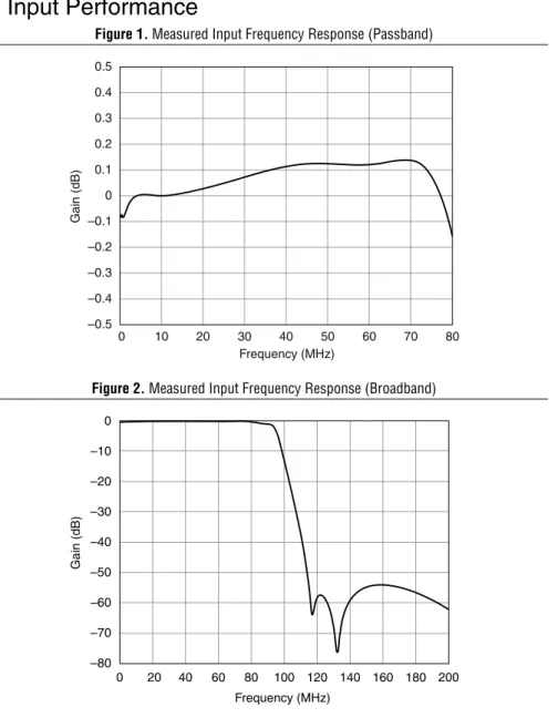
Passband flatness (referenced to 10 MHz) 250 kHz to 80 MHz
<+0.33 dB, -0.55 dB typical ...
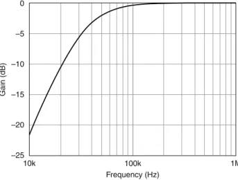
AC coupling cutoff frequency (-3 dB) 50 kHz typical ...
Input group delay variation 10 ns peak-to-peak typical, 250 kHz to 80 MHz ...
Stopband rejection >50 dB typical at 120 MHz, referenced to 10 MHz Channel-to-channel crosstalk ... <40 MHz <-70 dB typical ... 40 MHz to 80 MHz <-60 dB typical
IF Input Performance
Figure 1. Measured Input Frequency Response (Passband)
–0.2 –0.3 –0.4 –0.5 0.1 0.2 0.3 0.5 0.4 0 –0.1 0 10 20 30 40 50 70 80 Frequency (MHz) Gain (dB) 60
Figure 2. Measured Input Frequency Response (Broadband)
–40 –50 –60 –80 –70 –10 0 –20 –30 0 20 40 60 80 100 120 140 160 180 200 Frequency (MHz) Gain (dB)
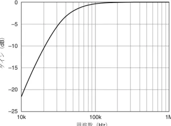
Figure 3. Measured Input Frequency Response (Low Frequency) –20 –25 –5 0 –10 –15 10k 100k 1M Frequency (Hz) Gain (dB)
Figure 4. Measured Phase Noise (Carrier Frequency = 62.922 MHz)
–110 –120 –130 –140 –150 –60 –70 –80 –90 –100 10 100 1k 10k 100k 1M 10M Offset Frequency (Hz) Phase Noise (dBc/Hz)
IF Input Spectral Characteristics
...IF Input Spectral Characteristics Performance
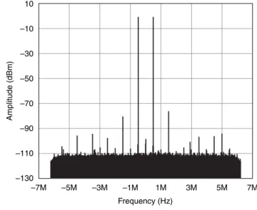
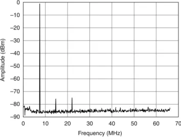
Figure 5. Measured Analog Input Two-Tone Intermodulation Distortion (IMD)
(Center frequency at 70 MHz, Two Carriers at 70 MHz ± 0.5 MHz, 0 dBm each)
–70 –90 –110 –130 –10 10 –30 –50 –7M –5M –3M –1M 1M 3M 5M 7M Frequency (Hz) Amplitude (dBm)
Digital Downconverter Characteristics
...Number of channels Up to 6 per ADC channel ...
DDC resolution 16 bits for both I and Q data ...
Decimation1 ÷4 to ÷4,096
...
Tuning resolution ADC clock/232
Related Information
Internal Timebase on page 10
1 Higher decimation is possible using LabVIEW FPGA, depending on performance requirements.
Digital Downconverter (DDC) Performance
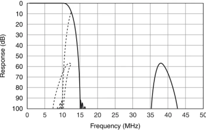
Figure 6. DDC Filter Performance, 20 MHz Span (Solid) and Aliasing After Decimation (Dashed) 0 10 20 30 40 50 60 70 80 90 100 Response (dB) Frequency (MHz) 0 5 10 15 20 25 30 35 40 45 50
Figure 7. DDC Filter Performance, 10 MHz Span
0 5 10 15 20 25 30 35 40 45 50 Frequency (MHz) Response (dB) –50 –60 –70 –80 –90 –100 0 –10 10 –20 –30 –40
Sample DDC filter performance plots use NI-5640R 1.3 instrument driver library example filter designs. The dark lines in the above figures show the true response of the digital filter in the DDC. The dashed lines show the effect of aliasing after decimation. Notice that for a 10 MHz span, the DDC filter aliasing artifacts have virtually no impact; whereas for a full 20 MHz span, signals at frequency offsets near ±40 MHz can alias back up to -66 dBc within the ±10 MHz passband near the band edges.
IF Output
...
Number of channels 2
...
DAC resolution 14 bits
...
Sample rate 30 MS/s to 200 MS/s
...
Output coupling AC-coupled
...
Output impedance 50 Ω nominal
...
Output return loss <-15 dB typical, 250 kHz to 80 MHz ...
Maximum DC bias voltage without damage 10 V ...
Average noise density -153 dBm/Hz typical Signal-to-noise ratio
...
+2 dBm output level >69 dB typical ...
-4 dBm output level >64 dB typical Full-scale output range2
...
CIC and inverse sync ON -4 dBm peak at 10 MHz ± 1 dB typical (0.4 Vpeak-peaksine, 0.14 VRMS)
...
Filters off, uncompensated +2 dBm peak at 10 MHz ± 1 dB typical (0.8 Vpeak-peaksine, 0.28 VRMS)
...
Output protection Indefinite duration short to ground ...
Maximum reverse power without damage +24 dBm peak (10 Vpeak-peak, 3.5 VRMS)
... Passband flatness
(referenced at 10 MHz)
<±1 dB typical, 250 kHz to 80 MHz
(with CIC and sync compensation filter engaged) ...
AC coupling cutoff frequency (-3 dB) 50 kHz typical Channel-to-channel crosstalk
...
<40 MHz <-70 dB typical
...
≥40 MHz to 80 MHz <-60 dB typical
2 Instrument driver enables CIC and inverse sync compensation by default, and the compensation cannot be bypassed.
IF Output Performance
Figure 8. Measured Analog Output Passband Flatness (Referenced to 10 MHz)
0 –0.2 –0.3 –0.4 –0.5 0.1 0.2 0.3 0.5 0.4 –0.1 0 10 20 30 40 50 70 80 Frequency (MHz) Gain (dB) 60
IF Output Spectral Characteristics Performance
Figure 9. Measured Analog Output Single-Tone Distortion(Carrier Frequency = 7.36 MHz, Inverse Sync Filter OFF, Output Amplitude = -3 dBFS)
0 –40 –50 –60 –90 –70 –80 –10 –20 –30 0 10 20 30 40 50 60 70 Frequency (MHz) Amplitude (dBm)
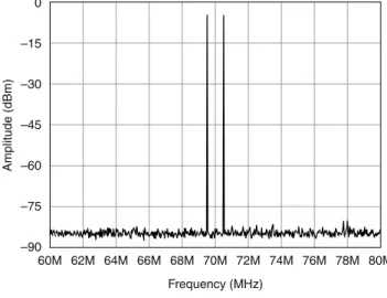
Figure 10. Measured Analog Output Two-Tone IMD
(Center Frequency at 70 MHz, Carriers at 70 MHz ± 0.5 MHz, -5 dBm Each, Inverse Sync Filter ON)
–60 –75 –90 –15 0 –30 –45 60M 62M 64M 66M 68M 70M 72M 74M 76M 78M 80M Frequency (MHz) Amplitude (dBm)
Digital Upconverter Characteristics
...Number of channels 1 per DAC channel ...
DUC resolution 14 bits for both I and Q data ...
Interpolation 4x to 252x
...
Modulation bandwidth Up to 40 MHz ...
Tuning resolution DAC clock/232. (For example, a 200 MHz
clock results in a 46.6 mHz tuning resolution.)
System Level Performance
System Level Modulation Quality
...Conditions 8-QAM, symbol rate: 3.125 MHz, PRN 9 sequence, power: -5 dBm, filter alpha 0.22, filter length 128, root-raised cosine
Modulation error ratio (MER)3 ... 10 MHz carrier >57 dB typical ... 40 MHz carrier >54 dB typical ... 70 MHz carrier >46 dB typical
Data Transfer Rate
(Using NI PXIe-1062Q chassis, NI PXIe-8130 controller, single-threaded, half-duplex transfer; transfer rate is dependent upon controller and chassis hardware, software, and backplane usage.)
...
NI PXIe-5641R to host 120 MB/s typical ...
Host to NI PXIe-5641R 52 MB/s typical
Timebase System
Internal Timebase
...
Timebase frequency4 200 MHz ± 35 ppm, maximum
...
Minimum Sample Clock divisor 2 for ADC, 1 for DAC ...
Supported divisors 1, 2, 4, 8, and 16
External Clock/External Frequency Reference
...Impedance 50 Ω nominal, AC-coupled
Input amplitude range
...
Sine wave 0.63 Vpeak-peak to 2.8 Vpeak-peak (0 dBm to 13
dBm) ...
Square wave 0.25 Vpeak-peak to 2.8 Vpeak-peak
...
Maximum input level without damage +24 dBm (10 Vpeak-peak, 3.5 VRMS)
... Maximum PLL lock time 250 ms ...
External Reference Clock range5 1 MHz to 100 MHz in 1 MHz increments,
±100 ppm ...
External Sample Clock range6 30 MHz to 200 MHz
3 MER performance estimated using short (7.62 cm, or 3 in.) loopback cables from output to input. 4 Adjusted during calibration
5 The CLK IN connector on the NI PXIe-5641R can function as either a Reference Clock input or a Sample Clock input.
Trigger System
...
Modes Digital input, software
Sources
...
Using instrument driver TRIG or software ...
Using LabVIEW FPGA TRIG, RTSI <0..7> (mapped to PXIe_TRIG<0..7>), or software Slope
... Using instrument driver Rising ...
Using LabVIEW FPGA Rising or falling
External Trigger Channel (TRIG)
...Impedance 10 kΩ nominal, DC-coupled
...
Range 0 V to 3.3 V typical, 5 V tolerant
...
VIH 2.2 V typical
...
VIL 0.95 V typical
...
Overvoltage protection -3.5 V to +8 V continuous ...
Maximum trigger frequency <10 MHz typical, system dependent ...
Input rise/fall time <10 ns/V typical
AUX I/O Connector
... Number of digital lines 7 ...
I/O direction Pin-configurable
...
Input voltage range 0 V to 3.3 V typical, 5 V tolerant ... VIH 2.5 V typical ... VIL 1 V typical ... VOH 3.5 V typical, no load ... VOL 0.1 V typical, no load ... Overvoltage protection -0.5 to +5.5 V
6 The CLK IN connector on the NI PXIe-5641R can function as either a Reference Clock input or a Sample Clock input.
...
Output type 3.3 V CMOS
...
Output current ±24 mA
...
Output impedance 56 Ω
...
+5 V power output voltage 5 V ± 10% ...
+5 V power output current 500 mA, ±150 mA typical, electronically fused
FPGA
...
Model Xilinx Virtex 5 SX95T
...
Logic cells 94,208
... Multipliers/DSP blocks (18 * 18) 640 ...
Block RAM 8,784 (kbits max)
Onboard DRAM
...
Memory size 128 MB
...
Theoretical maximum data rate 1,600 MB/s
Maximum Power Requirements
... +3.3 VDC 3 A ... +12 VDC 3 A ... Total power 38.25 WPhysical Characteristics
...Dimensions 3U, one slot, PXI Express module 21.6 cm * 2.0 cm * 13.0 cm (8.5 in * 0.8 in * 5.1 in) ...
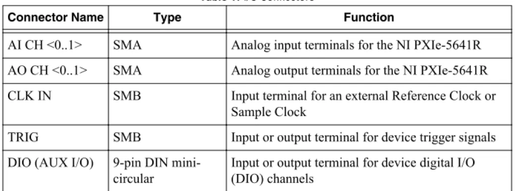
Table 1. I/O Connectors
Connector Name Type Function
AI CH <0..1> SMA Analog input terminals for the NI PXIe-5641R AO CH <0..1> SMA Analog output terminals for the NI PXIe-5641R CLK IN SMB Input terminal for an external Reference Clock or
Sample Clock
TRIG SMB Input or output terminal for device trigger signals DIO (AUX I/O) 9-pin DIN
mini-circular
Input or output terminal for device digital I/O (DIO) channels
Environment
...
Maximum altitude 2,000 m (at 25 °C ambient temperature) ...
Pollution Degree 2
Indoor use only.
Operating Environment
...Ambient temperature range 0 °C to 55 °C (Tested in accordance with IEC-60068-2-1 and IEC-60068-2-2.) ...
Relative humidity range 10% to 90%, noncondensing (Tested in accordance with IEC-60068-2-56.)
Storage Environment
...
Ambient temperature range -40 °C to 70 °C (Tested in accordance with IEC-60068-2-1 and IEC-60068-2-2.) ...
Relative humidity range 5% to 95%, noncondensing (Tested in accordance with IEC-60068-2-56.) ...
Operational shock 30 g peak, half-sine, 11 ms pulse (Tested in accordance with IEC-60068-2-27. Test profile developed in accordance with
Random vibration
...
Operating 5 Hz to 500 Hz, 0.3 grms
...
Nonoperating 5 Hz to 500 Hz, 2.4 grms (Tested in accordance
with IEC-60068-2-64. Nonoperating test profile exceeds the requirements of MIL-PRF-28800F, Class 3.)
Compliance and Certifications
Safety
This product is designed to meet the requirements of the following electrical equipment safety standards for measurement, control, and laboratory use:
• IEC 61010-1, EN 61010-1 • UL 61010-1, CSA 61010-1
Note For UL and other safety certifications, refer to the product label or the Online Product Certification section.
Electromagnetic Compatibility
This product meets the requirements of the following EMC standards for electrical equipment for measurement, control, and laboratory use:
• EN 61326-1 (IEC 61326-1): Class A emissions; Basic immunity • EN 55011 (CISPR 11): Group 1, Class A emissions
• AS/NZS CISPR 11: Group 1, Class A emissions • FCC 47 CFR Part 15B: Class A emissions • ICES-001: Class A emissions
Note In the United States (per FCC 47 CFR), Class A equipment is intended for
use in commercial, light-industrial, and heavy-industrial locations. In Europe, Canada, Australia, and New Zealand (per CISPR 11), Class A equipment is intended for use only in heavy-industrial locations.
Note Group 1 equipment (per CISPR 11) is any industrial, scientific, or medical
equipment that does not intentionally generate radio frequency energy for the treatment of material or inspection/analysis purposes.
Note For EMC declarations, certifications, and additional information, refer to the
Online Product Certification section.
CE Compliance
• 2006/95/EC; Low-Voltage Directive (safety)
• 2004/108/EC; Electromagnetic Compatibility Directive (EMC)
Online Product Certification
To obtain product certifications and the DoC for this product, visit ni.com/certification, search by model number or product line, and click the appropriate link in the Certification column.
Environmental Management
NI is committed to designing and manufacturing products in an environmentally responsible manner. NI recognizes that eliminating certain hazardous substances from our products is beneficial not only to the environment but also to NI customers.
For additional environmental information, refer to the Minimize Our Environmental Impact web page at ni.com/environment. This page contains the environmental regulations and directives with which NI complies, as well as other environmental information not included in this document.
Waste Electrical and Electronic Equipment (WEEE)
EU Customers At the end of the product life cycle, all products must be sent to a
WEEE recycling center. For more information about WEEE recycling centers, National Instruments WEEE initiatives, and compliance with
WEEE Directive 2002/96/EC on Waste Electrical and Electronic Equipment, visit
ni.com/environment/weee.htm.
电子信息产品污染控制管理办法(中国
RoHS)
中国客户 National Instruments 符合中国电子信息产品中限制使用某些有害物 质指令(RoHS)。关于 National Instruments 中国 RoHS 合规性信息,请登录 ni.com/environment/rohs_china。(For information about China RoHS compliance, go to ni.com/environment/rohs_china.)
Refer to the NI Trademarks and Logo Guidelines at ni.com/trademarks for information on National Instruments trademarks. Other product and company names mentioned herein are trademarks or trade names of their respective companies. For patents covering National Instruments products/technology, refer to the appropriate location: Help»Patents in your software, the
patents.txt file on your media, or the National Instruments Patent Notice at ni.com/patents. You can find information about end-user license agreements (EULAs) and third-party legal notices in the readme file for your NI product. Refer to the Export Compliance Information at ni.com/legal/export-compliance for the National Instruments global trade compliance policy and how to obtain relevant HTS codes, ECCNs, and other import/export data.
デバイス仕様
NI PXIe-5641R
再構成可能 IF トランシーバ
このドキュメントには、 NI PXIe-5641R 再構成可能 IF トランシーバの仕様が記載されて います。仕様は、特に注釈のない限り、設計により、および以下の条件下において保 証されています。 • 10分のウォームアップ時間 • 一定に維持されたキャリブレーション間隔 • シャーシのファンの速度を HIGH に設定 最大値および最小値として示されている仕様の値は、特に指定がない限り、0~55℃の 周囲温度範囲内で使用した場合の、保証済みでトレーサブルな製品性能を記載してい ます。 標準値は、保証範囲外での使用における有用な製品性能を表しますが、これには測定 の不確定性やドリフトに対するガードバンドは含まれていません。標準値は工場から 出荷されたすべてのユニットで確認されるとは限りません。特に指定がない限り、標 準値は、この製品の開発時または製造時の測定値に基づいて、25±10℃(信頼水準 90%)の周囲温度範囲内で使用した場合の、ユニットの予想性能を記載しています。 公称値(または補足情報)は、仕様または標準値に記載されていない予想性能を含む、 製品の有用な追加情報を記載しています。公称値は保証範囲外です。 仕様は事前の通知なしに変更されることがあります。最新の仕様および製品のドキュ メントについては、ni.com/manualsを参照してください。 NI 5641R のドキュメントにアクセスするには、 スタート→すべてのプログラム→ National Instruments→NI-5640R→ドキュメント を参照してください。 注意 このドキュメントに記載されている以外の方法で NI PXIe-5641R を使 用しないでください。製品の使用を誤ると危険です。また、破損した製品を 使用した場合には、従来の安全性を保証することはできません。製品が破損 している場合は、ナショナルインスツルメンツまでお問い合わせください。IF
入力
... チャンネル数 2 ... ADC分解能 14ビット ... サンプルレート 30 MS/s~100 MS/s ... フルスケール入力範囲 +8.5 dBmピーク(10 MHz 時)± 1 dB(標 準)(1.7 Vpeak–peak正弦波、0.60 VRMS) ... 最大入力レベル(無破損) +24 dBmピーク (10Vpeak–peak正弦波、3.5 VRMS) ... 入力カプリング AC ... 入力インピーダンス 50 Ω(公称) ... 入力反射減衰量 <-15 dB(標準)、250 kHz~80 MHz ... 最大 DC 入力電圧(無破損) 10 V ... 平均ノイズ密度 -143 dBm/Hz(標準) ... SN比 >76 dB(標準) (68 MHz トーン時-1 dBfs、帯域幅 = 10 MHz) ... 最大即時帯域幅 20 MHz(デジタルダウンコンバータによる 制限あり) ... パスバンドフラットネス (10 MHz 基準) 250 kHz~80 MHz <+0.33 dB、-0.55 dB(標準) ... ACカプリングカットオフ周波数(-3 dB) 50 kHz(標準) ... 入力群遅延特性 10 ns(ピーク間、標準)、 250 kHz~80 MHz ... ストップバンド除去 >50 dB(120 MHz 時標準)(10 MHz 基準) チャンネル間クロストーク ... <40 MHz <-70 dB(標準) ... 40 MHz~80 MHz <-60 dB(標準)IF
入力性能
図 1 測定された入力周波数応答(パスバンド) –0.2 –0.3 –0.4 –0.5 0.1 0.2 0.3 0.5 0.4 0 –0.1 0 10 20 30 40 50 70 80 周波数(MHz) ゲイン( dB ) 60 図 2 測定された入力周波数応答(ブロードバンド) –40 –50 –60 –80 –70 –10 0 –20 –30 0 20 40 60 80 100 120 140 160 180 200 周波数(MHz) ゲイン( dB )図 3 測定された入力周波数応答(低周波) –20 –25 –5 0 –10 –15 10k 100k 1M 周波数(Hz) ゲイン( dB ) 図 4 測定された位相ノイズ(搬送波周波数 = 62.922 MHz) –110 –120 –130 –140 –150 –60 –70 –80 –90 –100 10 100 1k 10k 100k 1M 10M オフセット周波数(Hz) 位相ノイズ( dBc/Hz )
IF
入力スペクトル特性
... 3次インタセプト(TOI) +38 dBm(標準)IF
入力スペクトル特性
図 5 測定されたアナログ入力 2 トーン相互変調歪み(IMD)(中心周波数 70 MHz、70 MHz ±0.5 MHz、各 0 dBm の 2 つの搬送波) –70 –90 –110 –130 –10 10 –30 –50 –7M –5M –3M –1M 1M 3M 5M 7M 周波数(Hz) 振幅( dBm )デジタルダウンコンバータ特性
... チャンネル数 最大 6(ADC チャンネルあたり) ... DDC分解能 16ビット、I データおよび Q データの両方 に対して ... デシメーション1 ÷4~÷4,096 ... 調整分解能 ADCクロック/232 関連情報 内部タイムベース(10 ページ) 1 パフォーマンス要件により、LabVIEW FPGA を使用してより高いデシメーション が可能です。デジタルダウンコンバータ(DDC)性能
図 6 DDC フィルタ性能、20 MHz スパン(実線)およびデシメーション後のエイリアシ ング(点線) 0 10 20 30 40 50 60 70 80 90 100 応答( dB ) 周波数(MHz) 0 5 10 15 20 25 30 35 40 45 50 図 7 DDC フィルタ性能、10 MHz スパン 0 5 10 15 20 25 30 35 40 45 50 周波数(MHz) 応答( dB ) –50 –60 –70 –80 –90 –100 0 –10 10 –20 –30 –40 NI-5640R 1.3計測器ドライバライブラリのサンプルフィルタ設計を使用したサンプル DDCフィルタ性能のプロットを示します。上図の実線は DDC におけるデジタルフィ ルタの正確な応答を示しています。また、各グラフの点線はデシメーション後のエイ リアシングの影響を示しています。10 MHz スパンでは DDC フィルタのエイリアシン グアーチファクトは実質的に影響がありませんが、全 20 MHz スパンでは±40 MHz 近辺 の周波数オフセット信号は帯域幅の端近くの±10 MHz パスバンド内で最大-66 dBc の エイリアシングが発生する場合があります。IF
出力
... チャンネル数 2 ... DAC分解能 14ビット ... サンプルレート 30 MS/s~200 MS/s ... 出力カプリング ACカプリング ... 出力インピーダンス 50 Ω(公称) ... 出力反射減衰量 <-15 dB(標準)、250 kHz~80 MHz ... 最大 DC バイアス電圧(無破損) 10 V ... 平均ノイズ密度 -153 dBm/Hz(標準) SN比 ... +2 dBm出力レベル >69 dB(標準) ... -4 dBm出力レベル >64 dB(標準) フルスケール出力範囲2 ... CICおよび逆 sync 有効時 -4 dBmピーク(10 MHz 時)± 1 dB(標準) (0.4 Vpeak–peak正弦波、0.14 VRMS) ... フィルタ無効、補正無効時 +2 dBmピーク(10 MHz 時)± 1 dB(標準) (0.8 Vpeak–peak正弦波、0.28 VRMS) ... 出力保護 無限継続時間グランド短絡 ... 最大逆電力(無破損) +24 dBmピーク(10 Vpeak–peak、3.5 VRMS) ... パスバンドフラットネス (10 kHz 基準) (CIC および sync 補正フィルタ有効時)<±1 dB(標準)、250 kHz~80 MHz ... ACカプリングカットオフ周波数(-3 dB) 50 kHz(標準) チャンネル間クロストーク ... <40 MHz <-70 dB(標準) ... ≥40 MHz~80 MHz <-60 dB(標準) 2 計測器ドライバが CIC および逆 sync 補正をデフォルトで有効にするため、補正はバイパ スできません。IF
出力性能
図 8 測定されたアナログ出力パスバンドフラットネス(10 MHz 基準) 0 –0.2 –0.3 –0.4 –0.5 0.1 0.2 0.3 0.5 0.4 –0.1 0 10 20 30 40 50 70 80 周波数(MHz) ゲイン( dB ) 60IF
出力スペクトル特性
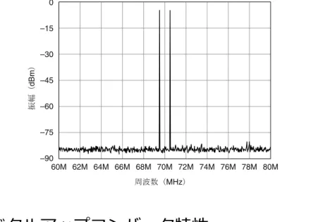
図 9 測定されたアナログ出力シングルトーン歪み (搬送波周波数 = 7.36 MHz、逆同期フィルタ無効、出力振幅 = -3 dBFS) 0 –40 –50 –60 –90 –70 –80 –10 –20 –30 0 10 20 30 40 50 60 70 周波数(MHz) 振幅( dBm )図 10 測定されたアナログ出力 2 トーン IMD(70 MHz の中心周波数、70 MHz ± 0.5 MHz、 各-5 dBm の搬送波、逆同期フィルタ有効) –60 –75 –90 –15 0 –30 –45 60M 62M 64M 66M 68M 70M 72M 74M 76M 78M 80M 周波数(MHz) 振幅( dBm )
デジタルアップコンバータ特性
... チャンネル数 1(DAC チャンネルあたり) ... DUC分解能 14ビット、I データおよび Q データの両方 に対して ... 補間 4x~252x ... 変調帯域幅 最大 40 MHz ... 調整分解能 DACクロック/232(例: 200 MHz クロックは 46.6 mHz調整分解能となります。)システムレベル性能
システムレベル変調品質
... 条件 8-QAM、シンボルレート: 3.125 MHz、PRN 9 シーケンス、電力: -5 dBm、フィルタアル ファ 0.22、フィルタ長 128、平方根二乗余 弦変調誤差比(MER)3 ... 10 MHz搬送波 >57 dB(標準) ... 40 MHz搬送波 >54 dB(標準) ... 70 MHz搬送波 >46 dB(標準)
データ転送レート
(NI PXIe-1062Q シャーシ、NI PXIe-8130 コントローラを使用した、シングルスレッド、 半二重転送。転送レートは、コントローラおよびシャーシのハードウェア、ソフトウェ ア、およびバックプレーンの使用に依存します。) ... NI PXIe-5641R ~ホスト 120 MB/s(標準) ... ホスト~ NI PXIe-5641R 52 MB/s(標準)
タイムベースシステム
内部タイムベース
... タイムベース周波数4 200 MHz ± 35 ppm(最大) ... 最小サンプルクロック分周率 2(ADC に対して)、1(DAC に対して) ... サポートされる分周率 1、2、4、8、および 16外部クロック/外部周波数基準
... インピーダンス 50Ω(公称)、AC カプリング 入力振幅範囲 ... 正弦波 0.63 Vpeak-peak~2.8 Vpeak-peak(0 dBm~13 dBm) ... 方形波 0.25 Vpeak-peak~2.8 Vpeak-peak ... 最大入力レベル(無破損) +24 dBm(10 Vpeak–peak、3.5 VRMS) ... 最大 PLL ロック時間 250 ms 3 MERのパフォーマンスは、出力間に 7.62 cm(3 インチ)の短いループバックケーブルを 使用した推測値です。 4 キャリブレーション中に調整。... 外部基準クロック範囲5 1 MHz~100 MHz(1 MHz 間隔)、±100 ppm ... 外部サンプルクロック範囲6 30 MHz~200 MHz
トリガシステム
... モード デジタル入力、ソフトウェア ソース ... 計測器ドライバ使用時 TRIGまたはソフトウェア ...LabVIEW FPGA使用時 TRIG、RTSI <0..7> (PXIe_TRIG<0..7>にマッピ ング)、ソフトウェア スロープ ... 計測器ドライバ使用時 立ち上がり ... LabVIEW FPGA使用時 立ち上がりまたは立ち下がり
外部トリガチャンネル(TRIG)
... インピーダンス 10 kΩ(公称)、DC カプリング ... 範囲 0~3.3 V(標準)、5 V(許容) ... VIH 2.2 V(標準) ... VIL 0.95 V(標準) ... 過電圧保護 -3.5~+8 V(連続) ... 最大トリガ周波数 <10 MHz(標準)、システム依存 ... 入力立ち上がり/立ち下がり時間 <10 ns/V(標準)AUX I/O
コネクタ
... デジタルライン数 7 ... 入出力の方向 ピンにより構成可能 ... 入力電圧範囲 0~3.3 V(標準)、5 V(許容) 5 NI PXIe-5641R の CLK IN コネクタは、基準クロック入力またはサンプルクロック 入力のいずれかとして機能します。 6 NI PXIe-5641R の CLK IN コネクタは、基準クロック入力またはサンプルクロック 入力のいずれかとして機能します。... VIH 2.5 V(標準) ... VIL 1 V(標準) ... VOH 3.5 V(標準)、無負荷 ... VOL 0.1 V(標準)、無負荷 ... 過電圧保護 -0.5~+5.5 V ... 出力タイプ 3.3 V CMOS ... 出力電流 ±24 mA ... 出力インピーダンス 56 Ω ... +5 V電源出力電圧 5 V±10% ... +5 V電源出力電流 500 mA、±150 mA(標準)、電気ヒューズ付
FPGA
... 型番 Xilinx Virtex 5 SX95T ... 論理セル数 94,208 ... 乗数/DSP ブロック(18 * 18) 640 ... ブロック RAM 8,784(k ビット最大)オンボード DRAM
... メモリサイズ 128 MB ... 理論的最大データレート 1,600 MB/s最大所要電力
... +3.3 VDC 3 A ... +12 VDC 3 A ... 合計電力 38.25 W物理特性
... 外形寸法 3U、1 スロット、PXI Express モジュール 21.6 x 2.0 x 13.0 cm(8.5 x 0.8 x 5.1 in.) ... 重量 397 g(13.4 oz) 表 1 I/O コネクタ コネクタ名 タイプ 機能 AI CH <0..1> SMA NI PXIe-5641R のアナログ入力端子 AO CH <0..1> SMA NI PXIe-5641R のアナログ出力端子 CLK IN SMB 外部基準クロックまたはサンプルクロック用入力 端子 TRIG SMB デバイスのトリガ信号用入力または出力端子DIO(AUX I/O) 9 ピン DIN ミ
ニサーキュラ デバイスのデジタル I/O(DIO)チャンネル用入力または出力端子
環境
... 最大使用高度 2,000 m(周囲温度 25℃時) ... 汚染度 2 室内使用のみ。動作環境
... 周囲温度範囲 0℃~55℃(IEC-60068-2-1 および IEC-60068-2-2に準拠して試験済み。) ... 相対湿度範囲 10~90%、結露なきこと(IEC-60068-2-56 に 従って試験済み。)保管環境
... 周囲温度範囲 -40℃~70℃(IEC-60068-2-1 および IEC-60068-2-2に準拠して試験済み。) ... 相対湿度範囲 5~95%、結露なきこと(IEC-60068-2-56 に 従って試験済み。) ... 動作時衝撃 最大 30 g(半正弦波)、11 ms パルス (IEC-60068-2-27 に準拠して試験済み。MIL-PRF-28800Fに準拠してテストプロファイル を確立。) ランダム振動 ... 動作時 5~500 Hz、0.3 grms ... 非動作時 5~500 Hz、2.4 grms(IEC-60068-2-64 に準拠 して試験済み。非動作時のテストプロファ イルは MIL-PRF-28800F、Class 3 の要件を上 回る。)認可および準拠
安全性
この製品は、計測、制御、実験に使用される電気装置に関する以下の規格要件を満た すように設計されています。 • IEC 61010-1、EN 61010-1 • UL 61010-1、CSA 61010-1 メモ UL およびその他の安全保証については、製品ラベルまたは「オンライ ン製品認証」セクションを参照してください。電磁両立性
この製品は、計測、制御、実験に使用される電気装置に関する以下の EMC 規格の必要 条件を満たします。 • EN 61326-1 (IEC 61326-1): Class A エミッション、基本イミュニティ • EN 55011 (CISPR 11): Group 1、Class A エミッション• FCC 47 CFR Part 15B: Class Aエミッション • ICES-001: Class Aエミッション メモ 米国では(FCC 47 CFR に従って)、Class A 機器は商業、軽工業、およ び重工業の設備内での使用を目的としています。欧州、カナダ、オーストラ リア、およびニュージーランドでは(CISPR 11 に従って)、Class A 機器は重 工業の設備内のみでの使用を目的としています。 メモ Group 1 機器とは(CISPR 11 に従って)材料の処理または検査/分析の 目的で無線周波数エネルギーを意図的に生成しない工業用、科学、または医 療向け機器のことです。 メモ EMC 宣言および認証については、「オンライン製品認証」セクション を参照してください。
CE
マーク準拠
この製品は、該当する EC 理事会指令による基本的要件に適合しています。 • 2006/95/EC、低電圧指令(安全性) • 2004/108/EC、電磁両立性指令(EMC)オンライン製品認証
この製品の製品認証および適合宣言を入手するには、ni.com/certificationにアクセス して型番または製品ラインで検索し、保証の欄の該当するリンクをクリックしてくだ さい。環境管理
ナショナルインスツルメンツは、環境に優しい製品の設計および製造に努めています。 NIは、製品から特定の有害物質を除外することが、環境のみならず NI のお客様にとっ て有益であると考えています。環境に関する詳細は、ni.com/environmentからアクセス可能な「Minimize Our Environmental Impact」ページ(英語)を参照してください。このページには、ナショ ナルインスツルメンツが準拠する環境規制および指令、およびこのドキュメントに含 まれていないその他の環境に関する情報が記載されています。
廃電気電子機器(WEEE)
欧州のお客様へ 製品寿命を過ぎたすべての製品は、必ず WEEE リサイクル センターへ送付してください。WEEE リサイクルセンターおよびナショナル インスツルメンツの WEEE への取り組み、および廃電気電子機器のWEEE指令 2002/96/EC 準拠については、ni.com/environment/weee(英語) を参照してください。
电子信息产品污染控制管理办法(中国
RoHS)
中国客户 National Instruments 符合中国电子信息产品中限制使用某些有害物 质指令(RoHS)。关于 National Instruments 中国 RoHS 合规性信息,请登录 ni.com/environment/rohs_china。(For information about China RoHS compliance, go to ni.com/environment/rohs_china.)
National Instrumentsの商標については、ni.com/trademarksに掲載されている「NI Trademarks and Logo Guidelines」をご覧 ください。本文書中に記載されたその他の製品名および企業名は、それぞれの企業の商標または商号です。National Instruments の製品/技術を保護する特許については、ソフトウェアで参照できる特許情報(ヘルプ→特許情報)、メディアに含まれている patents.txtファイル、またはni.com/patentsからアクセスできる National Instruments Patent Notice(英語)のうち、該当す るリソースから参照してください。エンドユーザ使用許諾契約(EULA)および他社製品の法的注意事項はご使用の NI 製品の Readmeファイルにあります。ナショナルインスツルメンツの輸出関連法規遵守に対する方針について、また必要な HTS コー ド、ECCN、その他のインポート/エクスポートデータを取得する方法については、「輸出関連法規の遵守に関する情報」(ni.com/ legal/export-compliance)を参照してください。