Negligible‐Pb‐Waste and Upscalable
Perovskite Deposition Technology for High‐
Operational‐Stability Perovskite Solar Modules
Author Yan Jiang, Mikas Remeika, Zhanhao Hu, Emilio J. Juarez‐Perez, Longbin Qiu, Zonghao Liu, Taehoon Kim, Luis K. Ono, Dae‐Yong Son, Zafer Hawash, Matthew R. Leyden, Zhifang Wu,
Lingqiang Meng, Jinsong Hu, Yabing Qi journal or
publication title
Advanced Energy Materials
volume 9
number 13
page range 1803047
year 2019‑02‑14
Publisher John Wiley and Sons
Rights (C) 2019 WILEY‐VCH Verlag GmbH & Co. KGaA, Weinheim
This is the peer reviewed version of the
following article: Jiang, Y., Remeika, M., Hu, Z., Juarez‐Perez, E. J., Qiu, L., Liu, Z., Kim, T., Ono, L. K., Son, D.‐Y., Hawash, Z., Leyden, M. R., Wu, Z., Meng, L., Hu, J., Qi, Y. B., Adv. Energy Mater. 2019, 9, 1803047, which has been published in final form at https://doi.org/10.1002/aenm.201803047. This article may be used for non‑commercial
purposes in accordance with Wiley Terms and Conditions for Use of Self‑Archived Versions.
Author's flag author
URL http://id.nii.ac.jp/1394/00000983/
doi: info:doi/10.1002/aenm.201803047
1 DOI: 10.1002/ ((please add manuscript number)) 1
Full Paper 2
3 4
Negligible-Pb-Waste and Upscalable Perovskite Deposition Technology for High 5
Operational-Stability Perovskite Solar Modules 6
7
Yan Jiang, Mikas Remeika, Zhanhao Hu, Emilio J. Juarez-Perez, Longbin Qiu, Zonghao Liu, Taehoon Kim, Luis
8
K. Ono, Dae-Yong Son, Zafer Hawash, Matthew R. Leyden, Zhifang Wu, Lingqiang Meng, Jinsong Hu, and Yabing
9 10 Qi*
11
Dr. Y, Jiang, Dr. M. Remeika, Dr. Z. Hu, Dr. E. J. Juarez-Perez, Dr. L. Qiu, Dr. Z. Liu, Dr. T.
12
Kim, Dr. L. K. Ono, Dr. D. Son, Dr. Z. Hawash, Dr. M. R. Leyden, Dr. Z. Wu, Dr. L. Meng, 13
Prof. Y. B. Qi 14
Energy Materials and Surface Sciences Unit (EMSSU) Okinawa Institute of Science and 15
Technology Graduate University (OIST) 1919-1 Tancha, Onna-son, Kunigami-gun, Okinawa 16
904-0495, Japan 17
*E-mail: [email protected] 18
Prof. J. Hu 19
National Research Center for Molecular Sciences, Key Laboratory of Molecular Nanostructure 20
and Nanotechnology, Institute of Chemistry, Chinese Academy of Sciences, Beijing 100190, P.
21
R. China 22
23 24
Keywords: perovskite, solar module, upscalable, lead waste, stability 25
26 27
Abstract:
28
We report an upscalable perovskite film deposition method combining raster ultrasonic spray 29
(RUS) coating and chemical vapor deposition (CVD). Our method overcomes the coating size 30
limitation of the existing stationary spray, single-pass spray and spin-coating methods. In 31
contrast with the spin-coating method (>90% Pb waste), negligible Pb waste during PbI2
32
deposition makes this method more environmentally friendly. Outstanding film uniformity 33
across the entire area of 5 cm 5 cm is confirmed by both large area compatible characterization 34
methods (electroluminescence and scattered light imaging) and local characterization methods 35
(AFM, SEM, photoluminescence mapping, UV-vis and XRD measurements on multiple sample 36
locations), resulting in low solar cell performance decrease upon increasing device area. With 37
the FAPb(I0.85Br0.15)3 perovskite layer deposited by this method, champion solar modules show 38
a power conversion efficiency of 14.7% on an active area of 12.0 cm2 and an outstanding shelf 39
2
stability (only 3.6% relative PCE decay after 3600 h aging). Under continuous operation (1 Sun 1
light illumination, maximum power point condition, dry N2 atmosphere with <5% relative 2
humidity, no encapsulation) our devices show high light-soaking stability corresponding to an 3
average T80 lifetime of 535 h on the small area solar cells and 388 h on the solar module.
4 5
Introduction 6
Over the past few years, there have been unprecedented advances in solar cells using metal 7
halide perovskite materials as light absorbers.1-3 A record power conversion efficiency (PCE) 8
of 23.3% has been certified, already surpassing the well-established commercial photovoltaic 9
technologies e.g., multi-crystalline silicon (22.3%), thin film CIGS (22.6%) and CdTe 10
(22.1%).4 Substantial efforts have also been made to solve other potential issues that may limit 11
the commercialization of this new technology. Less toxic elements (e.g., Sn2+, Bi3+, Ag1+, Sb3+) 12
are being tested to replace Pb2+, and PCE has reached 9%.5-12 Device stability is significantly 13
improved by optimizing the device structure,13-17 perovskite composition18 and deposition 14
technologies19-21. Research focus is now shifting to development of reliable perovskite 15
deposition technologies that would allow mass production in industry. To manufacture products 16
with commercially viable module size and yield, the factors that are often ignored in making 17
small-size cells in research labs can have a strong impact on levelized cost of electricity (LCOE) 18
and must be considered.22-25 These factors include (i) solar cell PCE should be maintained or 19
only decrease slightly upon increasing the active area from the small solar cell scale (active area 20
~ 0.1 cm2) towards the solar module scale (> active area ~ 10 cm2); (ii) Pb waste should be 21
minimized during the deposition process; (iii) the perovskite film deposition methods should 22
be transferable to industry.
23
Considering these factors, the methods developed in research labs may not be all suitable for 24
mass production. For example, most high-performing perovskite solar cells (PCE >20%) are 25
prepared by the anti-solvent based spin-coating method on small active areas (~ 0.1 cm2).
26
3
However film uniformity becomes significantly poorer upon increasing the active area to a 1
module scale due to the short precursor-processing window, leading to decreased device 2
performance and reproducibility.26-28 The inherently high Pb waste (> 90%) during the spin- 3
coating process,29 the associated cost of waste disposal, and the environmental impact also 4
make this method unsuitable. On the basis of these considerations, a series of scalable 5
perovskite deposition technologies are being developed including blade coating,26, 30-31 slot die 6
coating,32 spray coating,33-41 ink-jet printing,42 screen printing,43 chemical vapor deposition,44- 7
45 pressure-processed coating46 etc. However, devices based on these technologies typically 8
show much lower PCEs than those achieved in research labs on small size cells. Perovskite 9
films coated using these technologies are formed either by a one-step or a sequential conversion 10
process. Remeika et al. reported that the sequential conversion shows clear advantages over 11
one step deposition in the scalable technologies because functional film formation is separated 12
from film coating, allowing separate optimization of the two processes.29 13
In this work we develop an upscalable perovskite deposition technology combining raster 14
ultrasonic spray coating and chemical vapor deposition (RUS-CVD). FAPbIxBr3-x (FA = 15
formamidinium) perovskite films are deposited on FTO/ c-TiO2 substrates via a sequential 16
deposition method (Figure 1A). First, PbI2 films are prepared by raster ultrasonic spray-coating 17
(RUS) using a precursor solution containing a solvent mixture of DMF and DMSO (Figure 1B 18
and movie S1). PbI2 films are converted to FAPbIxBr3-x by CVD in the vapor of formamidinium 19
iodide (FAI), formamidinium bromide (FABr) and methylammonium chloride (MACl) (Figure 20
1C). The RUS-CVD method can address the aforementioned issues.
21
No limitation with respect to the substrate size. The spray coating methods can be divided 22
to three categories based on the operation modes: (a) Stationary spray with the spray head 23
completely fixed; (b) single-pass spray with the spray head only movable in one direction and 24
(c) raster spray with the spray head movable in both x and y directions. Almost all the reported 25
spray coating methods for perovskite deposition use either stationary spray38, 40 or single-pass 26
4
spray33, 34, 36. Attempting to coat two adjacent areas by stationary or single pass coating would 1
create an overlapped area dense with defects (see Supplementary Information for details of 2
raster coating vs. stationary or single-pass coating). Therefore although spray-coating is a 3
scalable deposition method, most of the reports are on the small cells (active area ≤ 1 cm2).
4
Uličná et al. reported a scalable perovskite deposition method using the raster spray-coating,35 5
but the active area of their devices was only 0.06 cm2. Hilt et al. reported a rapid spray plasma 6
processing method,39 but the authors only demonstrated the fabrication of small-area solar cells, 7
not solar modules. By controlling the precursor film drying process, we report a uniform PbI2
8
film deposition method based on a raster ultrasonic spray process on substrates with a size of 9
10 cm x 10 cm, which to our best knowledge, is the first report in the perovskite research 10
community to demonstrate continuously scalable spray coating with a pattern width not limited 11
by the size of the spray head. The subsequent conversion from PbI2 to perovskite via CVD has 12
also been shown to be scalable47-49 and with weak substrate size dependence44. The reaction 13
speed during the CVD step is slower than other open air processing methods, such as blade 14
coating. However, considering that a large number of large area substrates can be processed 15
simultaneously in a large CVD setup45, the deposition time per substrate is expected to be 16
substantially shorter.
17
Solar cell performance shows much lower substrate-size dependence than the mostly used 18
spin-coating method, owing to the high film uniformity and quality at large scale. (Figure 1D) 19
Low lead waste. PbI2 precursor utilization efficiency increases to almost 100% upon 20
increasing substrate size (78% for 1.5 cm x 1.5 cm, 92% for 5 cm x 5 cm, 96% for 10 cm x 10 21
cm, 99% for 30 cm x 30 cm, see the experimental section), significantly higher than the mostly 22
used spin-coating method (less than 10% Pb utilization at different substrate sizes). (Figure 1E) 23
Transferable to industry. Ultrasonic spray coating is widely used in industry for display and 24
lens coating, active layer and anti-reflection coating for solar cells, etc.50 CVD is also a mature 25
coating technology widely utilized in the thin film solar cell industry.47-49 26
5
It is important to note that widely employed single point local characterization methods that are 1
suitable for small solar cells (e.g., active area ~ 0.1 cm2) are no longer sufficient for 2
characterizing mini-modules (> 10 cm2 active area).39 To study thin film properties across large 3
area, UV-Vis spectroscopy, X-ray diffraction (XRD), atomic force microscopy (AFM), cross- 4
section scanning electron microscopy (SEM) and photoluminescence mapping are used to 5
characterize multiple locations on the 5 cm x 5 cm photoactive layers, to ensure the absorbance, 6
crystallinity and surface roughness are representative of the large area device. In addition, we 7
study film properties using large-area compatible characterization methods such as scattered 8
light intensity (SLI) imaging and electroluminescence (EL) imaging, which allow rapid 9
characterization of the entire 5 cm x 5 cm mini-modules and are also compatible with in-line 10
characterization in a production environment. With FAPb(I0.85Br0.15)3 perovskite layer 11
deposited by our method, perovskite mini-modules using the standard device architecture (i.e., 12
with a TiO2 electron transporting layer, a spiro-MeOTAD hole transporting layer, and a gold 13
electrode) show a champion module performance of 14.7% on an active area of 12.0 cm2. Under 14
continuous operation (constant 1 Sun light illumination, maximum power point, MPP, N2
15
atmosphere, <5% relative humidity, no encapsulation) devices show high stability 16
corresponding to an average T80 lifetime of 535 h on the small cells (based on the statistical 17
data of 4 small cells) and 388 h on the module.
18
Results and discussion 19
PbI2 deposition by RUS.
20
Several groups have reported using a co-solvent of DMF and DMSO mixture for the perovskite 21
precursor in the spin-coating process and the ratios are between 10:1 to 4:1 (V:V) to achieve 22
uniform perovskite deposition.18, 51 However, our initial results based on single-pass ultrasonic 23
spray (SUS)-coated PbI2 suggest that this optimized ratio for perovskite is not directly 24
applicable to spray-coating PbI2 due to the different crystallization dynamics.34 Generally, a 25
higher DMSO concentration leads to a longer evaporation time because of its higher boiling 26
6
point and higher solubility for PbI2 stemming from its higher coordination number, but a lower 1
viscosity. 52-54 Uniformity of the PbI2 layer changes substantially as we vary the ratio between 2
DMF and DMSO in the RUS process. The optimal PbI2 deposition by SUS is not suitable for 3
the RUS process. Therefore we optimize the DMF:DMSO ratio for PbI2 deposition via RUS 4
starting from 14:1 (volume ratio) according to our reported SUS method.34 Four types of solvent 5
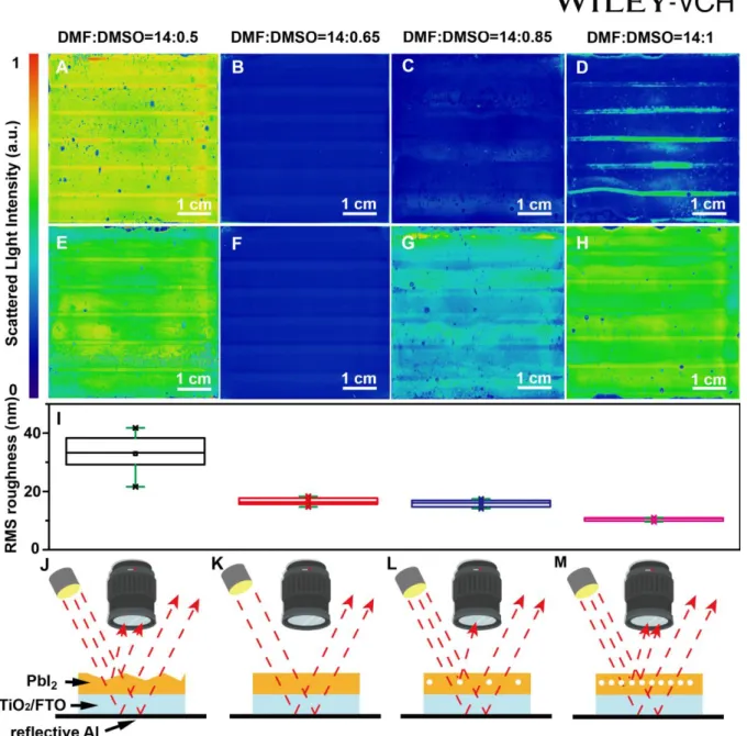
mixtures with the DMF:DMSO ratio varying from 14:0.5 to 14:1 are employed to dissolve PbI2. 6
SLI mapping measurements are performed on the entire 5 cm × 5 cm sprayed PbI2 precursor 7
and annealed films. Different SLI is either caused by different surface roughness or different 8
amount of micro cracks in the film bulk (see Supplemental Information for details on the SLI 9
mapping measurement). We observe that low DMSO concentration in the co-solvent, i.e., 10
(DMF : DMSO = 14 : 0.5) results in a PbI2 precursor film with high SLI that resembles the film 11
coated using pure DMF solvent (Figure 2A).32 The high SLI remains after the film is annealed 12
(Figure 2E). Medium DMSO concentration (DMF : DMSO = 14 : 0.65) results in translucent 13
PbI2 precursor films with low SLI (Figure 2B), which remains after annealing (Figure 2F). High 14
DMSO concentrations (DMF : DMSO = 14 : 0.85 and DMF : DMSO = 14 : 1) result in slightly 15
increased SLI again for the PbI2 precursor films (Figure 2C and 2D). The SLI increased strongly 16
after annealing (Figure 2G and 2H), due to formation of the internal cracks and voids caused 17
by evaporation of DMSO. 55 AFM measurements are carried out on 6 different locations of each 18
5 cm × 5 cm PbI2 film to study the surface roughness. RMS roughness decreases drastically 19
with DMSO concentration increasing from low (DMF : DMSO = 14 : 0.5) to medium (DMF : 20
DMSO = 14 : 0.65) and decreases slightly with further increasing the DMSO concentration 21
(DMF : DMSO = 14 : 0.85 and DMF : DMSO = 14 : 1) (Figure 2I and Figure S1). We interpret 22
the SLI and AFM data as follows. A low DMSO concentration (DMF : DMSO = 14 : 0.5) in 23
the solvent mixture results in a dense PbI2 film with rough surface. While high DMSO 24
concentrations (DMF : DMSO = 14 : 0.85 and DMF : DMSO = 14 : 1) result in a smooth film 25
surface but with a large amount of internal cracks and voids (Figure 2J-M). A medium DMSO 26
7
concentration results in a smooth PbI2 film with negligible internal cracks and voids. A rough 1
PbI2 film will convert to a rough perovskite film, which is detrimental for the solar cell 2
performance.34 Therefore low DMSO concentration (DMF : DMSO = 14 : 0.5) is not preferred.
3
To compare performance between the perovskite films formed from compact PbI2 and the films 4
containing internal cracks and voids, we select two DMSO ratios (DMF :DMSO = 14 :0.65 and 5
DMF :DMSO = 14 :1) for the perovskite conversion.
6
FAPb(IxBr1-x)3 formation by RUS-D and RUS-CVD.
7
The two type of RUS-coated PbI2 films are then reacted with FAI, FABr and MACl to form 8
FAPb(IxBr1-x)3 perovskite via two approaches, i.e., a CVD (designated as RUS-CVD) and an 9
optimized dipping approach reported by our group (designated as RUS-D).34 Perovskite films 10
converted from the compact PbI2 (DMF : DMSO = 14 : 0.65 for RUS) show high uniformity 11
with low SLI over the entire 5 × 5 cm substrate area (Figure 3A and 3B) and low surface 12
roughness (RMS roughness 25.2±0.5 nm for RUS-CVD and 33±5 nm for RUS-D) (Figure 3E, 13
3F, 3I, 3J, 3K; see Supplementary Information for statistical AFM results, Figure S2). We also 14
performed cross-section SEM measurements on multiple sample locations. All the SEM images 15
consistently show that the films converted from the compact PbI2 (DMF : DMSO = 14 : 0.65 16
for RUS) have a high degree of uniformity (Figure S3 and Figure S4). On the other hand, films 17
converted from the PbI2 layers with internal cracks (DMF : DMSO = 14 : 1 for RUS) show poor 18
macroscopic uniformity with lots of spots (Figure 3C and 3D), and high surface roughness with 19
many microscopic pin-holes (RMS roughness 75±6 nm for RUS-CVD and 55±6 nm for RUS- 20
D) (Figure 3G, H, L, M and Figure S3). In addition, CVD converted perovskite shows larger 21
grain size than dipping converted perovskite (Figure 3E, 3F and Figure S4). Because pinholes 22
in the perovskite films are detrimental to the device performance56, we select the compact PbI2
23
films deposition process (DMF : DMSO = 14 : 0.65) to study the effect of conversion process 24
on the film composition and optical property.
25
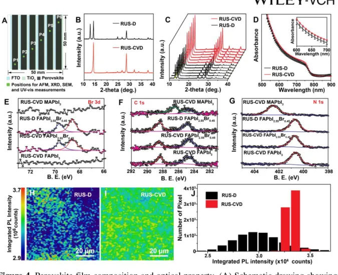
8
FAPb(IxBr1-x)3 with x equal to 85% is employed as the target perovskite material owing to its 1
superior thermal stability as reported by previous studies.57-59 For the films prepared by the 2
RUS-D method, the Br- to (I- + Br-) molar ratio is around 15% according to their ratio in the 3
dipping solution. To make the two conversion methods comparable, we optimize the RUS-CVD 4
process so as to prepare the perovskite with the similar composition. XRD and UV-Vis 5
measurements are performed on 6 different locations of each 5 cm × 5 cm substrate to study the 6
composition of the perovskite films (Figure 4A). Perovskite films converted by RUS-CVD and 7
RUS-D show very similar XRD peak positions at 14.1˚, 24.5˚, 28.3˚, 31.8˚, 33.7˚, assigned to 8
(-111), (021), (222), (231), (030) perovskite crystal planes, respectively, suggesting that the 9
perovskite films are of a similar composition (Figure 4B). Peak positions agree well with those 10
of FAPb(I0.85Br0.15)3.58 The peaks at 26.4˚, 37.7˚ belong to the FTO substrate. RUS-CVD 11
processed perovskite film shows much higher intensity of the (-111), (222) and (231) diffraction 12
peaks but lower XRD intensity at (021) than the RUS-D processed perovskite film. These 13
results suggest that the perovskite films prepared by different methods show different 14
crystalline alignment and RUS-CVD processed perovskite film shows a higher overall degree 15
of crystallinity. Moreover, perovskite films prepared by RUS-D show clear PbI2 peaks (12.7˚, 16
38.6˚), similar to our previous study.34 XRD patterns on the same sample but different positions 17
are similar, suggesting the data are representative for large area (Figure 4C). To quantify the 18
PbI2 crystalline phase fraction in the films, we perform the Rietveld refinement based on the 19
XRD results. A negligible PbI2 phase fraction is determined for the films prepared by RUS- 20
CVD, while 10±1% (wt) PbI2 is determined for the films prepared by RUS-D (Table S1).
21
Although a small amount of PbI2 existing at the perovskite grain boundary is reported to be 22
beneficial for the defect passivation,60 such a large amount of PbI2 is expected to be detrimental 23
to the solar cell performance, due to the absorbance loss. To verify this point, we conduct UV- 24
Vis spectroscopy measurements on these films. Indeed, absorbance is lower for the films 25
prepared by RUS-D (Figure 4D). Furthermore, variation of the absorbance at same sample but 26
9
different positions is 6-8 times smaller for the RUS-CVD method at wavelength between 600 1
– 700 nm, suggesting the RUS-CVD prepared perovskite film is more uniform at the 2
macroscopic scale (detection area is 0.3 cm × 0.5 cm for each measurement) (Figure 4D inset).
3
Absorbance edges for the two perovskite films are both at ~790 nm, agreeing well with that for 4
the FAPb(I0.85Br0.15)3 perovskite.58 5
Effect of MACl during the perovskite formation.
6
MACl is added for both dipping and CVD conversion processes. In the dipping process, MACl 7
strongly affects the perovskite crystallization process and leaves the films after thermal 8
annealing.61 We find that creation of MACl atmosphere during the perovskite formation via the 9
CVD process also influences the perovskite crystallization, resulting in increase of the 10
perovskite (-111) and (222) peak intensity (Figure S5A and S5B) and reduced perovskite film 11
surface roughness (Figure S5C and S5D). Perovskite converted via CVD with or without MACl 12
atmosphere shows negligible change in the XRD peak position, suggesting that the Cl- amount 13
incorporated into the perovskite lattice is not significant (Figure S5B).62 To study whether FA+ 14
is partially substituted by the MA+ cation, we conduct high resolution X-ray photoelectron 15
spectroscopy (HRXPS) measurements on the two FAPb(I0.85Br0.15)3 perovskite prepared by 16
RUS-CVD and RUS-D and also on the RUS-CVD prepared MAPbI3 and FAPbI3 perovskite as 17
control. Little peak position change appears for the Pb 4f and I 3d regions comparing the four 18
samples (Figure S6A and S6B). Br 3d signals appear in the two FAPb(I0.85Br0.15)3 perovskite 19
films (Figure 4E). Two peaks at 288.5 and 284.8 eV assigned to FA+ related C 1s peaks appear 20
for the two FAPb(I0.85Br0.15)3 perovskite films and no typical MA+ peak (286.5 eV) appears, 21
indicating that no or only a very small amount of MA+ substitutes the FA+ position (Figure 22
4F).19, 44 The statement is further confirmed by the N 1s peak position. The two 23
FAPb(I0.85Br0.15)3 perovskite films show the N 1s peak at 400.7 eV similar to FAPbI3, where 24
the N 1s peak associated with MA+ appears at 402.5 eV (Figure 4G).19, 44 PL mapping is a 25
spatially resolved technique that can characterize uniformity and quality of the photoactive 26
10
layer. We carry out the PL mapping measurements on 4 different positions of each perovskite 1
film (detection area is 80 μm × 80 μm) and quantitatively compare the PL emission results. The 2
CVD-converted perovskite films show not only a ~10% higher PL intensity, but also ~5 times 3
narrower PL intensity distribution than dipping-converted perovskite (Figure 4H, 4I, 4J, Figure 4
S7A-H). Based on the results, we conclude that perovskite films prepared by RUS-CVD 5
method reveal higher uniformity across large area and higher quality than RUS-D from the 6
purity, crystallinity and optical property point of view.
7
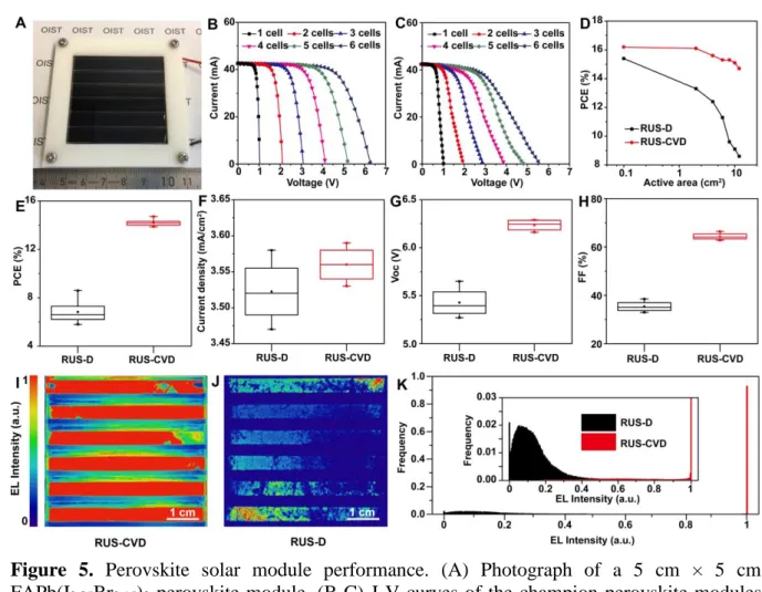
Perovskite solar cell/module performance and reproducibility.
8
To study the device performance, we prepare perovskite modules by RUS-CVD and RUS-D on 9
5 cm × 5 cm substrates, where each contains 6 cells connected in series with a total active area 10
of 12.0 cm2 (Figure 5A). A patterned TiO2 layer was deposited by a scalable vacuum sputtering 11
method as the elerctron transporting layer.63-64 No mesoporous TiO2 layer is used because of 12
the patterning difficulty. We are not aiming at demonstrating deposition methods for the 13
complete perovskite solar module. Therefore the deposition process for other layers (e.g., hole 14
transport layer) may not be scalable. The modules are patterned by 3 shadow masks. Details of 15
the module geometry are shown in Figure S8 and discussed in the supporting information.44 J- 16
V measurements are conducted on the modules with 1 to 6 cells connected in series to determine 17
the performance on different device active area. The champion module prepared by the RUS- 18
CVD shows a Voc of 6.29 V, Isc of 42.6 mA, FF of 66.5%, and PCE of 14.7% for the 6 sub-cells 19
connected in series from forward to backward scan (Figure 5B) and a PCE of 13.5% from 20
backward to forward scan (Figure S9A). As far as we know, this is among the highest 21
performing perovskite solar module prepared by spray-coating method to date.34, 42, 65 In 22
addition, performance of the champion RUS-CVD modules slowly decreases from 16.1% on 2 23
cm2 to 14.7% on 12 cm2 (Figure 5D and Table S2), corresponding to a very low PCE loss/area 24
(defined as (PCEsingle cell − PCEmodule)/(areamodule − areasingle cell)) of 0.14 %/cm2.44 On the other 25
hand, the champion module prepared by RUS-D shows a much lower PCE of 8.6% from 26
11
forward to backward scan and a PCE of 6.8% from backward to forward scan (Figure 5C and 1
Figure S9B). Performance of the champion RUS-D modules decreases much faster from 13.3%
2
on 2 cm2 to 8.6% on 12 cm2 (Figure 5D and Table S2), corresponding to a high PCE loss/area 3
(defined as (PCEsingle cell − PCEmodule)/(areamodule − areasingle cell)) of 0.47 %/cm2. Such a big PCE 4
loss/area gap between the two perovskite processing methods indicates that the RUS-CVD 5
perovskite shows higher uniformity and lower series resistance at the perovskite absorber and 6
related interfaces (see Supplementary Information for details of the reasons causing the module 7
performance decrease upon increase of the active area).
8
To study the reproducibility of the two perovskite fabrication approaches, 16 modules (8 9
modules prepared by RUS-CVD and 8 modules prepared by RUS-D) are prepared for statistical 10
analysis. Averaged PCEs are 14.2±0.3% (12 cm2 active area) for RUS-CVD prepared modules, 11
significantly higher than RUS-D prepared modules (6±1%) (Figure 5E). It is worth mentioning 12
that even for the modules prepared by RUS- D, the PCE has already exceeded that for the solar 13
module based on the perovskite film prepared by the combination of SUS-coated PbI2 and 14
dipping conversion (~8% champion module PCE on 10 cm2 active area).34 This result indicates 15
the advantage of the RUS process over our previously reported SUS process in PbI2 deposition 16
across large area. With perovskite film converted by CVD, the module performance is further 17
increased by 136.6% (PCE increase = (average PCERUS-CVD- average PCERUS-D) /average 18
PCERUS-D) than those converted by our reported dipping process. RUS-CVD prepared modules 19
shows only marginally higher average Jsc than RUS-D prepared modules, suggesting that Jsc is 20
not the main factor causing the performance variation. This is confirmed by external quantum 21
efficiency (EQE) measurements. The integrated currents are both 20.3 mA/cm2 for champion 22
modules prepared by RUS-D and RUS-CVD, agreeing well with the current values from J–V 23
measurement with variations of less than 5% (Figure S9C). Module performance differences 24
are mainly caused by differences in Voc and FF according to the statistical results (Figure 5F- 25
H), which can be related to the different perovskite film quality and uniformity.44 26
12 Perovskite solar module quality and uniformity.
1
To evaluate device quality and uniformity over the entire module area we performed spatially 2
resolved electroluminescence (EL) measurements.66 While PCE depends linearly on Voc, Isc, 3
and FF, EL intensity (LED efficiency) at a given current is exponentially dependent on quasi- 4
Fermi level separation (Voc).67 Exponential dependence on Voc leads to a much weaker 5
dependence on FF, and EL intensity probes the quality (non-radiative recombination rate) in 6
the absorber without sensitivity to resistive losses that would reduce measured FF in a PCE 7
measurement. Comparison of EL measurements between RUS-CVD and RUS-D modules 8
shows that RUS-D modules have a lower EL intensity in most locations whereas RUS-CVD 9
modules have dramatically higher EL intensity at the same applied current (Figure 5I and 5J).
10
We plot the EL intensity histogram figure to evaluate the EL intensity as a function of frequency.
11
RUS-D module shows a wide EL intensity distribution between 0-30% relative to the saturated 12
EL intensity, while RUS-CVD module shows over 90% distribution at the saturated EL 13
intensity (Figure 5K and 5K inset). Such dramatic differences in EL intensity suggest that the 14
RUS-CVD prepared perovskite has much less non-radiative recombination centers induced by 15
defects, which contributes to a higher module Voc and PCE.
16
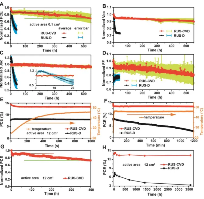
Perovskite solar cell/module operational stability.
17
Instability is one of the main challenges for perovskite solar cells. Because perovskite solar cell 18
lifetime varies substantially for different perovskite deposition methods, it is necessary to report 19
the device lifetime for newly developed methods. Conditions for the device stability test such 20
as atmosphere, temperature, illumination (continuous light soaking or storage under dark) and 21
load applied (open circuit, short circuit or MPP) significantly affect the device lifetime.68 22
Device stability evaluation based on statistical results is also recommended.69 Considering these 23
reasons, we prepare 8 FAPb(I0.85Br0.15)3 perovskite solar cells (0.1 cm2 active area) in two 24
different batches (4 cells prepared by RUS-CVD and 4 cells prepared by RUS-D) and conduct 25
the first operational stability measurements on these devices. The devices are kept at continuous 26
13
1 sun illumination near their MPP, in the N2 atmosphere (<5% relative humidity), without 1
encapsulation at room temperature (25.0 ˚C) and measured by step J-V scans every 30 min 2
(Figure S10A and S10B). Similar to other reports, RUS-CVD prepared devices show the initial 3
transient PCE decay (i.e., the exponential regime), which is followed by the linearly decay (i.e., 4
the linear regime) (Figure 6A).68 Transient decay is generally recoverable if the device is stored 5
in dark for an extended time.68 Therefore the T80 parameter, which represents the time when 6
PCE decays to 80%, can be calculated based on the linear decay regime.68 RUS-CVD prepared 7
devices show an average T80 value of 535 h (Figure 6A brown line to green line), closing to the 8
highest reported lifetime for planar structured perovskite solar cells.13 Such a high T80 lifetime 9
suggests that RSU-CVD prepared devices are very stable under the operational condition. In a 10
previous study, we report the poor device stability for the CVD converted FAPbI3 perovskite 11
solar modules due to formation of the yellow non-perovskite phase.44 Here we demonstrate that 12
by adding 15% Br in the perovskite, stability of the perovskite solar cells is significantly 13
improved. We find all of the Jsc, Voc and FF decay with time and the majority of PCE decay 14
comes from the FF (Figure 6B-D). In comparison, RUS-D prepared devices decay linearly at a 15
much higher rate, corresponding to an average T80 value of 8 h (Figure 6A). Different from 16
RUS-CVD prepared device, Jsc of RUS-D prepared devices increase by 20% until reaching the 17
maximum value and then decrease constantly (Figure 6C inset). The majority factor casing the 18
PCE decay is Jsc, not the FF (Figure 6B-D). The nearly 70 times larger T80 value for the RUS- 19
CVD prepared device than the RUS-D case suggests the excellent long-term stability of the 20
cells based on our RUS-CVD method.
21
So far, most of the operational stability tests are conducted on small-sized solar cells (e.g., 22
active area ~ 0.1 cm2), not large-sized perovskite solar modules. The non-uniformity issue of 23
the perovskite film is more pronounced on the enlarged substrate, which has more changes to 24
cause the device failure under operation. On the other hand, temperature of the module increases 25
greatly under continuous illumination, which may also affect their performance and lifetime.45 26
14
Thus, it is important to study the operational stability of the perovskite modules at elevated 1
temperature. Here, we conduct the operation stability measurements at the similar condition as 2
for small cells on the FAPb(I0.85Br0.15)3 perovskite solar modules (active area 12 cm2). We 3
monitor the temperature during the operational stability measurements and find that the 4
temperature rapidly increases from 25.0 ˚C to > 46.0 ˚C during the first 1000 s (Figure 6E) and 5
stabilizes in the following period (Figure 6F). RUS-CVD prepared module follows the PCE 6
decay behavior of RUS-CVD prepared small cells, including an initial exponential decay 7
regime and a linear decay regime (Figure 6E and 6F). After 1200 min operation, the module 8
still shows a PCE of 13.3%, with only 0.2% PCE decay comparing to the module PCE after an 9
initial transient decay. This result suggests that the RUS-CVD prepared device is quite stable 10
at temperature of up to 46.0 ˚C. We measured the operation stability of another RUS-CVD 11
prepared perovskite module under the same condition until the device decayed to less than 80%
12
of its initial PCE. The RUS-CVD prepared device shows a long T80 lifetime of 388 h (Figure 13
6G brown line to green line). Comparing with the very few operational stability reports on the 14
perovskite solar modules46, 70, our RUS-CVD prepared module is very stable under such 15
measurement conditions. In comparison, RUS-D prepared perovskite module shows 65% PCE 16
decay from 8.1% to 2.8% after 1200 min operation. In addition, we also study the module 17
storage stability. One RUS-CVD prepared module and one RUS-D prepared module are stored 18
in dark N2 atmosphere (15% relative humidity) and measured in ambient air (~50% relative 19
humidity). After 3600 h, RUS-CVD prepared module still shows a PCE of 13.4%, with a 20
relative PCE decay of 3.6% (Figure 6H). In comparison, RUS-D prepared module shows a PCE 21
of 3.3% and a relative PCE decay of 47.4%. Based on all the stability results, we think the RUS- 22
CVD method is not only a scalable perovskite deposition method but also present promising 23
device stability on the solar module size.
24
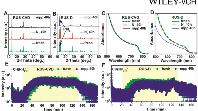
Perovskite decomposition and ion migration under operation condition 25
15
Furthermore, we study the reason causing the different device operational stability. Perovskite 1
solar cells fail under operation or storage for several reasons, such as light-, thermal- oxygen- 2
and humidity-induced perovskite degradation71-75, charge transporting layer decomposition76-77, 3
ion migration78-79 etc. Because the only difference in the two conditions comes from the 4
perovskite film, the perovskite degradation and ion migration can be considered as the main 5
factors that affect the device stability. We prepare perovskite solar cells by the two methods 6
and perform XRD and UV-vis measurements on these samples. Each method includes a fresh 7
device, the same device after 40 h storage in dark and N2 atmosphere and one operated device 8
under MPP condition for 40 h. Gold electrodes are removed before measurements. Devices 9
prepared by RUS-CVD show negligible change in XRD pattern after storage in dark N2
10
atmosphere or operation (Figure 7A). On the other hand, the XRD peaks assigned to the 11
perovskite significantly decreased after 40 h operation for the RUS-D prepared devices (Figure 12
7B). The RUS-D prepared perovskite stored in dark N2 atmosphere does not decompose, 13
indicating that decomposition of perovskite is caused by the operation (light, bias). The 14
statement is further confirmed by the UV-vis absorbance spectroscopy results. There is little 15
change in the absorbance for the devices prepared by RUS-CVD (Figure 7C), but there has been 16
an obvious reduction in the absorbance between the wavelength of 500 and 790 nm, which can 17
be assigned to decomposition of perovskite material, for the operated device prepared by RUS- 18
D (Figure 7D). Instability of the perovskite material in turn affects the operation instability of 19
the device. Such a different perovskite material stability might be caused by the different 20
perovskite grain size (Figure 3E and 3F).80 To better understand the composition changes and 21
ion migration that relate to the device failure, we perform the second ion mass spectrometry 22
(SIMS) measurements on fresh and operated devices (40 h under MPP condition) prepared by 23
RUS-CVD and RUS-D. Operated devices are stored in the dark N2 atmosphere for 1-3 days 24
before the SIMS measurements, so the changes observed are irreversible ones.81 Signals of Au+, 25
Pb+, FA+, I+, Br+, Ti+, Sn+ appear sequentially in all of the 4 samples (Figure S11). We observe 26
16
no significant difference of the element distribution (FA+, Au+, Pb+, I+, Br+, Ti+, Sn+) between 1
fresh and operated devices that are prepared by RUS-CVD (Figure 7E and Figure S11).
2
However, we identify a redistribution and an intensity decrease of FA+ on RUS-D prepared 3
device after operation (Figure 7F). It has been reported that the FA+ redistribution can cause the 4
failure of the device after operation.81 Similar to the report, we do not see obvious I+ and Br+ 5
migration.81 The FA+ migration is likely to be another key factor causing the failure of the RUS- 6
D prepared device after operation at such a time scale. Taken together, the high operational 7
stability of RUS-CVD prepared devices could be explained by the robust perovskite film with 8
negligible decomposition and FA+ ion migration at such a time scale. These results confirm the 9
excellent stability of perovskite solar cells and modules based on our RUS-CVD method.
10
Comparing with the perovskite films processed by solution based methods when the perovskite 11
is usually formed by annealing for 20 min, the growth rate of CVD-processed perovskite is 12
much slower. The constant supply of organic halide vapors helps the perovskite recrystallize 13
through in situ annealing, leading to formation of high quality perovskite films.55 14
Conclusions 15
In summary, we develop a scalable perovskite deposition technology with combination of raster 16
ultrasonic spray coating and chemical vapor deposition. Our technology overcomes the coating 17
size limitation of the existing stationary spray and single-pass spray. Negligible lead waste 18
during the PbI2 deposition process makes this technology environmental friendly and 19
transferable to industry. FAPb(I0.85Br0.15)3 perovskite films prepared using this technology show 20
high quality and uniformity. Planar structured perovskite module fabricated basing on this 21
method shows a high module PCE of 14.7% on an active area of 12.0 cm2, closing to the highest 22
reported module performance with perovskite film deposited by ultrasonic spray-coating. The 23
device also shows high operational stability, corresponding to an average T80 lifetime of 535 h 24
on the small cells (0.1 cm2) and 388 h on the module (12 cm2).
25 26
17 Supporting Information
1
Supporting Information is available from the Wiley Online Library or from the author.
2 3
Acknowledgements 4
This work was supported by funding from the Energy Materials and Surface Sciences Unit of 5
the Okinawa Institute of Science and Technology Graduate University, the OIST R&D Cluster 6
Research Program, the OIST Proof of Concept (POC) Program, and JSPS KAKENHI Grant 7
Number JP18K05266.
8 9
Conflict of interest 10
The authors declare no conflict of interest.
11 12
References 13
[1] J. Burschka, N. Pellet, S. J. Moon, R. Humphry-Baker, P. Gao, M. K. Nazeeruddin, M.
14
Grätzel, Nature 2013, 499, 316-319.
15
[2] H. S. Kim, C. R. Lee, J. H. Im, K. B. Lee, T. Moehl, A. Marchioro, S. J. Moon, R.
16
Humphry-Baker, J. H. Yum, J. E. Moser, M. Grätzel, N. G. Park, Sci. Rep. 2012, 2, 591.
17
[3] M. Liu, M. B. Johnston, H. J. Snaith, Nature 2013, 501, 395-398.
18
[4] National Renewable Energy Laboratory (NREL).
19
http://www.nrel.gov/ncpv/images/efficiency_chart.jpg (accessed Febrary, 2018).
20
[5] W. Ke, C. C. Stoumpos, M. Zhu, L. Mao, I. Spanopoulos, J. Liu, O. Y. Kontsevoi, M.
21
Chen, D. Sarma, Y. Zhang, M. R. Wasielewski, M. G. Kanatzidis, Sci. Adv. 2017, 3, e1701293.
22
[6] F. Jiang, D. Yang, Y. Jiang, T. Liu, X. Zhao, Y. Ming, B. Luo, F. Qin, J. Fan, H. Han, 23
L. Zhang, Y. Zhou, J Am. Chem. Soc. 2018, 140, 1019-1027.
24
[7] W. Ke, C. C. Stoumpos, I. Spanopoulos, L. Mao, M. Chen, M. R. Wasielewski, M. G.
25
Kanatzidis, J. Am. Chem. Soc. 2017, 139, 14800-14806.
26
[8] Y. Liao, H. Liu, W. Zhou, D. Yang, Y. Shang, Z. Shi, B. Li, X. Jiang, L. Zhang, L. N.
27
Quan, R. Quintero-Bermudez, B. R. Sutherland, Q. Mi, E. H. Sargent, Z. Ning, J. Am. Chem.
28
Soc. 2017, 139, 6693-6699.
29
18
[9] R. Nie, A. Mehta, B. W. Park, H. W. Kwon, J. Im, S. I. Seok, J. Am. Chem. Soc. 2018, 1
140, 872-875.
2
[10] S. Shao, J. Liu, G. Portale, H.-H. Fang, G. R. Blake, G. H. ten Brink, L. J. A. Koster, M.
3
A. Loi, Adv. Energy Mater. 2018, 8, 1702019.
4
[11] A. H. Slavney, T. Hu, A. M. Lindenberg, H. I. Karunadasa, J. Am. Chem. Soc. 2016, 5
138, 2138-2141.
6
[12] X. G. Zhao, J. H. Yang, Y. Fu, D. Yang, Q. Xu, L. Yu, S. H. Wei, L. Zhang, J. Am.
7
Chem. Soc. 2017, 139, 2630-2638.
8
[13] H. Tan, A. Jain, O. Voznyy, X. Lan, F. P. G. D. Arquer, J. Z. Fan, R. Quintero-Bermudez, 9
M. Yuan, B. Zhang, Y. Zhao, F. Fan, P. Li, L. N. Quan, Y. Zhao, Z.-H. Lu, Z. Yang, S.
10
Hoogland, E. H. Sargent, Science 2017, 355, 722-726.
11
[14] S. S. Shin, E. J. Yeom, W. S. Yang, S. Hur, M. G. Kim, J. Im, J. Seo, J. H. Noh, S. I.
12
Seok, Science 2017, 356, 167-171.
13
[15] K. A. Bush, A. F. Palmstrom, Z. J. Yu, M. Boccard, R. Cheacharoen, J. P. Mailoa, D. P.
14
McMeekin, R. L. Z. Hoye, C. D. Bailie, T. Leijtens, I. M. Peters, M. C. Minichetti, N. Rolston, 15
R. Prasanna, S. Sofia, D. Harwood, W. Ma, F. Moghadam, H. J. Snaith, T. Buonassisi, Z. C.
16
Holman, S. F. Bent, M. D. McGehee, Nat. Energy 2017, 2, 17009.
17
[16] L. Qiu, L. K. Ono, Y. Jiang, M. R. Leyden, S. R. Raga, S. Wang, Y. B. Qi, J. Phys.
18
Chem. B 2018, 122, 511-520.
19
[17] F. Bella, G. Griffini, J.-P. Correa-Baena, G. Saracco, M. Grätzel, A. Hagfeldt, S. Turri, 20
C. Gerbaldi, Science 2016, 354, 203-206.
21
[18] M. Saliba, T. Matsui, K. Domanski, J.-Y. Seo, A. Ummadisingu, S. M. Zakeeruddin, J.- 22
P. Correa-Baena, W. R. Tress, A. Abate, A. Hagfeldt, M. Grätzel, Science 2016, 354, 206-209.
23
[19] Y. Jiang, E. J. Juarez-Perez, Q. Ge, S. Wang, M. R. Leyden, L. K. Ono, S. R. Raga, J.
24
Hu, Y. B. Qi, Mater. Horiz. 2016, 3, 548-555.
25
19
[20] W. Chen, Y. Wu, Y. Yue, J. iu, W. Zhang, X. Yang, H. Chen, E. Bi, I. Ashraful, M.
1
Grätzel, L. Han, Science 2015, 350, 944-948.
2
[21] S. R. Raga, Y. Jiang, L. K. Ono, Y. B. Qi, Energy Technol. 2017, 5, 1750-1761.
3
[22] M. Cai, Y. Wu, H. Chen, X. Yang, Y. Qiang, L. Han, Adv. Sci. 2017, 4, 1600269.
4
[23] Z. Song, C. L. McElvany, A. B. Phillips, I. Celik, P. W. Krantz, S. C. Watthage, G. K.
5
Liyanage, D. Apul, M. J. Heben, Energy Environ. Sci. 2017, 10, 1297-1305.
6
[24] N. L. Chang, A. W. Y. Ho-Baillie, P. A. Basore, T. L. Young, P. Evans, Prog. Photovolt:
7
Res. Appl. 2017, 25, 390-405.
8
[25] N. L. Chang, A. W. Y. Ho-Baillie, D. Vak, M. Gao, M. A. Green, R. J. Egan, Sol. Energy 9
Mater. Sol. Cells 2018, 174, 314-324.
10
[26] M. Yang, Z. Li, M. O. Reese, O. G. Reid, D. H. Kim, S. Siol, T. R. Klein, Y. Yan, J. J.
11
Berry, M. F. A. M. van Hest, K. Zhu, Nat. Energy 2017, 2, 17038.
12
[27] Z. Li, T. R. Klein, D. H. Kim, M. Yang, J. J. Berry, M. F. A. M. van Hest, K. Zhu, Nat.
13
Rev. Mater. 2018, 3, 18017.
14
[28] J. J. Berry, J. van de Lagemaat, M. M. Al-Jassim, S. Kurtz, Y. Yan, K. Zhu, ACS Energy 15
Lett. 2017, 2, 2540-2544.
16
[29] M. Remeika, Y. B. Qi, J. Energy Chem. 2017, 27, 1101-1110.
17
[30] Y. Deng, Q. Wang, Y. Yuan, J. Huang, Mater. Horiz. 2015, 2, 578-583.
18
[31] M. Yang, D. H. Kim, T. R. Klein, Z. Li, M. O. Reese, B. J. Tremolet de Villers, J. J.
19
Berry, M. F. A. M. van Hest, K. Zhu, ACS Energy Lett., 2018, 3, 322-328.
20
[32] G. Cotella, J. Baker, D. Worsley, F. De Rossi, C. Pleydell-Pearce, M. Carnie, T. Watson, 21
Sol. Energy Mater. Sol. Cells 2017, 159, 362-369.
22
[33] S. Das, B. Yang, G. Gu, P. C. Joshi, I. N. Ivanov, C. M. Rouleau, T. Aytug, D. B.
23
Geohegan, K. Xiao, ACS Photonics 2015, 2, 680-686.
24
[34] M. Remeika, S. R. Raga, S. Zhang, Y. B. Qi, J. Mater. Chem. A 2017, 5, 5709-5718.
25
20
[35] S. Uličná, B. Dou, D. H. Kim, K. Zhu, J. M. Walls, J. W. Bowers, M. F. A. M. van Hest, 1
ACS Appl. Energy Mater. 2018, 1, 1853-1857.
2
[36] A. T. Barrows, A. J. Pearson, C. K. Kwak, A. D. F. Dunbar, A. R. Buckley, D. G. Lidzey, 3
Energy Environ. Sci. 2014, 7, 2944-2950.
4
[37] J. G. Tait, S. Manghooli, W. Qiu, L. Rakocevic, L. Kootstra, M. Jaysankar, C. A. Masse 5
de la Huerta, U. W. Paetzold, R. Gehlhaar, D. Cheyns, P. Heremans, J. Poortmans, J. Mater.
6
Chem. A 2016, 4, 3792-3797.
7
[38] H. Huang, J. Shi, L. Zhu, D. Li, Y. Luo, Q. Meng, Nano Energy 2016, 27, 352-358.
8
[39] F. Hilt, M. Q. Hovish, N. Rolston, K. Brüning, C. J. Tassone, R. H. Dauskardt, Energy 9
Environ. Sci. 2018, 11, 2102-2113.
10
[40] J. H. Heo, M. H. Lee, M. H. Jang, S. H. Im, J. Mater. Chem. A 2016, 4, 17636-17642.
11
[41] J. E. Bishop, J. A. Smith, C. Greenland, V. Kumar, N. Vaenas, O. S. Game, T. J.
12
Routledge, M. Wong-Stringer, C. Rodenburg, D. G. Lidzey, ACS Appl. Mater. Interfaces 2018, 13
10, 39428-39434.
14
[42] S.-G. Li, K.-J. Jiang, M.-J. Su, X.-P. Cui, J.-H. Huang, Q.-Q. Zhang, X.-Q. Zhou, L.-M.
15
Yang, Y.-L. Song, J. Mater. Chem. A 2015, 3, 9092-9097.
16
[43] K. Cao, Z. Zuo, J. Cui, Y. Shen, T. Moehl, S. M. Zakeeruddin, M. Grätzel, M. Wang, 17
Nano Energy 2015, 17, 171-179.
18
[44] Y. Jiang, M. R. Leyden, L. Qiu, S. Wang, L. K. Ono, Z. Wu, E. J. Juarez-Perez, Y. B.
19
Qi, Adv. Funct. Mater. 2018, 28, 1703835.
20
[45] M. R. Leyden, Y. Jiang, Y. B. Qi, J. Mater. Chem. A 2016, 4, 13125-13132.
21
[46] H. Chen, F. Ye, W. Tang, J. He, M. Yin, Y. Wang, F. Xie, E. Bi, X. Yang, M. Grätzel, 22
L. Han, Nature 2017, 550, 92-95.
23
[47] Wikipedia. https://en.wikipedia.org/wiki/Chemical_vapor_deposition (accessed 24
December, 2018).
25
21
[48] Poly plant project. https://www.polyplantproject.com/cvdreactors.html (accessed 1
December, 2018) 2
[49] Kaneka Corporation. http://www.kaneka-solar.com/product/thin-film/pdf/U-EA.pdf 3
(accessed December, 2018).
4
[50] Sono-Tek Corporation. http://www.sono-tek.com/thin-film-overview/ (accessed 5
Febrary, 2018).
6
[51] N. Ahn, D. Y. Son, I. H. Jang, S. M. Kang, M. Choi, N. G. Park, J. Am. Chem. Soc.
7
2015, 137, 8696-8699.
8
[52] Y. Wu, A. Islam, X. Yang, C. Qin, J. Liu, K. Zhang, W. Peng, L. Han, Energy Environ.
9
Sci. 2014, 7, 2934-2938.
10
[53] Wikipedia. https://en.wikipedia.org/wiki/Dimethylformamide (accessed December, 11
2018).
12
[54] Wikipedia. https://en.wikipedia.org/wiki/Dimethyl_sulfoxide (accessed December, 13
2018).
14
[55] J. Yin, H. Qu, J. Cao, H. Tai, J. Li, N. Zheng, J. Mater. Chem. A 2016, 4, 13203-13210.
15
[56] W. Qiu, T. Merckx, M. Jaysankar, C. M. Huerta, L. Rakocevic, W. Zhang, U. W.
16
Paetzold, R. Gehlhaar, L. Froyen, J. Poortmans, D. Cheyns, H. J. Snaith, P. Heremans, Energy 17
Environ. Sci., 2016, 9, 484-489.
18
[57] Q. Jiang, L. Zhang, H. Wang, X. Yang, J. Meng, H. Liu, Z. Yin, J. Wu, X. Zhang, J.
19
You, Nat. Energy 2016, 2, 16177.
20
[58] G. E. Eperon, S. D. Stranks, C. Menelaou, M. B. Johnston, L. M. Herz, H. J. Snaith, 21
Energy Environ. Sci. 2014, 7, 982.
22
[59] J. W. Lee, D. J. Seol, A. N. Cho, N. G,Park, Adv. Mater. 2014, 26, 4991-4998.
23
[60] Q. Chen, H. Zhou, T. B. Song, S. Luo, Z. Hong, H. S. Duan, L. Dou, Y. Liu, Y. Yang, 24
Nano Lett. 2014, 14, 4158-4163.
25
[61] Y. Zhao, K. Zhu, J. Phys. Chem. C 2014, 118, 9412-9418.
26
22
[62] C. Mu, J. Pan, S. Feng, Q. Li, D. Xu, Adv. Energy Mater. 2017, 7, 1601297.
1
[63] Wikipedia. https://en.wikipedia.org/wiki/Sputter_deposition (accessed December, 2
2018).
3
[64] Kaivo Optoelectronic Technology Co. Ltd. http://www.zh- 4
kv.com/Kaivo_En/ProductView.asp?ID=19&SortID=128 (accessed December, 2018).
5
[65] J. E. Bishop, T. J. Routledge, D. G. Lidzey, J. Phys. Chem. Lett. 2018, 9, 1977-1984.
6
[66] D. Abou-Ras, Rau, U. Thomas Kirchartz, Second edition. Weinheim: Wiley-VCH-Verl 7
2016.
8
[67] T. Kirchartz, U. Rau, M. Kurth, J. Mattheis, J. H. Werner, Thin Solid Films 2007, 515, 9
6238-6242.
10
[68] K. Domanski, E. A. Alharbi, A. Hagfeldt, M. Grätzel, W. Tress, Nat. Energy 2018, 3, 11
61-67.
12
[69] A. Tiihonen, K. Miettunen, J. Halme, S. Lepikko, A. Poskela, P. D. Lund, Energy 13
Environ. Sci. 2018, 11, 730-738.
14
[70] N. Yaghoobi Nia, M. Zendehdel, L. Cinà, F. Matteocci, A. Di Carlo, J. Mater. Chem. A 15
2018, 6, 659-671.
16
[71] A. Dualeh, P. Gao, S. I. Seok, M. K. Nazeeruddin, M. Grätzel, Chem. Mater. 2014, 26, 17
6160-6164.
18
[72] E. J. Juarez-Perez, Z. Hawash, S. R. Raga, L. K. Ono, Y. B. Qi, Energy Environ. Sci.
19
2016, 9, 3406-3410.
20
[73] E. J. Juarez-Perez, L. K. Ono, M. Maeda, Y. Jiang, Z. Hawash, Y. B. Qi, J. Mater. Chem.
21
A 2018, 6, 9604-9612.
22
[74] J. A. Christians, P. A. Miranda Herrera, P. V. Kamat, J. Am. Chem. Soc. 2015, 137, 23
1530-1508.
24
[75] N. Aristidou, C. Eames, I. Sanchez-Molina, X. Bu, J. Kosco, M. S. Islam, S. A. Haque, 25
Nat. Commun. 2017, 8, 15218.
26
23
[76] A. K. Jena, M. Ikegami, T. Miyasaka, ACS Energy Lett. 2017, 2, 1760-1761.
1
[77] Y. Zhao, W. Zhou, H. Tan, R. u, Q. Li, F. Lin, D. Yu, G. Walters, E. H. Sargent, Q.
2
Zhao, J. Phys. Chem. C 2017, 121, 14517-14523.
3
[78] Y. Yuan, J. Huang, Acc. Chem. Res. 2016, 49, 286-293.
4
[79] K. Domanski, J. P. Correa-Baena, N. Mine, M. K. Nazeeruddin, A. Abate, M. Saliba, 5
W. Tress, A. Hagfeldt, M. Grätzel, ACS Nano 2016, 10, 6306-6314.
6
[80] J. Ávila, C. Momblona, P. P. Boix, M. Sessolo, H. J. Bolink, Joule 2017, 1, 431-442.
7
[81] J. A. Christians, P. Schulz, J. S. Tinkham, T. H. Schloemer, S. P. Harvey, B. J. Tremolet 8
de Villers, A. Sellinger, J. J. Berry, J. M. Luther, Nat. Energy 2018, 3, 68-74.
9
24 1
2
Figure 1. Perovskite film deposition. (A) Schematic drawing of the RUS-CVD perovskite film 3
deposition technology. PbI2 films are raster ultrasonic spray (RUS)-coated on the FTO/ compact 4
TiO2 (c-TiO2) substrates, and converted to FAPbIxBr3-x via a CVD process. Photograph of (B) 5
a RUS-coated PbI2 film before annealing and (C) a CVD converted FAPbIxBr3-x film deposited 6
on a 10 cm × 10 cm patterned FTO substrate. (D) Solar cell and module performance as a 7
function of active area. Spin-coating data are extracted from our previous work.44 The RUS- 8
CVD method shows much lower substrate size dependence than the spin-coating method. (E) 9
Lead waste during the perovskite deposition process as a function of substrate size. Lead waste 10
during the RUS-CVD process continuously decreases until negligible, much less than that 11
generated during the spin-coating process.
12 13
25 1
Figure 2. Effect of solvent mixture on the PbI2 film texture. False-color monochrome scattered 2
light optical images of (A-D) PbI2 precursor films after spray-coating (solvent allowed to 3
evaporate at process temperature) (E-H) PbI2 precursor films after annealing to remove the 4
coordinated DMSO. Optical images show the entire 5 cm × 5 cm substrates. (I) Root mean 5
square (RMS) roughness of spray-coated PbI2 films. AFM measurements are performed on 6 6
positions of each 5 cm × 5 cm substrate for statistical analysis. The DMF : DMSO ratios are 7
14:0.5 for 2A, 2E; 14:0.65 for 2B, 2F; 14:0.85 for 2C, 2G and 14:1 for 2D, 2H, respectively.
8
(J-M) Schematic drawing showing the SLI mapping measurements on the different PbI2 films.
9
Increasing the DMSO ratio results in reduced film surface roughness but increased internal 10
cracks and voids.
11 12
26 1
Figure 3. Perovskite film morphology. (A-D) False-color monochrome scattered light optical 2
images of perovskite films. (E-H) AFM morphology of perovskite films. (I) Root mean square 3
(RMS) roughness of the FAPb(IxBr1-x)3 films. AFM measurements are performed on 6 positions 4
of each 5 cm × 5 cm substrate for statistical analysis. (J-M) Schematic drawing showing the 5
characteristics of the FAPb(IxBr1-x)3 films converted by CVD and the dipping (D) process. The 6
perovskite films are prepared by (A, E) RUS (DMF : DMSO = 14 : 0.65)-CVD, (B, F) RUS 7
(DMF : DMSO = 14 : 1)-CVD, (C, G) RUS (DMF : DMSO = 14 : 0.65)-D, (D, H) RUS (DMF : 8
DMSO = 14 : 1)-D, respectively. Perovskite films converted using RUS (DMF : DMSO = 14 : 9
0.65) PbI2 show high uniformity without pin-holes.
10 11
27 1
Figure 4. Perovskite film composition and optical property. (A) Schematic drawing showing 2
the 6 positions for the AFM, SEM, XRD, and UV-Vis measurements. (B-C) XRD pattern, (D) 3
UV-Vis absorbance spectra of FAPb(I0.85Br0.15)3 perovskite films. (E) Br 3d, (F) C 1s and (G) 4
N 1s HRXPS spectra on FAPb(I0.85Br0.15)3 perovskite films. (H-I) false-color monochrome PL 5
mapping images of the FAPb(I0.85Br0.15)3 films. (J) PL intensity histogram extracted from 6
Figure 4H-I. Perovskite films converted by CVD and dipping have the similar composition of 7
FAPb(I0.85Br0.15)3. The Perovskite films converted by CVD show complete conversion with 8
higher perovskite crystallinity, absorbance and PL intensity than the dipping converted 9
perovskite films.
10 11
28 1
Figure 5. Perovskite solar module performance. (A) Photograph of a 5 cm × 5 cm 2
FAPb(I0.85Br0.15)3 perovskite module. (B-C) J-V curves of the champion perovskite modules 3
prepared by (B) RUS-CVD and (C) RUS-D method. (D) Solar cell and module performance as 4
a function of active area. The RUS-CVD method shows higher module performance and lower 5
substrate-size dependence than the RUS-D method. Statistical results of the module (E) PCE, 6
(F) current density, (G) Voc and (H) fill factor. A total of 16 modules (8 modules prepared by 7
RUS-CVD and 8 modules prepared by RUS-D) are prepared for the statistical analysis. The 8
RUS-CVD prepared modules show higher performance than the RUS-D prepared modules 9
because of slightly higher Jsc and significantly higher Voc and FF. False-color monochrome 10
EL mapping images of perovskite modules prepared by (I) RUS-CVD and (J) RUS-D methods.
11
(K) EL intensity histogram extracted from Figure 5I-J. The inset is the histogram with low 12
maximum frequency in Y axis. The RUS-CVD prepared module shows higher EL intensity, 13
suggesting the RUS-CVD prepared perovskite has much less non-radiative recombination 14
centers.
15 16
29 1
Figure 6. Stability of the perovskite solar cells and module. (A) Normalized average efficiency, 2
(B) Voc, (C) Jsc and (D) FF obtained on 4 unencapsulated perovskite solar cells (active area = 3
0.1 cm2). Devices are kept at 1 sun, N2 atmosphere (<5% relative humidity), at their maximum 4
power point and measured by step J-V scans every 30 min. The inset of (C) is the enlarged 5
region of (C) between 0-20 h. Jsc of the RUS-D samples increases in the first 2 h until reach 6
the maximum value and then decreases. (E-F) Steady-state maximum power output (Vmpp of 7
4.50 V for RUS-CVD and 3.10 V for RUS-D) of the champion perovskite modules (active area 8
= 12 cm2). Measurements are performed at 1 Sun, MPP condition, N2 atmosphere, <5% relative 9
humidity and without encapsulation. (G) Normalized efficiency obtained on a RUS-CVD 10
prepared perovskite module under the MPP condition. (H) Storage stability of the perovskite 11
solar modules. Modules are stored in dark, N2 atmosphere. For the RUS-CVD sample (Figure 12
6A, 6G), the brown line indicates the starting point of the linear region and the green line shows 13
the time when PCE decays to 80% with respect to the starting point. The perovskite solar 14
cells/module prepared by RUS-CVD show higher operational and storage stability.
15 16
30 1
Figure 7. Effect of perovskite deposition methods on device operational stability. (A-B) XRD 2
patterns and (C-D) UV-vis absorbance spectra of fresh, storage and operated devices. Gold 3
electrodes are removed before measurements. Under the same operational condition (mpp 40 4
h), the RUS-CVD sample do not decompose but the RUS-D sample decomposes significantly.
5
(E-F) SIMS depth profile of FA+ upon degradation. Measurements are taken on the fresh and 6
operated devices that prepared by (E) RUS-CVD and (F) RUS-D. Under the same operational 7
condition (mpp 40 h), the RUS-CVD sample does not show FA+ ion migration but the RUS-D 8
sample shows obvious ion migration from the perovskite film surface to bulk. Different 9
perovskite film decomposition and FA+ ion migration behavior result in different device 10
operational stability.
11 12 13
31
A negligible-Pb-waste and upscalable perovskite film processing method combining raster 1
ultrasonic spray coating and chemical vapor deposition is developed. Planar-structured 2
perovskite solar module shows a PCE of 14.7% on an active area of 12 cm2, much lower 3
substrate-size dependence than the spin-coating method, and outstanding operational stability 4
near the maximum power point under 1 Sun light illumination (T80 lifetime of 388 h).
5 6
Keyword: perovskite, solar module, upscalable, Lead waste, stability 7
8 9
Yan Jiang, Mikas Remeika, Zhanhao Hu, Emilio J. Juarez-Perez, Longbin Qiu, Zonghao Liu, 10
Taehoon Kim, Luis K. Ono, Dae-Yong Son, Zafer Hawash, Matthew R. Leyden, Zhifang Wu, 11
Lingqiang Meng, Jinsong Hu, and Yabing Qi*
12 13
14
Negligible-Pb-Waste and Upscalable Perovskite Deposition Technology for High 15
Operational-Stability Perovskite Solar Modules 16
17
ToC figure 18
19
20 21