PAPER
Monolithically Integrated Wavelength-Routing Switch Using
Tunable Wavelength Converters with Double-Ring-Resonator
Tunable Lasers
Toru SEGAWA†a), Shinji MATSUO†, Takaaki KAKITSUKA†, Yasuo SHIBATA†, Members, Tomonari SATO†, Yoshihiro KAWAGUCHI†, Yasuhiro KONDO†, Nonmembers, and Ryo TAKAHASHI†, Member
SUMMARY We present an 8× 8 wavelength-routing switch (WRS) that monolithically integrates tunable wavelength converters (TWCs) and an 8× 8 arrayed-waveguide grating. The TWC consists of a double-ring-resonator tunable laser (DRR TL) allowing rapid and stable switching and a semiconductor-optical-amplifier-based optical gate. Two different types of dry-etched mirrors form the laser cavity of the DRR TL, which enable integration of the optical components of the WRS on a single chip. The monolithic WRS performed 1× 8 high-speed wavelength routing of a non-return-to-zero signal at 10 Gbit/s. The switching operation was demon-strated by simultaneously using two adjacent TWCs.
key words: monolithic integration, photonic integrated circuits, tunable laser, wavelength conversion, all-optical switch
1. Introduction
The rapid growth of optical communications networks due to the widespread use of the Internet and Internet-related services has led to a need for large-capacity and low-power-consumption nodes with varied traffic-engineering capabili-ties. Optical packet switching (OPS) is a potential solution that maximizes the throughput and flexibility of the network because of its packet-level granularity [1], [2]. However, im-plementation of an OPS network will require optical routers that surpass the performance of current electrical routers.
In current high-capacity electrical routers, an incoming packet is first segmented into a sequence of fixed-length and slow data cells at a line card. The cells are routed through a switch fabric consisting of multiple parallel switching planes and re-assembled into a packet at the line card [3]. This forwarding method is very complex and has become the major bottleneck in throughput, power consumption, la-tency, and size. A potential solution is a high-speed optical switch that can operate on a packet-by-packet basis without segmentation while maintaining data in the optical domain.
An optical switch in an optical router would ideally have low power consumption, small size, scalability, and data-format transparency, as well as a high-speed switch-ing capability. Although such an ideal optical switch has never been realized, a variety of optical switching technolo-gies have been proposed, including LiNbO3-, GaAs-, or
InP-Manuscript received August 23, 2010. Manuscript revised March 22, 2011.
†The authors are with NTT Photonics Laboratories, Atsugi-shi,
243-0198 Japan.
a) E-mail: [email protected] DOI: 10.1587/transele.E94.C.1439
based crosspoint switches with a multistage configuration [4], broadcast-and-select switches based on semiconductor-optical-amplifier (SOA) gate arrays [5], and wavelength-routing switches (WRSs) based on tunable wavelength con-verters (TWCs) followed by an arrayed-waveguide grating (AWG) [6]. Among these technologies, the WRS would have low power consumption and high scalability for larger throughput.
The TWC in WRSs consists of a high-speed tunable laser and an optical gate. Several types of tunable laser have been demonstrated, including sampled-grating/super-structure-grating distributed-Bragg-reflector (SG/SSG DBR) lasers [8], [9], modulated grating Y-branch (MGY) lasers [10], and grating coupler with rear sampled grating reflector (GCSR) lasers [11]. The tun-ing mechanism of these lasers is based on the free-carrier plasma effect produced by current injection, which changes the refractive index of the tuning sections within a few nanoseconds. However, the transient thermal effect which causes the wavelength of the tunable laser to drift remains a problem [12]. The wavelength drift has a much longer response time (millisecond order) compared with the mech-anism employed for fast tuning. In addition, the drift will cause loss and crosstalk in the WRS since the lasing wave-length can slip out of the pass-bands of the AWG filter fol-lowing the tunable laser. Therefore, fast and accurate tuning of the lasing wavelength is critical in order to switch each packet within a guard time of several nanoseconds. More-over, integrating the TWCs and the AWG monolithically on a single chip would be a promising way to reduce the power consumption, size, and cost of the WRS.
In this paper, we describe a monolithic WRS with a double-ring-resonator tunable laser (DRR TL). The DRR TL is characterized by low tuning current operation that en-ables rapid and stable tuning of the TWC [13]. An etched mirror was developed for the laser cavity of the DRR TL in the monolithic TWC. In addition, a highly reflective mirror coated with Au is used to improve the performance of the TWC.
This paper is organized as follows. Section 2 describes the operation principle and fabrication of the monolithic TWC with the DRR TL. Section 3 describes the monolithic WRS that integrates an array of eight TWCs and an 8× 8 AWG. Section 4 summarizes the main points.
2. Tunable Wavelength Converter with Double-Ring-Resonator Tunable Laser
2.1 Device Structure and Fabrication
A photograph of the fabricated TWC is shown in Fig. 1. The TWC consists of the DRR TL and an optical gate with a parallel amplifier structure (PAS) [14]. The DRR TL ex-hibited a tuning range of 50.0 nm with a current injection of less than 5.2 mA, providing rapid (less than 11 ns) and stable (less than 5 GHz wavelength drift) wavelength tun-ing [15]. Figure 1(b) shows a schematic of the DRR TL. The laser consists of a gain section, a phase control section, and a filter section. The filter section consists of two ring resonators that have slightly different free spectral ranges (FSRs). The wavelength tuning range of the filter section is greatly enhanced by the Vernier effect between the two ring resonators. Compared with the SG DBR often employed in tunable lasers, the ring-resonator filters employed within the cavity of the DRR TL have superior filter characteristics and a more compact structure. The characteristics include a nar-rower transmission bandwidth with a Lorentzian-type filter response and an infinite number of resonant peaks. When the Vernier tuning mechanism is used, the maximum injec-tion current required for tuning can be reduced by reducing FSRs of the filters. The ring-resonator filter can reduce the FSR while it expands the tuning range, resulting in low tun-ing current operation. The detailed operattun-ing principle of the DRR TL can be found in Ref. [15]. Low tuning current operation is critical for reducing the wavelength drift caused by thermal transients [15], and it is highly advantageous for high-speed and stable switching operation of the TWC.
The FSRs of the ring resonators were set to 400 (Ring 1) and 444 GHz (Ring 2), which correspond to ring radii of around 20μm. As a result, the total FSR of the two ring res-onators was 4 THz. Wavelength conversion is performed by modulating the CW light from the DRR TL with cross-gain modulation (XGM) caused by the input signal injected into
Fig. 1 (a) Photograph of the fabricated TWC. (b) Schematic of the DRR TL.
the optical gate. The optical gate with the PAS is a sym-metric Mach-Zehnder interferometer (MZI), which consists of two 3-dB multimode interference (MMI) couplers and an SOA in each arm. Since the MZI is set in the cross state by injecting the same amount of current into both SOAs, the input signal after the XGM and the converted signal are au-tomatically fed to different output ports of the MZI; Port 2 and Port 1, respectively [16]. Therefore, the input optical signal is removed before the AWG with the PAS (filter-free operation).
The device has a stacked-layer structure [17], which enables a single regrowth step. In this structure, a compres-sively strained multi-quantum well (MQW) layer for the ac-tive section is grown on top of a 0.3μm-thick InGaAsP layer (λg = 1.4 μm). The active layer and 1.4Q passive layer are
separated by a 10-nm-thick InP etch stop layer to allow for removal of the active layer in the passive section by selec-tive wet etching. A 1.5μm-thick p-InP cladding layer and a p-InGaAsP contact layer were grown over the entire surface after the wet etching process.
The gain sections of the DRR TL and the SOA sec-tions have a shallow-ridge waveguide structure, which was formed by selective wet etching with diluted HCl to stop at the top of the active layer. On the other hand, the ring resonators and the other section have a deep-ridge wave-guide structure. Figure 2(a) shows a scanning electron mi-crograph (SEM) image of the fabricated deep-ridge wave-guide. The deep-ridge waveguide has a very large refractive index difference in the lateral direction (refractive index of InGaAsP: 3.24, air: 1 or BCB: 1.54), which enables reduc-tion of the allowable bending radius and the device size due to the strong lateral optical confinement. The deep-ridge waveguide structure was formed by Cl2-based inductively
coupled plasma reactive ion etching (ICP-RIE) with only a
Fig. 2 SEM image of (a) the deep-ridge waveguide and (b) the etched front mirror.
lithography step. This simplifies the fabrication process of the TWC, since there is no need for any additional high-resolution lithography such as EB lithography or hologra-phy, which is required when fabricating DBR-type lasers. After both waveguide structures had been fabricated, the device was spin-coated with benzocyclobutene (BCB) for planarizing the substrate surface. Residual BCB on the sur-face was then removed by a following etching step. Elec-trodes were then formed by using a liftoff process. An anti-reflection (AR) film was formed on the input and output sides of the TWC. The input and output waveguides are an-gled to reduce the AR coating requirements. The lengths of the gain and SOA sections are 400 and 1300μm, respec-tively.
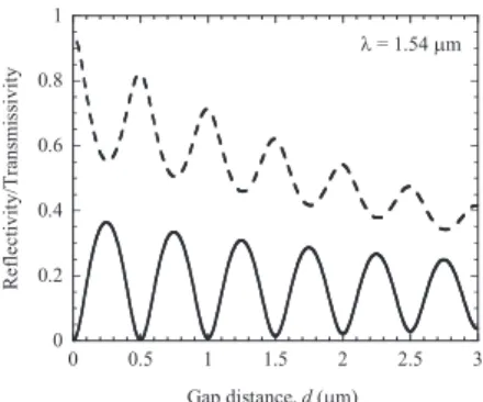
The laser cavity of the DRR TL is defined by the etched front and back mirrors [18]. Figure 2(b) shows an SEM image of the fabricated front etched mirror, which was lo-cated on the transition from the shallow-ridge to the deep-ridge waveguide structure. Figure 3 plots the reflectivity and transmissivity of the etched mirror at 1.54-μm wavelength, calculated as functions of the gap distance d by using the transfer matrix method. The calculation assumes the gap to be filled with BCB (refractive index: 1.54) and have a radiation loss of 1 dB/μm due to the diffraction in the gap. The radiation loss was estimated from a 3D-BPM simula-tion. As shown in the figure, the etched mirror has construc-tive and destrucconstruc-tive interferometric characteristics in rela-tion with d. Figure 4 shows calculated reflecrela-tion spectra of the etched mirror for different d. For d = 0.25 μm, the
mir-Fig. 3 Calculated reflectivity (solid line) and transmissivity (dashed line) of the etched gap mirror at a wavelength of 1.54μm.
Fig. 4 Calculated reflection spectra of the etched mirror.
ror is expected to have the largest reflectivity over a large bandwidth. However, it is difficult to fabricate a narrow and deep etched gap due to the micro-loading effect in ICP-RIE. For d= 0.75 μm, the mirror is expected to have a reflectivity of more than 30% over a 200-nm optical bandwidth. Since the fabrication error is considered to be less than±50 nm, a reflectivity of 30–34% should be achievable over a 50-nm optical bandwidth around the wavelength of 1.54μm. This reflectivity is enough for lasing over the wide tuning range, confirmed in calculations and an experiment. Therefore, d of 0.75μm was chosen for the device. Note that the etched mirror and deep-ridge waveguide were fabricated simulta-neously by ICP-RIE without any additional processes. 2.2 Wavelength Tuning and Wavelength Conversion
Char-acteristics
Figure 5 shows superimposed spectra of the fabricated TWC at Port 1 when the injection current of the gain and SOA sections were 120 and 100 mA, respectively. The device in this experiment was CW-operated at room temperature. The output light from the sample was coupled into a lensed fiber and detected with an optical spectrum analyzer. The thresh-old current and the maximum fiber-coupled output power were 40 mA and 3.6 dBm, respectively. When the injection current for both ring resonators was 0 mA, lasing was ob-served at 1542.1 nm. Next, the injection current of Ring 2 was increased from 0 to 7.7 mA, while that of Ring 1 was kept at 0 mA. The refractive index of the waveguide in Ring 2 decreased as the current increased, so that the reso-nant wavelength of Ring 2 gradually decreased. When the injection current was further increased to 5.4 mA, a corre-sponding increase in the lasing wavelength was observed up to 1561.4 nm. The lasing wavelength then jumped to 1536.0 nm at an injection current of 6.6 mA. The maximum injection currents are around one-fourth of those of an SG DBR laser designed for fast and accurate tuning [19]. The low-current operation with a wide tuning range can be at-tributed to the superior filter characteristics of the ring res-onator. The small injection currents needed for switching suppress the thermal wavelength drift of the laser [15].
Tunable wavelength conversion experiments were per-formed. Figure 6 shows the wavelength-converted eye
dia-Fig. 5 Superimposed lasing spectra of the fabricated TWC for various currents through the ring resonator with FSR of 444 GHz.
Fig. 6 Wavelength-converted eye diagrams of the fabricated TWC. (a) Changes in the eye diagram for different currents injected into both SOAs. (b) Changes in eye diagram for different wavelengths of the converted sig-nal.
grams of the fabricated TWC when a 10-Gbit/s non-return-to-zero (NRZ) input optical signal was fed into the input port. The PAS was set to the cross state by injecting the same amount of current into both SOAs. The input signal had a wavelength of 1550 nm with a pseudo-random bit se-quence (PRBS) of length 231 − 1. Figure 6(a) shows the
changes in the eye diagram in response to different SOA currents. The injection current of the gain section in the DRR TL was 125 mA. The wavelength of the converted sig-nal was tuned to 1541.7 nm by injecting current into Ring 2. As shown in Fig. 6(a), a higher SOA current results in faster conversion (shorter rise/fall time of the converted signal), since the conversion speed depends on the carrier-photon interaction in the SOAs. The speed can be increased by ei-ther increasing the injection current or the photon density in the SOAs. This has been studied extensively in Refs. [20] and [21]. Figure 6(b) shows the changes in the eye diagram for different wavelengths of the converted signal. The injec-tion currents of the gain and SOA secinjec-tions were kept con-stant at 125 and 250 mA, respectively. The wavelength of the converted signal was tuned from 1539.1 to 1558.0 nm. The extinction ratio decreased as the wavelength increased. The change in the extinction ratio with the wavelength of the converted signal is due to the variation in the differential gain with the signal wavelength [20]. When the wavelength of the CW light from the DRR TL is longer than that of the input signal, the CW light experiences a lower differential gain. Therefore, the conversion to a longer wavelength re-sults in a low extinction ratio.
Fig. 7 (a) Photograph of the fabricated WRS. (b) Enlarged view of the DRR TL.
3. Monolithically Integrated Wavelength-Routing Switch
3.1 Device Structure and Fabrication
Figure 7(a) shows a photograph of the fabricated WRS, con-sisting of an array of eight TWCs and an 8× 8 AWG. The device size is 2.1 mm × 4.8 mm, which is less than one-sixth the size of a previously reported 8× 8 monolithic optical switch [22]. Connections between the eight input and eight output ports are accomplished by changing the TWC output wavelength. Figure 7(b) shows an enlarged view of the DRR TL of the fabricated WRS. The FSRs of the ring resonators were set to 400 and 444 GHz, respectively. The total FSR of the two ring resonators is 4 THz, which sufficiently cov-ers the FSR of the AWG. The channel spacing of the 8× 8 AWG was set to 400 GHz, that is, equal to the FSR of one of the ring resonators. This enables a simple way to control a switching operation, since any output port can be selected by changing the injection current into the ring resonator with an FSR of 444 GHz.
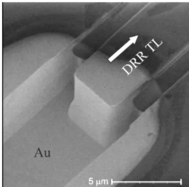
The laser cavity of the DRR TL is formed by the etched front mirror described in Sect. 2 and a highly reflective back mirror. For the TWC in Sect. 2, the etched mirror is used as both the front mirror and back mirror of the DRR TL. However, since an increase in the back reflectivity helps to improve the output power due to the reduction in the thresh-old current, the reflectivity of the back mirror of a DRR TL is required to be as high as possible. Therefore, a highly re-flective back mirror was developed to achieve a higher out-put power of the DRR TL and stabilize operation of the op-tical gate. Figure 8 shows an SEM image of the fabricated back mirror coated with Au. The back mirror was integrated with the DRR TL, in which a dry-etched facet was coated with Au. Figure 9 show the calculated reflectivity and trans-missivity of the mirror versus the thickness of the Au at a
Fig. 8 SEM image of highly reflective back mirror coated with Au.
Fig. 9 Calculated reflectivity (solid line) and transmissivity (dashed line) of the mirror at a wavelength of 1.55μm.
wavelength of 1.55μm. This calculation used a refractive index n of 0.559 and an extinction coefficient k of 9.81 [23]. The maximum reflectivity of the mirror should exceed 93% for around 100-nm-thick Au. The loss of around 7% in re-flection is considered to be caused by the absorption of Au. The dry-etched structure was fabricated in the same ICP-RIE step with the deep-ridge waveguide structure. The Au was deposited to a thickness of 300 nm by using a liftoff pcess employing electron-beam evaporation with angled ro-tation to improve sidewall coverage over the structure. AR film was formed on the input and output facets of the WRS. 3.2 Wavelength Routing Operation
The first results concern the static routing characteristics of the fabricated WRS. Figure 10 shows superimposed spectra of the WRS for every output port when using each TWC. The injection current for the ring resonator with an FSR of 444 GHz for each TWC changed from 0 to 8.9 mA, whereas the currents for the gain and both SOAs sections were kept constant at 100 and 200 mA, respectively. By changing the injection current for only a single ring resonator, the output ports can be easily selected, since the channel spacing of the AWG and the FSR of the other ring resonator were designed to be equal. The threshold current of a DRR TL with the highly reflective back mirror was 26 mA, which is 35% less than that of the DRR TL without the mirror in Sect. 2. The output power was−15 dBm of the previous WRS without the highly reflective back mirror [24], whereas the output
Fig. 10 Superimposed output spectra of the WRS for every output port using each TWC.
power of the current device is around 0 dBm. The small injection current needed for switching will suppress loss and crosstalk due to transient thermal effects in the monolithic WRS. The connection between each TWC output signal and WRS output through eight different wavelengths is based on the cyclic nature of the 8× 8 AWG.
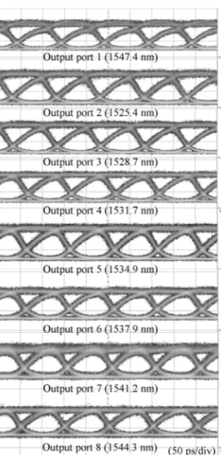
Figure 11 shows the wavelength-converted eye dia-grams for every output port of the WRS. In this experiment, only a single input port was tested. The 10-Gbit/s NRZ input
Fig. 11 Wavelength-converted eye diagrams for every output port of the WRS using the fifth TWC.
optical signal had a wavelength of 1545 nm with a PRBS of length 231− 1. The signal was fed into input port 5 with an
average power of 10 dBm. The wavelength of the converted signal was tuned so that the converted signal was output at one of eight output ports. The injection current for the ring resonator of the fifth TWC was varied from 0 to 6.6 mA, whereas the currents for the gain and both SOA sections were kept constant at 100 and 250 mA, respectively. A clear eye opening was observed for every output port, confirming the 1× 8 wavelength routing operation of the NRZ signal at 10 Gbit/s.
The next result is related to the high-speed wavelength routing operation of the WRS. Figure 12(a) shows signal waveforms from every output port of the WRS when the in-put signal was fed into inin-put port 5 (TWC5). The 10-Gbps NRZ input signal had a wavelength of 1545 nm with a power of 13 dBm. Dynamic switching among the eight output ports was performed by changing the injection current for only a single ring resonator with a period of 160 ns. High-speed, stable wavelength routing with a switching time of less than 10 ns was achieved (Fig. 12(b)). The switching time is sufficiently fast for the OPS application.
For the monolithic WRS, an important issue is ther-mal crosstalk between components, which leads to unsta-ble switching. Figure 13 shows signal waveforms from four output ports (output port 1, 3, 5 and 7) of the WRS when dynamic switching among the output ports was performed
Fig. 12 (a) Signal waveforms from all eight output ports of the WRS. (b) Expanded view at the switching from output port 4 to port 5.
Fig. 13 Signal waveforms from four output ports of the WRS.
by using two adjacent TWCs simultaneously. In this ex-periment, the currents for the gain and SOA sections were kept constant at 100 and 200 mA for TWC3 and at 120 and 200 mA for TWC4. The 10-Gbit/s NRZ input optical signal was fed into only TWC4 with an average power of 10 dBm. The injection current to one of the ring resonator of TWC4 was changed with a period of 320 ns. The output was
dy-namically switched among Port 1, 3, 5, and 7. Similarly, the current to a ring resonator of TWC3 was changed, but without inputting any signal. This indicates that the output comes just from the DRR TL. Fast, stable switching was achieved, even when the adjacent TWCs were simultane-ously employed. This can be attributed to the low tuning current operation of DRR TL, suppressing thermal crosstalk between the ring resonators.
4. Conclusion
We demonstrated an all-optical wavelength-routing switch with monolithically integrated TWCs and an 8×8 AWG. To monolithically integrate the DRR TL and optical gate based on PAS, we developed an etched mirror that can be imple-mented without any additional fabrication process. The pa-per described the opa-peration principle, fabrication, and char-acteristics of the monolithic TWC with the DRR TL. A highly reflective mirror coated with Au was developed to improve the performance of the TWC. We experimentally demonstrated 1× 8 high-speed wavelength routing of an NRZ signal at 10 Gbit/s with a switching time of less than 10 ns. The switching time between output ports is suffi-ciently fast for OPS. Simultaneous switching with adjacent TWCs was also demonstrated. The fast, stable switching ca-pability of the monolithic WRS can be attributed to the fast, stable, and low-power switching characteristics of the DRR TL.
Acknowledgments
This work was partially supported by the National Institute of Information and Communications Technology (NICT).
References
[1] S.J.B. Yoo, “Optical packet and burst switching technologies for the future photonic Internet,” J. Lightwave Technol., vol.24, no.12, pp.4468–4492, 2006.
[2] R. Takahashi, T. Nakahara, K. Takahata, H. Takenouchi, T. Yasui, N. Kondo, and H. Suzuki, “Ultrafast optoelectronic packet processing for asynchronous, optical-packet-switched networks,” OSA J. Opt. Netw., vol.3, pp.914–930, 2004.
[3] Cisco systems Inc, “Cisco carrier routing system,” http://www.cisco. com/en/US/prod/collateral/routers/ps5763/prod brochure0900aecd 800f8118.pdf
[4] M. Kohtoku, K. Kawano, S. Sekine, H. Takeuchi, N. Yoshimoto, M. Wada, T. Ito, M. Yanagibashi, S. Kondo, Y. Noguchi, and M. Naganuma, “High-speed InGaAlAs-InAlAs MQW directional cou-pler waveguide switch modules integrated with a spotsize converter having a lateral taper, thin-film core, and ridge,” J. Lightwave Tech-nol., vol.18, no.3, pp.360–369, 2000.
[5] P. Gambini, M. Renaud, C. Guillemot, F. Callegati, I. Andonovic, B. Bostica, D. Chiaroni, G. Corazza, S. Danielsen, P. Gravey, P.B. Hansen, M. Henry, C. Janz, A. Kloch, R. Krahenbuhl, C. Raffaelli, M. Schilling, A. Talneau, and L. Zucchelli, “Transparent opti-cal packet switching: Network architecture and demonstrators in the KEOPS project,” IEEE J. Sel. Areas Commun., vol.16, no.7, pp.1245–1259, 1998.
[6] J. Gripp, M. Duelk, J.E. Simsarian, A. Bhardwaj, P. Bernasconi, O.
Laznicka, and M. Zirngibl, “Optical switch fabrics for ultra-high-capacity IP routers,” J. Lightwave Technol., vol.21, no.11, pp.2839– 2849, 2003.
[7] K. Sasayama, et al., “FRONTIERNET: Frequency-routing-type time-division interconnection network,” J. Lightwave Technol., vol.15, no.3, pp.417–429, 1997.
[8] V. Jayaraman, Z.M. Chuang, and L. Coldren, “Theory, design, and performance of extended tuning range semiconductor lasers with sampled gratings,” IEEE J. Quantum Electron., vol.29, no.16, pp.1824–1834, 1993.
[9] H. Ishii, et al., “Multiple-phase-shift super structure grating DBR lasers for broad wavelength tuning,” IEEE Photonics Technol. Lett., vol.5, no.6, pp.613–615, 1993.
[10] J.-O. Wesstrom, et al., “Design of a widely tunable modulated grat-ing Y-branch laser usgrat-ing the additive Vernier effect for improved super-mode selection,” Proc. 18th IEEE Int. Semicond. Laser Conf. (ISLC 2002), TuP16, pp.99–100, 2002.
[11] M. Oberg, et al., “74 m wavelength tuning range of an InGaAsP/InP vertical grating assisted codirectional coupler laser with rear sam-pled grating reflector,” IEEE Photonics Technol. Lett., vol.5, no.8, pp.735–738, 1993.
[12] P. Kozodoy, T.A. Strand, Y.A. Akulova, G. Fish, C. Schow, P.-C. Koh, Z. Bian, J. Christofferson, and A. Shakouri, “Thermal effects in monolithically integrated tunable laser transmitters,” IEEE Trans. Compon. Packag. Manuf. Technol. A, vol.28, no.4, pp.651–657, 2005.
[13] T. Segawa, S. Matsuo, T. Kakitsuka, T. Sato, Y. Kondo, and H. Suzuki, “Full C-band tuning operation of semiconductor double ring resonator coupled laser with low tuning current,” IEEE Photonics Technol. Lett., vol.19, no.17, pp.1322–1324, 2007.
[14] Y. Shibata, N. Kikuchi, S. Oku, T. Ito, H. Okamoto, Y. Kawaguchi, Y. Suzuki, and Y. Kondo, “Monolithically integrated parallel-amplifier structure for filter-free wavelength conversion,” Jpn. J. Appl. Phys., vol.41, pp.1194–1198, 2002.
[15] T. Segawa, S. Matsuo, T. Kakitsuka, T. Sato, Y. Kondo, and R. Takahashi, “Semiconductor double-ring-resonator-coupled tunable laser for wavelength routing,” IEEE J. Quantum Electron., vol.45, no.7, pp.892–899, 2009.
[16] T. Segawa, S. Matsuo, T. Kakitsuka, Y. Shibata, T. Sato, Y. Kondo, and R. Takahashi, “Monolithically integrated filter-free wavelength converter with widely tunable double-ring resonator coupled laser,” Proc. 20th Indium Phosphide Related Mater. Conf. (IPRM 2008), TuA1.2, 2008.
[17] K. Sato, I. Kadota, K. Wakita, Y. Kondo, and M. Yamamoto, “Strained-InGaAsP MQW electroabsorption modulator integrated DFB laser,” Electron. Lett., vol.29, no.12, pp.1087–1088, 1993. [18] L. Coldren, K. Furuya, B. Miller, and J. Rentschler, “Etched
mir-ror and groove-coupled GaInAsP/InP laser devices for integrated optics,” IEEE J. Quantum Electron., vol.18, no.10, pp.1679–1688, 1982.
[19] J.E. Simsarian, M.C. Larson, H.E. Garrett, H. Xu, and T.A. Strand, “Less than 5-ns wavelength switching with an SG-DBR laser,” IEEE Photon. Technol. Lett., vol.18, no.4, pp.565–567, 2006.
[20] T. Durhuus, B. Mikkelsen, C. Joergensen, S.L. Danielsen, and K.E. Stubkjaer, “All-optical wavelength conversion by semiconductor op-tical amplifier,” J. Lightwave Technol., vol.14, no.6, pp.942–954, 1996.
[21] M. Asghari, I.H. White, and R.V. Penty, “Wavelength conversion using semiconductor optical amplifiers,” J. Lightwave Technol., vol.15, no.7, pp.1181–1190, 1997.
[22] S.C. Nicholes, M.L. Masanovic, B. Jevremovic, E. Lively, L.A. Coldren, and D.J. Blumenthal, “The world’s first InP 8× 8 mono-lithic tunable optical router (MOTOR) operating at 40 Gbps line rate per port,” Proc. Optical Fiber Comm. Conf. (OFC 2009), PDPB-1, 2009.
[23] E.D. Palik, Handbook of Optical Constants of Solids, Academic Press, 1985.
[24] T. Segawa, S. Matsuo, T. Kakitsuka, Y. Shibata, T. Sato, Y. Kawaguchi, Y. Kondo, and R. Takahashi, “Dynamic operation of a monolithic wavelength-routing switch using double-ring-resonator-coupled tunable laser diodes,” Proc. Int. Conf. Photonics in Switch-ing (PS 2009), WeI3-1, 2009.
Toru Segawa was born in Tokyo, Japan. He received the B.E. and M.E. degrees in electrical engineering from Keio University, Yokohama, Japan, in 1999 and 2001, respectively. In 2001, he joined NTT Photonics Laboratories, Atsugi, Japan and has been working on high-speed tun-able optical filters and lasers for optical packet switches. Mr. Segawa is a member of Japan So-ciety of Applied Physics (JSAP).
Shinji Matsuo received the B.S. and M.S. degrees in electrical engineering from Hiro-shima University, HiroHiro-shima, Japan, in 1986 and 1988, and the Ph.D. degree in electron-ics and applied physelectron-ics from Tokyo Institute of Technology, Tokyo, Japan, in 2008. In 1988, he joined NTT Opto-electronics Labora-tories, Atsugi, where he was engaged in research on photonic functional devices using MQW-pin modulators and VCSELs. In 1997, he re-searched optical networks using WDM tech-nologies at NTT Network Innovation Laboratories, Yokosuka. Since 2000, he has been researching high-speed tunable optical filters and lasers for photonic packet switching at NTT Photonics Laboratories, Atsugi. Dr. Matsuo is a member of the IEEE Lasers and Electro-Optics Society (LEOS) and Japan Society of Applied Physics.
Takaaki Kakitsuka was born in Kuma-moto, Japan, in 1971. He received the B.S. and M.S. degrees in physics from Kyushu Univer-sity, Fukuoka, Japan, in 1994 and 1996, respec-tively. In 1996, he joined NTT Opto-electronics Laboratories, Nippon Telegraph and Telephone Corporation (NTT), Kanagawa, Japan. He is engaged in research on semiconductor lasers and optical functional devices. He is now with NTT Photonics Laboratories. Mr. Kakitsuka is a member of the Japan Society of Applied Physics and the Physical Society of Japan.
Yasuo Shibata received the B.E. and M.E. degrees in electrical engineering, and Ph.D. de-gree in integrated design engineering from Keio University in 1985, 1987 and 2010, respectively. In 1987, he joined NTT Optoelectronics Labora-tories, Nippon Telegraph and Telephone Corpo-ration (NTT), Kanagawa, Japan, where he has been engaged in research on optical switches, optical filters and integrated devices. He is cur-rently with NTT Photonics Laboratories, en-gaged in research on modulators, tunable lasers, SOAs, and functional devices. Dr. Shibata is a member of the Japan Society of Applied Physics (JSAP) and IEEE/Photonics.
Tomonari Sato was born in Gunma, Japan, in 1978. He received the B.E., M.E., and D.E. degrees in engineering from University of Tsukuba, Ibaraki, Japan, in 2001, 2003, and 2009, respectively. In 2003, he joined NTT Pho-tonics Laboratories, Nippon Telegraph and Tele-phone Corporation (NTT), Kanagawa, Japan. He has been engaged in research on the MOVPE growth of III-V semiconductors and develop-ment of semiconductor lasers for sensor applica-tions. Dr. Sato is a member of the Japan Society of Applied Physics.
Yoshihiro Kawaguchi received B.S. and M.S. degrees in Applied Chemistry from Osaka University, Osaka, Japan, in 1981 and 1983, respectively. In 1983, he joined the Elec-trical Communication Laboratories, Nippon Telegraph and Telephone Corporation (present NTT), Kanagawa, Japan, where he had been en-gaged in research on MOMBE growth of III-V semiconductor. He is currently working on MOVPE growth of III-V materials for opto-electronics devices. He is a member of the Japan Society of Applied Physics.
Yasuhiro Kondo was born in Nagasaki, Japan, in 1961. He received the B.S. degree from Kumamoto University, Kumamoto, Japan, in 1984, and the M.S. degree in physics and the Ph.D. degree in electronic device engineer-ing from Kyushu University, Fukuoka, Japan, in 1986 and 1999, respectively. In 1986, he joined NTT Optoelectronics Laboratories, Kanagawa, Japan, where he has been engaged in research on MOVPE growth of III-V semiconductor and development of semiconductor lasers for trans-mission. He is now with NTT Photonics Laboratories. Dr. Kondo is a member of the IEEE Lasers and Electro-Optics Society (LEOS) and the Japan Society of Applied Physics.
Ryo Takahashi received the B.E., M.E., and D.E. degrees in electronic engineering from the University of Tokyo, Tokyo, Japan, in 1987, 1989, and 1992, respectively. In 1992, he joined NTT Opto-electronics Laboratories, Kanagawa, Japan. From 1998 to 1999, he was a Visit-ing Scholar at the Ginzton Laboratory, Stanford University, Stanford, CA. He is now with NTT Photonics Laboratories, Kanagawa, Japan, and has been engaged in R&D of ultrafast all-optical devices and optical packet processing technolo-gies for optical packet-switched networks. Dr. Takahashi is a member of the Japan Society of Applied Physics.