INVITED PAPER
Special Section on Electronic DisplaysTemperature Sensor employing Ring Oscillator composed of Poly-Si Thin-Film Transistors: Comparison between Lightly-Doped and O ff set Drain Structures
Jun TAYA†, Kazuki KOJIMA†, Tomonori MUKUDA†, Akihiro NAKASHIMA†, Yuki SAGAWA†, Tokiyoshi MATSUDA††,Nonmembers,andMutsumi KIMURA††a),Member
SUMMARY We propose a temperature sensor employing a ring os- cillator composed of poly-Si thin-film transistors (TFTs). Particularly in this research, we compare temperature sensors using TFTs with lightly- doped drain structure (LDD TFTs) and TFTs with offset drain structure (offset TFTs). First, temperature dependences of transistor characteristics are compared between the LDD and offset TFTs. It is confirmed that the offset TFTs have larger temperature dependence of the on current. Next, temperature dependences of oscillation frequencies are compared between ring oscillators using the LDD and offset TFTs. It is clarified that the ring oscillator using the offset TFTs is suitable to detect the temperature. We think that this kind of temperature sensor is available as a digital device.
key words: temperature sensor, ring oscillator, poly-Si, thin-film transistor (TFT), lightly-doped drain structure (LDD), offset drain structure
1. Introduction
Poly-Si thin-film transistors (TFTs) [1] have been widely applied to flat-panel displays (FPDs) [2], such as liquid- crystal displays (LCDs) [3] for not only computer moni- tors and mobile displays but also light valves in data projec- tors [4], organic light-emitting diode displays (OLEDs) [5], and electronic papers [6]. Because display properties of the liquid crystals [7], [8] and organic light-emitting diodes [9], [10] have temperature dependences, it is required to com- pensate them by controlling driving conditions. Actually, discrete temperature sensors are prepared near the LCDs for light valves, and the temperature dependences of the liquid crystals are compensated. However, because the tempera- tures have spatial distributions on the FPDs, it is required to measure the temperatures at several points and compensate the temperature dependences locally point by point.
Therefore, we proposed a temperature sensor employ- ing off-leakage currents of poly-Si TFTs to measure the temperatures at several points [11]–[13]. However, it was needed to equip analog voltage sensing circuits, which are fairly complicated circuits and difficult to be integrated on
Manuscript received January 7, 2014.
Manuscript revised April 30, 2014.
†The authors are with the Department of Electronics and Infor- matics, Ryukoku University, Otsu 520-2194, Japan.
†The authors are with the Department of Electronics and In- formatics, Ryukoku University, Otsu 520-2194, Japan, the Joint Research Center for Science and Technology, Ryukoku Univer- sity, Otsu 520-2194, Japan, and the High-Tech Research Center, Ryukoku University, Otsu 520-2194, Japan.
a) E-mail: [email protected] DOI: 10.1587/transele.E97.C.1068
the FPDs using poly-Si TFTs. Therefore, we proposed a temperature sensor employing a ring oscillator composed of poly-Si TFTs [14]. Although ring oscillators have been uti- lized to evaluate transistor characteristics [15]–[17], we be- lieve that this was the first report to apply a ring oscillator to a temperature sensor.
Incidentally, TFTs with lightly-doped drain structure (LDD TFTs) are indispensable to reduce off-leakage cur- rents and avoid characteristic degradation [18]–[24]. How- ever, TFTs with offset drain structure (offset TFTs) can be simultaneously fabricated without any additional fabrication process. Therefore, as for n-type TFTs, we are very inter- ested in which is suitable for a temperature sensor. On the other hand, as for p-type TFTs, because offset TFTs do not work at all, only LDD TFTs are used.
Again, we will propose a temperature sensor employ- ing a ring oscillator composed of poly-Si TFTs. Particularly in this research, we will compare temperature sensors using LDD and offset TFTs. First, temperature dependences of transistor characteristics will be compared between the LDD and offset TFTs. It will be confirmed which have larger tem- perature dependence of the on current. Next, temperature dependences of oscillation frequencies will be compared be- tween ring oscillators using the LDD and offset TFTs. It will be clarified which is suitable to detect the temperature.
2. LDD and Offset TFTs
First, the top-gate, coplanar, solid-phase crystallized (SPC), n-type and p-type, LDD and offset poly-Si TFTs are fab- ricated [25], [26]. Figure 1 shows the fabrication pro- cesses and device structures of the LDD and offset TFTs.
These fabrication processes are standard processes for mass production. An amorphous Si film is deposited on a quartz substrate using low-pressure chemical vapor depo- sition (LPCVD) of SiH4and crystallized using furnace an- nealing in N2ambient to form a poly-Si film. A SiO2 film is grown using thermal oxidation in O2 ambient and an- other SiO2film is stacked using chemical vapor deposition (CVD) to form a gate insulator film. The quality of the poly-Si film is improved using post annealing at 1000◦C for 1 h. A metal film is deposited and patterned to form gate electrodes. Photoresists are patterned using photolithogra- phy as implantation masks, and phosphorus and boron ions Copyright c⃝2014 The Institute of Electronics, Information and Communication Engineers
are implanted, whose dose densities are 5×1011cm−2, to form LDD regions. Photoresists are patterned again, and phosphorus and boron ions are implanted, whose dose den- sities are 2×1015cm−2 and 1×1015cm−2, respectively, and activated using furnace annealing to form source-drain re- gions. The edge locations of the gate electrodes are apart from those of the source-drain regions. LDD TFTs are fab- ricated when the LDD regions are formed there, whereas offset TFTs are fabricated otherwise. As written above, offset TFTs can be simultaneously fabricated without any additional fabrication process. The poly-Si film thickness (ts) and gate insulator film thickness (ti) are 54.0 nm and 33.7 nm, respectively. The gate width (W) and gate length (L) are 50µm and 4µm, respectively, and the LDD length (LLDD) and offset length (LOffset) is 1.0µm and 1.5µm.
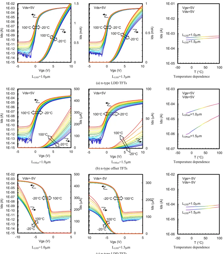
Next, the temperature dependences of the transistor
characteristics are compared between the LDD and offset TFTs. Figure 2 shows the temperature dependences of the transistor characteristics. Here, the relationships between the drain current (Ids) and gate voltage (Vgs) are shown when the drain voltage (Vds) is fixed at 5 V and the temperature (T) is varied from−20◦C to 100◦C, where the vertical axes in the graphs for LLDD or LOffset =1.5µm are the same as those for LLDD or LOffset = 1.0µm and omitted, and the relationships between Ids andT are also shown when Vgs andVds are equal to 5 V for the n-type LDD, n-type offset, and p-type LDD TFTs. The subthreshold swing (S), thresh- old voltage (Vth), and field effect mobility (µ) of the n-type self-aligned TFT, which are not shown in this paper, are 0.279 V·dec−1, 1.03 V, and 67.3 cm2·V−1·s−1, respectively, and those of the p-type self-aligned TFT are 0.215 V·dec−1,
−3.68 V, and 43.7 cm2·V−1·s−1, respectively [14].
Fig. 1 Fabrication processes and device structures of the LDD and offset TFTs.
It is confirmed that the offset TFTs have larger tempera- ture dependence of the on current. The mechanisms why the LDD TFTs have smaller temperature dependence of the on current and the offset TFTs have larger one are as follows. In the case of the LDD TFTs, because the parasitic resistances of the LDD regions are sufficiently low,Idsis mainly deter-
mined by the channel resistances. Although µhas certain temperature dependence, because the carrier densities of the channel regions are governed by Vgs, Ids does not change so much [27]. On the other hand, in the case of the off- set TFTs, because the parasitic resistances of the offset re- gions are considerably high,Idsis mainly determined by the
Fig. 2 Temperature dependences of the transistor characteristics.
parasitic resistances. Because the offset regions are intrin- sic semiconductors and the carrier densities strongly change withT,Ids also changes withT very much. Incidentally, it is difficult to quantitatively measure the parasitic resistances of the offset regions because the parasitic resistances next to the channel regions seem quite different from those in the isolated intrinsic semiconductor patterns owing to the phys- ical behavior.
3. Ring Oscillators
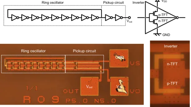
Next, ring oscillators composed of poly-Si TFTs are fab- ricated. The ring oscillators generate spontaneous oscilla- tions, which are subject to the transistor drivability. Fig- ure 3 shows the circuit diagram and microscope photograph of the ring oscillator. Here, static-type ring oscillators con-
sist of the circularly connected odd stages of CMOS invert- ers, which are composed of the n-type LDD and offset TFTs withW =20µm, L =5µm, LLDD = LOffset =1.0µm and p-type LDD TFTs. The supply voltage (Vdd) is applied, the output signal (Vout) is strengthened using the pickup circuit and observed using a high-impedance FET probe, and the oscillation frequency (f) is measured. It seems that f is mainly dependent on the on currents of the LDD and offset TFTs. Therefore, we expect that f is dependent onT.
Finally, the temperature dependences of f are com- pared between ring oscillators using the LDD and offset TFTs. Figure 4 shows the temperature dependence of f. Here, the relationships between f andVdd are shown when T is varied from−10◦C to 100◦C for the ring oscillators us- ing LDD and offset TFTs. The temperature sensitivities of f, which are defined as the ratios between the increase of f fromT =−10◦C to 100◦C and f atT =−10◦C forVdd=
Fig. 3 Circuit diagram and microscope photograph of the ring oscillator.
Fig. 4 Temperature dependence of the oscillation frequencies.
10 V, ( f@100◦C−f@−10◦C )/ f@−10◦C, are also calcu- lated, which are 0.39 and 2.68 for the ring oscillators using LDD and offset TFTs, respectively.
It is found that the ring oscillator using the LDD TFTs has little temperature dependence of f, whereas that using the offset TFTs has larger temperature dependence off ow- ing to the larger temperature dependence of the aforemen- tioned on current. Although we currently have only the ring oscillator composed of the offset TFTs withLOffset=1.0µm, we suppose that the ring oscillator composed of the offset TFTs withLOffset =1.5µm has the comparable or higher sensitivity. In any case, it is clarified that the ring oscillator using the offset TFTs is suitable to detectT. Because the temperature dependence of f is excellently smooth, the de- tection ofT can be extremely precise. The aforementioned sensitivity of 2.68 corresponds to the change of 2.44 % in f per the change of 1◦C inT, which is a sufficient sensitivity for controlling the driving conditions of the display devices.
We think that this kind of temperature sensor is available as a digital device.
4. Conclusion
We proposed a temperature sensor employing a ring oscil- lator composed of poly-Si TFTs. Particularly in this re- search, we compared temperature sensors using LDD and offset TFTs. First, temperature dependences of transistor characteristics were compared between the LDD and offset TFTs. It was confirmed that the offset TFTs have larger tem- perature dependence of the on current. Next, temperature dependences of f were compared between ring oscillators using the LDD and offset TFTs. It was clarified that the ring oscillator using the offset TFTs is suitable to detect the tem- perature. We think that this kind of temperature sensor is available as a digital device. Generally, digital devices are superior to analog devices from the viewpoint of the onward signal operation. It is enough to equip digital pulse counter circuits, which are very simple circuits and easy to be inte- grated on the FPDs using poly-Si TFTs.
Acknowledgments
We thank Y. Hiroshima and M. Miyasaka of Seiko Epson.
This work is partially supported by a collaborative research with Seiko Epson, grant for research facility equipment for private universities from the Ministry of Education, Culture, Sports, Science and Technology (MEXT), grant for special research facilities from the Faculty of Science and Technol- ogy of Ryukoku University, and MEXT-Supported Program for the Strategic Research Foundation at Private Universi- ties.
References
[1] Y. Kuo, Thin Film Transistors, Materials and Processes, 2: Polycrys- talline Silicon Thin Film Transistors, Kluwer Academic Publishers, Boston, 2004.
[2] W. den. Boer, Active Matrix Liquid Crystal Displays: Fundamentals
and Applications. Newnes, Oxford, 2005.
[3] S. Morozumi, K. Oguchi, S. Yazawa, T. Kodaira, H. Ohshima, and T. Mano, “B/W and color LC video display addressed by poly-Si TFTs,” Society for Information Display, 1983 International Sympo- sium (SID ’83), Philadelphia, Digest of Technical Papers, pp.156–
157, 1983.
[4] K. Yoneno, H. Kamakura, J. Nakamura, A. Yajima, J. Karasawa, T.
Nakayama, M. Ogihara, Y. Miyazawa, S. Banda, and N. Okamoto,
“High definition front projector using poly-Si TFT LCD,” Interna- tional Display Research Conference 1991 (IDRC ’91), San Diego, pp.147–150, Oct. 1991.
[5] M. Kimura, I. Yudasaka, S. Kanbe, H. Kobayashi, H. Kiguchi, S. Seki, S. Miyashita, T. Shimoda, T. Ozawa, K. Kitawada, T.
Nakazawa, W. Miyazawa, and H. Ohshima, “Low-temperature polysilicon thin-film transistor driving with integrated driver for high-resolution light emitting polymer display,” IEEE Trans. Elec- tron. Dev., vol.46, no.12, pp.2282–2288, Dec. 1999.
[6] S. Inoue, H. Kawai, S. Kanbe, T. Saeki, and T. Shimoda, “High- resolution microencapsulated electrophoretic display (EPD) driven by poly-Si TFTs with four-level grayscale,” IEEE Trans. Electron.
Dev., vol.49, issue 9, pp.1532–1539, Sept. 2002.
[7] I. Haller and J. D. Litster, “Temperature dependence of normal modes in a nematic liquid crystal,” Phys. Rev. Lett., vol.25, issue 22, pp.1550–1553, Nov. 1970.
[8] E. Liao, J. Peng, and J. Chiu, “Fast switching VA mode LCOS for single panel application,” Society for Information Display, 2005 In- ternational Symposium (SID ’05), Boston, Digest of Technical Pa- pers, vol.36, no.1, pp.1370–1373, May 2005.
[9] G. Vamvounis, H. Aziz, N.-X. Hu, and Z. D. Popovic, “Temperature dependence of operational stability of organic light emitting diodes based on mixed emitter layers,” Synth. Met., vol.143, issue 1, pp.69–
73, May 2004.
[10] J. Kalinowski, Organic Light-Emitting Diodes: Principles, Charac- teristics and Processes, Marcel Dekker, New York, 2005.
[11] A. Nakashima, Y. Sagawa, and M. Kimura, “Temperature sensor using thin-film transistor,” IEEE Sens. J., vol.11, issue 4, pp.995–
998, Apr. 2011.
[12] A. Nakashima, Y. Sagawa, and M. Kimura, “Thermal sensor us- ing poly-Si thin-film transistor with widened detectable temperature range,” IEEE Electron Device Lett., vol.32, no.3, pp.333–335, Mar.
2011.
[13] J. Taya, K. Kojima, T. Mukuda, A. Nakashima, Y. Sagawa, T. Mat- suda, and M. Kimura, “Temperature sensor using poly-Si TFT and 1T1C circuit with gate bias control,” Proc. 20th International Dis- play Workshops (IDW ’13), Sapporo, pp.388–391, Dec. 2013.
[14] J. Taya, A. Nakashima, and M. Kimura, “Thermal sensor employ- ing ring oscillator composed of poly-Si thin-film transistors,” Solid- State Electron., vol.79, pp.14–17, Jan. 2013.
[15] T. Noguchi, H. Hayashi, and T. Ohshima, “Low temperature polysil- icon super-thin-film transistor (LSFT),” Jpn. J. Appl. Phys., vol.25, pt.2 no.2, pp.L121–L123, Feb. 1986.
[16] Y. Mishima, K. Yoskino, F. Takeuchi, K. Ohgata, M. Takei, and N.
Sasaki, “High-performance CMOS circuits fabricated by excimer- laser-annealed poly-Si TFTs on glass substrates,” IEEE Electron De- vice Lett., vol.22, issue 2, pp.89–91, Feb. 2001.
[17] S. D. Brotherton, C. Glasse, C. Glaister, P. Green, F. Rohlfing, and J. R. Ayres, “High-speed, short-channel polycrystalline silicon thin- film transistors,” Appl. Phys. Lett., vol.84, issue 2, pp.293–295, Jan.
2004.
[18] H. Ohshima, Jpn. Patent Application, no.S56–204087, Dec. 1981 (in Japanese).
[19] M. Furuta, Y. Uraoka, and T. Fuyuki, “Reliability of low- temperature poly-Si thin film transistors with lightly doped drain structures,” Jpn. J. Appl. Phys., vol.42, pt.1, no.7A, pp.4257–4260, July 2003.
[20] G. Usami, Y. Nogami, T. Yajima, M. Yamagata, T. Satoh, and H.
Tango, “Hot-carrier degradation and electric field and electron con-
centration near drain junction in low-temperature n-channel single drain and lightly doped drain polycrystalline silicon thin film tran- sistors,” Jpn. J. Appl. Phys., vol.46, pt.1, no.3B, pp.1322–1327, Mar.
2007.
[21] M. Yazakis, S. Takenaka, and H. Ohshima, “Conduction mechanism of leakage current observed in metal-oxide-semiconductor transis- tors and poly-Si thin-film transistors,” Jpn. J. Appl. Phys., vol.31, pt.1 no.2A, pp.206–209, Feb. 1992.
[22] Y. Uraoka, T. Hatayama, T. Fuyuki, T. Kawamura, and Y. Tsuchi- hashi, “Hot carrier effects in low-temperature polysilicon thin-film transistors,” Jpn. J. Appl. Phys., vol.40, pt.1, no.4B, pp.2833–2836, 2001.
[23] Y. Mishima and Y. Ebiko, “Improved lifetime of poly-Si TFTs with a self-aligned gate-overlapped LDD structure,” IEEE Trans. Electron.
Dev., vol.49, issue 6, pp.981–985, June 2002.
[24] A. Valletta, L. Mariucci, A. Pecora, G. Fortunato, J. R. Ayres, and S. D. Brotherton, “A new self-consistent model for the analysis of hot-carrier induced degradation in lightly doped drain (LDD) and gate overlapped LDD polysilicon TFTs,” Thin Solid Films, vol.427, issues 1–2, pp.117–122, Mar. 2003.
[25] M. Miyasaka, T. Komatsu, and H. Ohshima, “Oxidation of amor- phous silicon for superior thin film transistors,” Jpn. J. Appl. Phys., vol.36, pt.1 no.4A, pp.2049–2056, Apr. 1997.
[26] H. Jiroku, M. Miyasaka, S. Inoue, Y. Tsunekawa, and T. Shimoda,
“High-performance polycrystalline silicon thin-film transistors fab- ricated by high-temperature process with excimer laser annealing,”
Jpn. J. Appl. Phys., vol.43, pt.1, no.6A, pp.3293–3296, June 2004.
[27] A. Nakashima and M. Kimura, “Mechanism analysis of off-leakage current in an LDD poly-Si TFT using activation energy,” IEEE Elec- tron Device Lett., vol.32, no.6, pp.764–766, June 2011.
Jun Taya received the B.E. degree in Elec- tronics and Informatics from Ryukoku Univer- sity in 2012. He had been working on tempera- ture sensors composed of poly-Si TFTs.
Kazuki Kojima received the B.E. degree in Electronics and Informatics from Ryukoku Uni- versity in 2014. He had been working on tem- perature sensors composed of poly-Si TFTs.
Tomonori Mukuda received the B.E.
degree in Electronics and Informatics from Ryukoku University in 2013. He had been working on temperature sensors composed of poly-Si TFTs.
Akihiro Nakashima received the B.E.
and M.E. degrees in Electronics and Informat- ics from Ryukoku University in 2008 and 2011, respectively. He had been working on tempera- ture sensors composed of poly-Si TFTs.
Yuki Sagawa received the B.E. degree in Electronics and Informatics from Ryukoku University in 2009, and M. E. degree in Mate- rial Science from Nara Institute of Science and Technologies in 2011. He had been working on chemical sensors and temperature sensors com- posed of poly-Si TFTs.
Tokiyoshi Matsuda received the B.S., M.S., and Ph.D. degrees in Science from Os- aka University in 1997, 2000, and 2003, respec- tively. He joined the University of Sao Paulo as a postdoctoral researcher, Kochi University of Technology in 2004, and Ryukoku University in 2011. He has been working on the research and development of oxide materials for TFT appli- cations.
Mutsumi Kimura received the B.E. and M.E. degrees in Physical Engineering from Ky- oto University in 1989 and 1991, respectively, and the Ph. D. degree in Electrical and Elec- tronic Engineering from Tokyo University of Agriculture and Technology in 2001. He joined Matsushita Electric Industrial Co., Ltd. in 1991, Seiko Epson Corp. in 1995, and Ryukoku University in 2003. He has been working on TFT characteristic analysis, TFT simulator de- velopment, TFT-OLED development, and their advanced applications.