598
IEICE TRANS. ELECTRON., VOL.E98–C, NO.7 JULY 2015
INVITED PAPER
Special Section on Microwave and Millimeter-Wave TechnologyRecent Advances in Microwave Planar Filter Technology
Jiasheng HONG†a), Jia NI†, Francisco CERVERA†,andLaura HEPBURN†,Nonmembers
SUMMARY This invited paper aims to present an overview of our re- cent research and development (R&D) of advanced microwave planar fil- ters, in particular with miniaturization and/or electronically tunable/re- configurable functionalities, which are in demand for future communica- tion/radar systems as well as emerging wireless applications.
key words: microwave filters, planar filters, multilayer filters, tunable fil- ters, reconfigurable filters
1. Introduction
Recently, there is an increasing demand for miniature and/or tunable/reconfigurable microwave planar filters. For the filter miniaturization, we have exploited multilayer liquid crystal polymer (LCP) technology[1]–[11]. LCP has been popular not only due to its superior electrical properties up to millimeter-wave frequencies[12], but also because itself is an excellent packaging material for system-on- package[13]. It has a stable low dielectric constant around 3 and low dielectric loss tangent 0.0025 over a wide frequency range. Compared to LTCC, LCP has much lower process- ing temperature around 280◦C. Although LCP has lower dielectric constant than LTCC, which makes it more chal- lenging for RF/Microwave circuit miniaturization, it makes LCP circuit design less sensitive to fabrication tolerances than LTCC, which is very important for multilayer lami- nated circuit. Although some cheaper PCB laminates can be used for miniature filter designs, LCP offers much higher flexibility on circuit thickness and a very strong coupling can be achieved with a separation as small as 25μm. This is very important for the design of low frequency filters that re- quires large capacitances. Furthermore, in the LCP adhesive system[14], circuit layers (core films) and prepreg layers (bonding films) have almost the same characteristics, such as thermal expansion coefficient, dielectric constant and wa- ter absorption, which can be a great benefit for both filter designs and practical applications.
In addition to the filter miniaturization, electronically tunable or reconfigurable filters are also in increasing de- mand in current and emerging multifunctional communi- cation and radar systems owning to their efficiency in use and flexibility in control of frequency spectrum. In general, to develop an electronically tunable or reconfigurable filter,
Manuscript received April 2, 2015.
†The authors are with Institute of Sensors, Signals & Systems, School of Engineering and Physical Sciences, Heriot-Watt Univer- sity, Edinburgh, UK.
a) E-mail: [email protected] DOI: 10.1587/transele.E98.C.598
active switching or tuning elements such as semiconduc- tor p-i-n and varactor diodes, RF microelectromechanical systems (MEMS) or other functional material-based com- ponents including ferroelectric capacitors need to be inte- grated within a passive filtering structure[15]. Planar fil- ters can conveniently facilitate this kind of integration with a small size and to this end we have carried out R&D for tunable or reconfigurable planar filters are based on planar structures[16]–[33].
In the following parts, several typical advanced planar filters resulting from our R&D are highlighted.
2. Packaged LCP Filters
This section is to demonstrate the methods for integrating filters within a package as one of the stages in the manufac- turing process, using LCP multilayer technology. Including the packaging in the manufacturing process will reduce the number of processes needed and thus, the final cost of the solution.
2.1 Hermetic Packaged UWB Filter
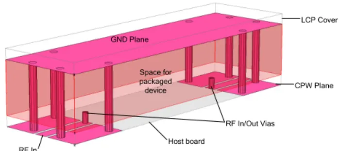
The concept for packaging with CPW input/output (I/O) ports is illustrated in Fig. 1, which consists of two layers of LCP substrate holding the packaged device in between. The bottom layer will interface between the host board and the packaged device through a CPW structure. Since the CPW structure has both signal and ground on the same plane, it will simplify the connection of the device to the host board.
On the other side, the top layer is the ground plane for both the CPW structure and the packaged device. In this way, the CPW becomes grounded-CPW (G-CPW). However, to sim- plify, G-CPW will be referred as CPW in this paper. CPW and ground plane are connected through via-holes. On top
Fig. 1 Main concept for packaging with CPW input/output (I/O) ports.
Copyright c2015 The Institute of Electronics, Information and Communication Engineers
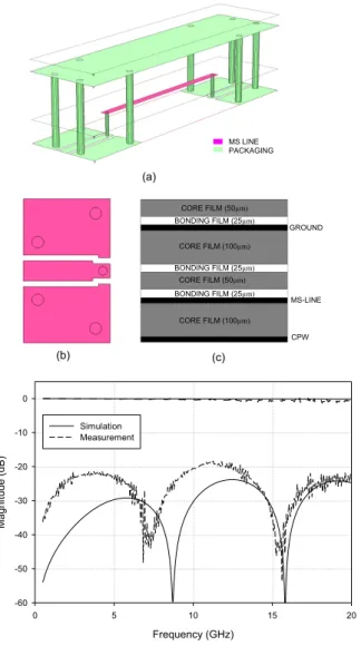
Fig. 2 (a) 3D view of Thru-Line design (b) Modified CPW structure (c) Layer stack (d) Simulation and measurement results for Thru-line experi- ment.
of the ground layer, an extra layer of LCP is placed to com- plete the hermetic packaging.
For the purpose of measuring the losses the package in- troduces and how it affects the bandwidth, a contained mi- crostrip (MS) end-to-end line was fabricated (Fig. 2). Dur- ing a lamination process misalignment in the inner layers may arise due to the bonding film melting. In order to mini- mize this effect, for this experiment CPW and MS line were etched in the same double-sided substrate (Fig. 2 (c)). Re- sults measured after fabrication show a reasonable agree- ment with the EM simulation[33]. The insertion loss is less than 1.5 dB and the return loss, better than 18 dB in a fre- quency span of 0.5 to 20 GHz (Fig. 2 (d)).
This packaging technique is applied to an integrated UWB filter as shown in Fig. 3. The UWB filter is imple- mented in layers 1 and 2 (refer to Fig. 3 (b)), which consists of quasilumpedLCelements. For the design of the CPW, parameters G and W are set to match 50Ωimpedance. The
Fig. 3 (a) 3D view of UWB packaged filter (b) Layer stack (c) Measured results of the fabricated UWB filter with hermetic packaging.
packaged filter was fabricated. It has a size of 10 mm by 16.8 mm including 3 mm long CPW feed line at each. The thickness of the packaged filter is only 0.7 mm. The fabri- cated UWB filter and its measured response are illustrated in Fig. 3 (d).
2.2 Self-Packaged Dual-Band Filter
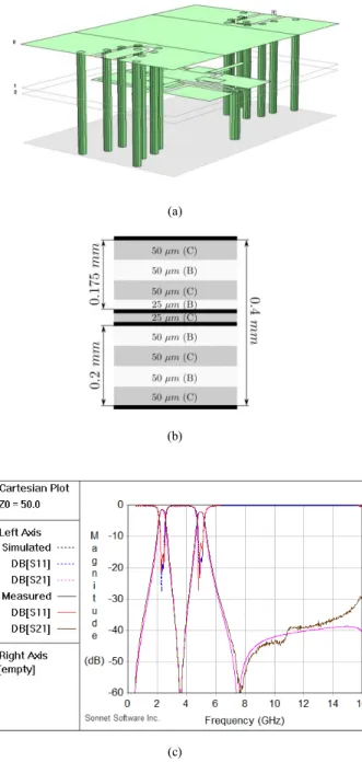
Another developed self-packaged dual-band filter is demon- strated in Fig. 4. The multilayer structure consists of four metal layers. On the central layer, two coupled dual-mode resonators are placed next to each other in a mirrored dis- position. The coupling between them is produced by this proximity between them as well as a pair of metal patches,
600
IEICE TRANS. ELECTRON., VOL.E98–C, NO.7 JULY 2015
placed on the layer above them, that controls the coupling coefficients for each of the passbands. The coupling be- tween the resonators and the input/output ports is achieved by a second pair of patches whose area determines the ex- ternal quality factor (Qe) for each band. The top and bottom layers are the ground planes, also providing electromagnetic shielding to the filter. Furthermore, the top layer contains a pair of coplanar waveguide (CPW) lines that connect the filter to the external environment through a vertical via tran- sition. The whole packaged filter is implemented using liq- uid crystal polymer (LCP) material (refer to Fig. 4 (b)). The dual-band design is aiming at 2.4/5 GHz WiFi bands with
Fig. 4 (a) 3D view of self-packaged dual-band filter (b) Layer stack (C=Core LCP film; B=Bonding LCP film) (c) Simulated and measured responses of the self-packaged dual-band filter.
fractional bandwidths of 8% and 5%, respectively. The de- signed filter has a footprint of 7.5 mm×11.2 mm with a low profile of 0.4 mm, including the self-packaging. Fig- ure 4 (c) plots the measured response along with the simu- lated one, obtained by Sonnet EM[33], showing promising results with good agreement.
3. Quasi-Lumped-Element LCP Filters
In this section, two typical miniature filters consisting of quasi-lumped elements that are directly implemented in multilayer LCP structure are highlighted.
3.1 VHF-band Bandpass Filter
For this work, a four-pole bandpass filter is designed with a center frequency of 250 MHz and equal ripplefractional bandwidth(FBW) of 20%. Figure 5 illustrates the proposed realization of this multilayer LCP bandpass filter based on a lumped element circuit model. Based on the circuit model, the multilayer LCP design is produced as a compact imple- mentation. The multilayer LCP structure has a total thick- ness of 0.4mm, and the dielectric constant and loss tan- gent is 3 and 0.0025 respectively. The structure consists of 4 copper layers for the circuit patterns and one for the ground. The separation between every two adjacent circuit layers is 50μm to provide a high capacitance density for the multilayer capacitors. The conductivity of the copper is 5.8×10⁷S/M.
A sample for this design has been fabricated, as shown in Fig. 6 (a). Excluding the 50 Ohm feed line, the filter has a size of 56.7mm×13.75mm×0.4mm, which is only 0.074λg×0.018λg×0.00052λg, whereλgis the guided wave- length at the center frequency 250 MHz. The sample with SMA connectors is measured. The measured S parameters are shown in Fig. 6 (b). As can be seen, the measurement is in good agreement with the EM simulation[33]in terms of the bandwidth, stopband attenuation and the frequency of the 2ndharmonic. The stopband performance is excellent
Fig. 5 (a) Proposed multilayer LCP bandpass filter and (b) its equivalent lumped element circuit model.
Fig. 6 (a) A Photo of the fabricated VHF-band LCP filter (b) Compari- son between measurement and simulation.
Fig. 7 (a) 3-D structure for the UHF-band LCP filter (not on scale) (b) Its equivalent lumped-element circuit model.
with a high rejection down to 70dB, which is already around the noise floor. The 2nd harmonic only appears at about 9.4 times the center frequency and is below−36dB.
Fig. 8 (a) Fabricated UHF-band LCP filter (b) Measured results.
3.2 UHF-Band Bandpass Filter
The second miniature filter is designed to operate at a UHF-band with a fractional bandwidth of 20% cantered at 500 MHz. Figure 7 depicts the multilayer structure of the filter and its equivalent lumped-element circuit model.
The multilayer structure is comprised of three metal layers on the top and a metal ground plane on the bot- tom, supporting by total seven 50um-thick layers of LCP substrates. The top three metal layers with a separation of 50 um from adjacent ones are used to implement the quasi- lumped elements. The distance from the third metal layer to the ground is 250 um. Thus the designed multilayer filter has a very low profile (∼0.35mm) with a small active circuit footprint of 22.9mm x 10.4mm. A fabricated filter sample and its measured results are shown in Fig. 8.
4. Tunable/Reconfigurable Filters
4.1 Tunable Filter with Improving Passband Flatness In general, any tuning elements used in the realization of electrically tunable filter add losses to the filter, which, as a result, degrades the performance of tunable filters. This is seen particularly as an increased in passband insertion loss and a rounding of the passband edges leading to a poorer selectivity, which become more pronounced in narrowband filters. Although for some applications the absolute inser- tion loss can be tolerated, a flatter tunable passband would be required. We have investigated the performance enhance- ment for the passband flatness and selectivity of tunable fil- ters by reducing the resonator unloadedQto get an optimal Qdistribution. For this investigation, the configuration of
602
IEICE TRANS. ELECTRON., VOL.E98–C, NO.7 JULY 2015
Fig. 9 Tunable combline filter concept with improved performance.
Fig. 10 (a) Fabricated tunable filter with improving passband flatness and selectivity (b) Measured results.
a proposed third-order tunable combline filter with biasing scheme is shown in Fig. 9, which consists of three short- ended quarter-wavelength resonators with varactor diodes Cvfor central frequency tuning, whererrepresents the var- actor loss.Cdis the bypass or dc block capacitor. Rd is the dc bias resistor. The capacitorCplaced at middle resonator is utilized for a desired detuning, and the resistorR added at each resonator is used to manipulate the resonator’s un- loadedQfactor. In addition, there are two shunt resistors (R0) located at input and output (I/O) ports to improve the return loss and selectivity to some extent.
For the experimental demonstration, Fig. 10 illustrates the fabricated tunable microstrip combline filter and its mea- sured performance with enhanced passband flatness and se- lectivity. The substrate used is RT/Duriod 6010 withεr =
Fig. 11 (a) Concept of channel reconfigurable filter based on bi-modal stages and (b) A practical implementation with two stages for 4 channel states. (c) S21 of 4 channels from full-wave EM simulation.
10.2 and h = 1.27 mm. The values of the added lumped element components for the performance enhancement are C =0.1 pF,R=2000ΩandR0 =300Ω, respectively. The GaAs varactor diodes MA46H202 are used for tuning. The measured results are obtained for DC bias voltage varying from 10.0 to 22.0 V. NormalizedS21 response (measured) of the upper channel of the proposed tunable combline fil- ter indicates the improved passband flatness and selectivity with an equivalentQof 340, which is much higher than the actualQ.
4.2 Channel Reconfigurable Filter
Shown in Fig. 11 (a) is a general concept of the n-stage struc- ture of the cascaded channel reconfigurable filter. In this type of filter, every stage is able to be configured as a high- pass or lowpass filter. Then by overlapping different high- pass and lowpass response, different channels can be real- ized. For an n-stage filter, 2nchannels can be realized. As a preliminary demonstration, a filter with two stages based on stripline realization is depicted in Fig. 11 (b) with the full-
Fig. 12 (a) Multilayer LCP stripline circuit with integrated MMIC switch (b) Fabricated reconfigurable filter (c) Measured S21 of the 4 chan- nels.
wave EM simulated 2-stage response with 4 channels cov- ering the frequency range from DC to 4GHz as shown in Fig. 11 (c).
With multilayer liquid crystal polymer (LCP) technol- ogy, stripline structure can be easily constructed as shown in Fig. 12 (a). To connect the top and bottom grounding layer together for a stripline configuration, connection vias are drilled by picoseconds laser and then plated by high con- ductivity paste using through-hole plating technique. For the whole filter, both of the bi-modal stages and the switch- ing network are fabricated together as a single LCP package, as shown in Fig. 12 (b), which has a planar size of 4.3 cm× 3.6 cm. The embedded filter layout is similar to that shown in Fig. 11 (b). Then, by using high precision picoseconds laser, a window can be opened and thus the DPDT switch can be easily integrated into the LCP package. Measured S parameters are shown in Fig. 12 (c). It can be seen that due to non-dispersive stripline configuration, the periodicity of the filter is well maintained. Since the absolute bandwidth is constant, the fractional bandwidth is then reduced while the
Fig. 13 (a) Circuit model for the reconfigurable filter having three recon- figurable bandwidth states (50%, 40% and 30%). (b) Circuit response of S21. (c) Circuit response of S11.
insertion loss increased from the state 1 to state 4. Neverthe- less, the loss of filter is reasonably small. The DPDT switch being used in this work is the MA-Com MASWSS0129 broadband DPDT GaAs MMIC switch.
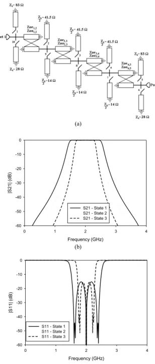
4.3 Coupled Line Filter with Reconfigurable Bandwidths Figure 13 (a) is a circuit model for the reconfigurable filter having three reconfigurable bandwidth states. The circuit is basically a coupled line filter with switchable short-circuited stubs having different characteristic impedances. Without
604
IEICE TRANS. ELECTRON., VOL.E98–C, NO.7 JULY 2015
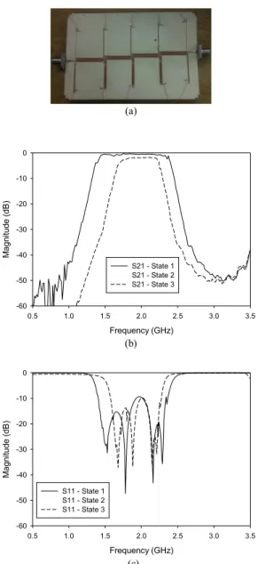
Fig. 14 (a) Fabricated reconfigurable filter having three reconfigurable bandwidth states. (b) Measured response of S21. (c) Measured response of S11.
the switchable stubs, the reconfigurable filter is operated at a state of the desired largest bandwidth and in this case it is designed to have 50% fractional bandwidth. For a 40% frac- tional bandwidth, a stub impedance of 83Ωis required, and for a 30% fractional bandwidth, an impedance of 28Ωis re- quired. For this demonstration, all line lengths areθ=90◦at the center frequency of 2 GHz. Figures 13 (b) and (c) show the circuit modeling responses of S21 and S11 respectively.
The three states are achievable by the following switching arrangement for each state:
• 50% - all switches turned off.
• 40% - switches 1, 2, 3, 4, and 5.
• 30% - switches 6, 7, 8, 9, and 10.
The designed filter circuit was implemented using LCP mul- tilayer circuit technology to facilitate embedded floating
Fig. 15 Concept for realizing reconfigurable filter with tunable band- width and central frequency.
metal strip for a broadside coupling arrangement in order to obtain the desired coupling. PIN diodes (MA/COM’s MA4AGBLP912) are deployed for switching on/off the short circuit stubs. A photograph of the fabricated filter is illustrated in Fig. 14 (a). The measured filter responses including the out-of-band spurious are demonstrated in Figs. 14 (b) and (c), showing the effective bandwidth tuning.
4.4 Filter with Tunable Bandwidth and Central Frequency To tune both bandwidth and central frequency, an useful concept is illustrated in Fig. 15, which is based on the com- bination of tunable bandpass filter (BPF) and lowpass filter (LPF) modules in cascade. As can be seen, variable cen- tre frequency and bandwidth can be flexibly achieved by controlling the tunable BPF or LPF individually or jointly.
Specifically, tunable BPF and LPF modules are mostly asso- ciated with the filter shape at the lower and the upper band, respectively. Consequently, the tunable performance of each module adopted in the topology is very critical to get a good final response. Particularly, for the narrow bandwidth real- ization during the tuning process, it requires each module providing a very sharp bandedge frequency response to ob- tain a good matching within the passband.
Figure 16 (a) shows the design layout for such a re- configurable filter, which is implemented by using LCP bonded multilayer PCB technology. GaAs varactor diode MA46H120 (0.17–0.9pF, and Q = 3000 forVR = 4V at f = 50MHz) and silicon abrupt junction varactor diode SMV1800-079LF (0.84–15.78pF, and Rs = 3Ω for VR = 1.5V at f =470MHz) are adopted for tuning. Figure 16 (b) illustrates the fabricated reconfigurable filter with a test fix- ture for measurement. Four dc biases are required for this reconfigurable filter, namely V1 and V2 for the BPF module on the left and V3 and V4 for the LPF module on the right.
Figure 17 demonstrates several typical tuning perfor- mance of the developed reconfigurable filter. For instance, in Fig. 17 (a), when keeping the applied voltages V3 and V4 fixed at 5V, increasing the voltages V1, V2 of BPF mod-
Fig. 16 Implementation of reconfigurable filter with tunable bandwidth and central frequency. (a) Design layout (All dimensions are in millime- ters). (b) Fabricated reconfigurable filter with a test fixture for measure- ment.
ule from 0V, 0V to 10V, 15V results in the lower passband edge is tuned upwardly toward the high end frequency from 1.17 to 2.01 GHz, with measured minimum insertion loss varying from 1.6 to 3.3 dB. Similarly, by only adjusting the voltages V3, V4 from 5V, 5V to 20V, 20V, while keeping V1 and V2 fixed at 10 and 15 V respectively, as indicated in Fig. 17 (b), the upper passband edge can be shifted from 2.22 to 3.17 GHz, with measured minimum insertion loss chang- ing from 3.3 to 1.2 dB. Furthermore, when four applied volt- ages are controlled simultaneously, it is clear from the re- sults of Fig. 17 (c) that both of passband edges are moved toward to the centre frequency (around 2GHz), which re- sults in the corresponding 3 dB bandwidth changing from 1.78 to 0.26 GHz with a minimum measured insertion loss of 1.1 and 4.9 dB, respectively. The bandwidth tuning ratio is up to 6.85:1. In fact, this bandwidth controlling capabil- ity can be further improved at the expense of higher inser- tion loss suffered in the narrow passband. Hence, there is a tradeoffbetween the insertion loss and bandwidth tunabil- ity. Technically, the filter can provide a bandwidth variance from wideband to narrowband at any operating frequency with both high selectivity and good matching.
5. Conclusion
In this overview paper, several advanced microwave pla- nar filters have been highlighted including the LCP pack- aged UWB and dual-band filters, miniature quasi-lumped element filters based on multilayer LCP technology, tun- able filter with improving passband flatness, channel- reconfigurable filter, reconfigurable bandwidth filter and re- configurable filter with both bandwidth and central fre-
Fig. 17 Demonstration of reconfigurable filter responses obtained by controlling (a) Sole BPF module. (b) Sole LPF module. (c) Both mod- ules.
quency tuning. To meet the stringent requirements on size/weight, cost, performance and functionality for future system applications, there are still challenges for R&D of microwave planar filter technology.
Acknowledgments
The authors would like to thank Dr. A. Miller and Dr. S.
Qian, the former PhD students in RF/microwave research group at Heriot-Watt University, for their contributions to
606
IEICE TRANS. ELECTRON., VOL.E98–C, NO.7 JULY 2015
some work highlighted in this paper.
References
[1] J.-S. Hong, Microstrip Filters for RF/Microwave Applications, 2nd ed., Wiley, New Jersey, 2011.
[2] Z.-C. Hao and J.-S. Hong, “Ultra-Wideband Bandpass Filter Using Multilayer Liquid-Crystal-Polymer Technology,” IEEE Trans. Mi- crow. Theory Tech., vol.56, no.9, pp.2095–2100, Sept. 2008.
[3] Z.-C. Hao and J.-S. Hong, “Compact Wide Stopband Ultra Wide- band Bandpass Filter Using Multilayer Liquid Crystal Polymer Technology,” IEEE Microw. Wireless Compon. Lett., vol.19, no.5, pp.290–292, May 2009.
[4] Z.-C. Hao and J.-S. Hong, “UWB Bandpass Filter Using Cascaded Miniature High-Pass and Low-Pass Filters With Multilayer Liquid Crystal Polymer Technology,” IEEE Trans. Microw. Theory Tech., vol.58, no.4, pp.941–948, April 2010.
[5] Z.-C. Hao and J. Hong, “Multilayer interdigital ultra-wideband fil- ter,” International Microwave Symposium Digest (IMS2011), 2011.
[6] S. Qian and J. Hong, “Miniature Quasi-Lumped-Element Wideband Bandpass Filter at 0.5–2-GHz Band Using Multilayer Liquid Crystal Polymer Technology,” IEEE Trans. Microw. Theory Techn., vol.60, no.9, pp.2799–2807, 2012.
[7] F. Cervera, J. Hong, and N. Thomson, “Development of pack- aged UWB passive devices using LCP multilayer circuit technol- ogy,” 42nd European Microwave Conference (EuMC), pp.1150–
1153, 2012.
[8] S. Qian and J.-S. Hong, “A compact multilayer liquid crystal poly- mer VHF bandpass filter,” 43rd European Microw. Conf., pp.1207–
1210, Oct. 2013.
[9] S. Qian, J.-S. Hong, A. Rusakov, and I.B. Vendik, “A Novel Compact Ultra-Wideband Bandpass Filter,” 43rd European Microw.
Conf., pp.896–899, Oct. 2013.
[10] F.J. Cervera and J. Hong, “Compact Self-Packaged Dual-Band Filter Using Multilayer Liquid Crystal Polymer Technology,” IEEE Trans.
Microw. Theory Techn., vol.62, no.11, pp.2618–2625, 2014.
[11] L. Hepburn and J. Hong, “On the development of compact lumped-element LCP filters,” 44th Microwave Conference (EuMC), pp.544–547, 2014.
[12] D.C. Thompson, O. Tantot, H. Jallageas, G.E. Ponchak, M.M.
Tentzeris, and J. Papapolymerou, “Characterization of liquid crys- tal polymer (LCP) material and transmission lines on LCP substrate from 30–100 GHz,” IEEE Trans. Microw. Theory Tech., vol.52, no.4, pp.1343–1352, April 2004.
[13] K. Brownlee, S. Bhattacharya, K. Shinotani, C.P. Wong, and R.
Tummala, “Liquid crystal polymer for high performance SOP appli- cations,” in 8th IEEE Int. Adv. Packag. Mater. Symp., pp.249–253, March 3–6, 2002.
[14] Fabrication Guidelines ULTRALAM-3000-LCP-Materials, Rogers Corporation, Connecticut, USA, 2012.
[15] J.-S. Hong, “Reconfigurable Planar Filters,” IEEE Microwave Mag., pp.73–83, Oct. 2009.
[16] Y.-H. Chun, J.-S. Hong, P. Bao, T.J. Jackson, and M.J. Lancaster,
“BST-Varactor Tunable Dual-Mode Filter Using Variable ZC Trans- mission Line,” IEEE Microw. Wireless Compon. Lett., vol.18, no.3, pp.167–169, 2008.
[17] Y.-H. Chun, J.-S. Hong, P. Bao, T.J. Jackson, and M.J. Lancaster,
“Tunable Slotted Ground Structured Bandstop Filter with BST Var- actors,” IET Proceedings, Microwaves Antennas & Propagation, vol.3, no.5, pp.870–876, Aug. 2009.
[18] Z.-C. Hao and J.-S. Hong, “UWB Bandpass Filter with Switchable Notching Band using Multilayer LCP Technology,” 40th European Microwave Conference EuMC 2010, 2010.
[19] A. Miller and J.-S. Hong, “Wideband Bandpass Filter with Multiple Reconfigurable Bandwidth States,” 40th European Microwave Con- ference, EuMC2010.
[20] W. Tang and J.-S. Hong, “Microstrip Quasi-Elliptic Function Band-
pass Filter with Improved Tuning Range,” 40th European Mi- crowave Conference, EuMC2010.
[21] W. Tang and J.-S. Hong, “Varactor-Tuned Dual-Mode Bandpass Fil- ters,” IEEE Trans. Microw. Theory Techn., MTT-58, vol.58, no.8, pp.2213–2219, 2010.
[22] A. Miller and J.-S. Hong, “Wideband Bandpass Filter With Recon- figurable Bandwidth,” IEEE Microw. Compon. Lett., vol.20, no.1, pp.28–30, Jan. 2010.
[23] M.A. Sanchez-Soriano and J.-S. Hong, “Reconfigurable lowpass fil- ter based on signal interference techniques,” 2011 IEEE Interna- tional Microwave Symposium Digest (IMS2011), pp.1–4, 2011.
[24] W. Tang and J. Hong, “Reconfigurable Microstrip Combline Filter with Tunable Center Frequency and Bandwidth,” APMC2011.
[25] A. Miller and J.-S. Hong, “Reconfigurable cascaded coupled line filter with four distinct bandwidth states,” IET Microw. Antennas Propag., vol.5, no.14, pp.1730–1737, 2011.
[26] J. Ni, W. Tang, Z.-C. Hao, and J. Hong, “An Investigation of Per- formance Enhancement for Tunable Microstrip Filter,” Proc. 41st European Microwave Conference, Oct. 2011.
[27] A. Miller and J. Hong, “Cascaded Coupled Line Filter With Recon- figurable Bandwidths Using LCP Multilayer Circuit Technology,”
IEEE Trans. Microw. Theory Techn., vol.60, no.6, pp.1577–1586, June 2012.
[28] A. Miller and J. Hong, “Electronically reconfigurable multi-chan- nel wideband bandpass filter with bandwidth and centre frequency control,” IET Microwaves, Antennas & Propagation, vol.6, no.11, pp.1221–1226, 2012.
[29] S. Qian and J. Hong, “Channel-reconfigurable filter with integrated switch in multilayer LCP package,” 42nd European Microwave Con- ference (EuMC), pp.265–268, 2012.
[30] J. Ni and J. Hong, “Compact Continuously Tunable Microstrip Low-Pass Filter,” IEEE Trans. Microw. Theory Techn., vol.61, no.5, pp.1793–1800, May 2013.
[31] J. Ni and J. Hong, “Compact Varactor-Tuned Microstrip High-Pass Filter with a Quasi-Elliptic Function Response,” IEEE Trans. Mi- crow. Theory Techn., vol.61, no.11, pp.3853–3859, Nov. 2013.
[32] J. Ni and J. Hong, “Varactor-Tuned Microstrip Bandpass Filters with Different Passband Characteristics,” Microwaves, Antennas & Prop- agation, IET, vol.8, no.6, pp.415–422, April 2014.
[33] “EM User’s Manual,” ver. 12, Sonnet Software Inc., Syracuse, NY, 2010.
Jiasheng Hong received the D.Phil. degree in engineering science from the University of Oxford, UK, in 1994. His doctoral dissertation concerned EM theory and applications. In 1994, he joined the University of Birmingham, UK, where he was involved with microwave applica- tions of high temperature superconductors, EM modeling, and circuit optimization. In 2001, he joined the Department of Electrical, Electronic and Computer Engineering, Heriot-Watt Univer- sity, Edinburgh, UK, and is currently a professor leading a team for research into advanced RF/microwave device technolo- gies. He has authored and coauthored over 200 journal and conference papers, and also two books,Microstrip Filters for RF/Microwave Appli- cations(New York: Wiley, 1stEdition 2001, 2nd Edition 2011) andRF and Microwave Coupled-Line Circuits, Second Edition(Boston: Artech House, 2007). His current interests involve RF/microwave devices, such as antennas and filters, for wireless communications and radar systems, as well as novel material and device technologies including multilayer circuit technologies using package materials such as liquid crystal polymer, RF MEMS, ferroelectric and high temperature superconducting devices. Prof.
Hong is a fellow of IEEE.
Jia Ni was born in Hunan, China, in 1986.
She received the B.Eng. degree in electrical en- gineering from the Nanjing University of Sci- ence and Technology, Nanjing, China, in 2008, and the PhD degree from Heriot-Watt Univer- sity, Edinburgh, U.K., in 2014 Her research in- terests include tunable and reconfigurable mi- crowave filters, multilayer circuit design, and miniature RF/microwave devices.
Francisco J. Cervera received the B.Eng. degree in Telecommunications Engi- neering from Universidad Europea de Madrid, Madrid, Spain, in 2007, and MSc in Mo- bile Communications from HeriotWatt Univer- sity, Edinburgh, U.K. Currently working to- wards the Ph.D. degree at School of Engineering and Physical Sciences, Heriot Watt University.
His research interests include miniature, self- packaged, multilayer RF/microwave filters us- ing LCP materials, and integration for wireless communication and radar systems.
Laura Hepburn received the MEng de- gree in Electrical and Electronic Engineering from Heriot-Watt University, Edinburgh, U.K., in 2013. Since July 2013, she has been a PhD student at the same university carrying out re- search into miniature multilayer microwave fil- ters.