象VHH内蔵の250MHzデュアルDCL
ADATE305
アナログ・デバイセズ社は、提供する情報が正確で信頼できるものであることを期していますが、その情報の利用に 関して、あるいは利用によって生じる第三者の特許やその他の権利の侵害に関して一切の責任を負いません。また、 アナログ・デバイセズ社の特許または特許の権利の使用を明示的または暗示的に許諾するものでもありません。仕様特長
ドライバ クランプ機能内蔵の高 Z モード 3 レベル・ドライバ 調整済みの高精度出力抵抗 低リーク・モード: 10 nA 以下 (typ) 電圧範囲: −2.0 V~+6.0 V 最小パルス幅: 1.6 ns、2 V 終端 最小パルス幅: 2.1 ns、3 V 終端 コンパレータ ウインドウおよび差動コンパレータ 入力等価帯域幅: 500 MHz 負荷 最大電流能力: ±12 mA ピンごとの PMU 電圧フォース範囲: −2.0 V~+6.0 V5 種類の電流範囲: 32 mA、2 mA、200 µA、20 µA、2 µA レベル DCL レベル用の 14 ビット DAC INL: ±5 mV 以下 (Typ 値、キャリブレート済み) PMU レベル用の 16 ビット DAC INL 直線性: FV モードで±1.5 mV 以下(Typ 値、キャリブレート 済み) 出力バッファ付きの HVOUT 出力範囲: 0 V~13.5 V 100 ピンの 14 mm × 14 mm TQFP_EP パッケージを採用 無負荷時チャンネルあたり 900 mW
アプリケーション
自動テスト装置 半導体テスト・システム ボード・テスト・システム 計装装置およびキャラクタライゼーション装置概要
ADATE305 は、ドライバ・ピンの電気的機能、コンパレータ、 アクティブ負荷(DCL)、ピンごとの PMU、ATE アプリケーション での DC レベル機能を実行するシングルチップ・ソリューション です。このデバイスには、最大 13.5 V の VHH バッファ能力を 持つ HVOUT ドライバも内蔵されています。 このドライバは、データ・ハイ・モード、データ・ロー・モー ド、終端モードの 3 つのアクティブ状態と、さらにインヒビッ ト状態を持っています。インヒビット状態と内蔵のダイナミッ ク・クランプの組み合わせにより、高速なアクティブ終端が可 能になります。ADATE305 は、正と負の電源電圧を調節するこ とにより、−2.0 V~+6.0 V と−1.5 V~+6.0 V の 2 つの出力電圧範 囲をサポートします。 ADATE305 は、2 系統のシングルエンド駆動/受信チャンネルま たは 1 系統の差動駆動/受信チャンネルとして使うことができま す。ADATE305 の各チャンネルには、ピンごとに機能テスト用 の高速ウインドウ・コンパレータが付いており、さらに FV 機 能、または FI 機能と MV 機能、または MI 機能を持つ PMU が ピンごとに付いています。DCL 機能に必要なすべての DC レベ ルは、内蔵の 14 ビット DAC で発生されます。ピンごとの PMU は、高精度の 16 ビット DAC と外付け部品数を減らすためのレ ンジ抵抗を内蔵しています。 ADATE305 は、シリアル・バスを使ってすべての機能ブロック を設定し、デバイス温度モニター用の温度センサーを内蔵して います。目次
特長 ... 1 アプリケーション ... 1 概要 ... 1 改訂履歴 ... 2 機能ブロック図 ... 3 仕様 ... 4 全体機能 ... 4 ドライバ ... 5 反射のクランプ ... 7 ノーマル・ウインドウ・コンパレータ... 7 差動コンパレータ ... 9 アクティブ負荷 ... 11 PMU ... 12 外部検出(PMUS_CHx) ... 16 DUTGND 入力 ... 17 シリアル・ペリフェラル・インターフェース ... 18 HVOUT ドライバ ... 18 過電圧検出器(OVD) ... 19 16 ビット DAC モニター・マルチプレクサ ... 19 絶対最大定格 ... 20 熱抵抗 ... 20 テスト・レベルの説明 ... 20 ESD の注意 ... 20 ピン配置およびピン機能説明 ... 21 代表的な性能特性 ... 24 SPI の詳細 ... 35 SPI 用語の定義 ... 36 書き込み動作 ... 37 読み出し動作 ... 38 リセット動作 ... 39 レジスタ・マップ ... 40 レジスタの詳細 ... 41 ユーザ情報 ... 43 DAC 対レベルの詳細... 45 PMU モード・スイッチングの推奨シーケンス ... 48 ブロック図 ... 51 外形寸法 ... 55 オーダー・ガイド ... 55改訂履歴
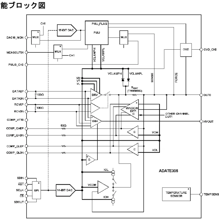
機能ブロック図
仕様
キャラクタライゼーションと出荷テストは電源範囲 1 (表 36)を使って実施。VDD = +10.0 V、VCC = +3.3 V、VSS = −5.25 V、VPLUS = +16.75 V、
VCOMP_VTT = +3.3 V、VREF = +5.0 V、VREF_GND = 0.0 V。すべてのデフォルト・テスト条件は表 38 に規定。特に指定のない限り、すべての仕
様値は TJ = 70°C で規定。TJは内部温度センサーに対応。特に指定のない限り、温度係数は TJ = 70°C ± 20°C で測定。Typ 値は、デザイン、
シミュレーション解析、および/または限られたベンチ評価に基づきます。Typ 値はテストしません。または保証しません。テスト・レベ ルは、テスト・レベルの説明のセクションで規定します。
全体機能
表 1.
Parameter Min Typ Max Unit Test
Level Conditions/Comments
TOTAL FUNCTION Output Leakage Current
PE Disable Range E −20.0 5.3 +20.0 nA P −1.5 V < VDUTx < +6.0 V; PMU and PE disabled via SPI; PMU
Range E, VCH = 7.0 V, VCL = −2.5 V
PE Disable Range A, B, C, D 5.3 nA CT −1.5 V < VDUTx < +6.0 V; PMU and PE disabled via SPI; PMU
Range A, PMU Range B, PMU Range C, and PMU Range D, VCH = +7.0 V, VCL = −2.5 V
High-Z Mode −400 5.4 +400 nA P −1.5 V < VDUTx < +6.0 V; PMU disabled and PE enabled via
SPI; RCV active, VCH = +7.0 V, VCL = −2.5 V
Output Capacitance 4 pF S VTERM mode operation
DUT Pin Range −1.5 +6.0 V D
POWER SUPPLIES
Total Supply Range, VPLUS to VSS 22.5 23.25 V D Defines PSRR conditions
VPLUS Supply, VPLUS 16.25 16.75 17.25 V D Defines PSRR conditions
Positive Supply, VDD 9.5 10.0 10.5 V D Defines PSRR conditions
Negative Supply, VSS −5.50 −5.25 −5.00 V D Defines PSRR conditions
Logic Supply, VCC 3.1 3.3 3.5 V D Defines PSRR conditions
Comparator Termination, VCOMP_VTT 3.3 5.0 V D
VPLUS Supply Current, IPLUS −1.0 +1.3 +3.0 mA P HVOUT disabled
VPLUS Supply Current, IPLUS 4.0 12.7 17.0 mA P HVOUT enabled, RCV active, no load, VHH = 12 V
Logic Supply Current, ICC 1.0 2.7 10.0 mA P Quiescent (SPI is static)
Comparator Termination Current, ICOMP_VTT
10.0 17 26.0 mA P
Positive Supply Current, IDD 72 92 105 mA P Load power down (IOH = IOL = 0 mA)
Negative Supply Current, ISS 100 119 135 mA P Load power down (IOH = IOL = 0 mA)
Total Power Dissipation 1.0 1.7 1.9 W P Load power down (IOH = IOL = 0 mA) Positive Supply Current, IDD 102 133 154 mA P Load active off (IOH = IOL = 12 mA)
Negative Supply Current, ISS 130 158 183 mA P Load active off (IOH = IOL = 12 mA)
Total Power Dissipation 1.8 2.2 2.5 W P Load active off (IOH = IOL = 12 mA) TEMPERATURE MONITORS
Temperature Sensor Gain 10 mV/
K CT
Temperature Sensor Accuracy Without Calibration over
25°C to 100°C
6 °C CT Temperature voltage available on Pin 3 at all times and Pin 28
when selected (see Table 24 and Table 36) VREF INPUT
Reference Input Voltage Range for DACs (VREF Pin)
4.95 5 5.05 V D Referenced to VREF_GND; not referenced to VDUTGND
ドライバ
DC/AC 仕様を満たすためには VH − VL ≥ 200 mV。 表 2.
Parameter Min Typ Max Unit Test
Level Conditions/Comments
DC SPECIFICATIONS High-Speed Differential Logic
Input Characteristics (DATA, RCV)
Input Termination Resistance 92 100 108 Ω P Push 6 mA into xP pins, force 1.3 V on xN pins; measure voltage from xP to xN, calculate resistance (ΔV/ΔI)1
Input Voltage Differential 0.2 1.0 V PF
Common-Mode Voltage 0.85 2.35 V PF
Input Bias Current −20.0 +2.2 +20.0 μA P Each pin tested at 2.85 V and 0.35 V, while the other high speed pin remains open
Pin Output Characteristics
Output High Range, VH −1.4 +6.0 V D
Output Low Range, VL −1.5 +5.9 V D
Output Term Range, VT −1.5 +6.0 V D
Functional Amplitude (VH − VL)
0.0 7.5 V D Amplitude can be programmed to VH = VL, accuracy specs apply when VH − VL ≥ 200 mV
DC Output Current Limit Source 75 100 120 mA P Driver high, VH = 6.0 V, short DUTx pin to −2.0 V, measure current
DC Output Current Limit Sink −120 −100 −75 mA P Driver low, VL = −1.5 V, short DUTx pin to 6.0 V, measure current Output Resistance, ±50 mA 45.0 47.0 49.0 Ω P Source: driver high, VH = 3.0 V, IDUTx = 1 mA and 50 mA;
sink: driver low, VL = 0.0 V, IDUTx = −1 mA and −50 mA;
ΔVDUT/ΔIDUT
ABSOLUTE ACCURACY VH tests done with VL = −2.5 V and VT= −2.5 V;
VL tests done with VH = 7.5 V and VT = 7.5 V; VT tests done with VL = −2.5 V and VH = +7.5 V; unless otherwise specified
VH, VL, VT Uncalibrated Accuracy
−250 ±75 +250 mV P Error measured at calibration points of 0 V and 5 V
VH, VL, VT Offset Tempco ±450 μV/°
C
CT Measured at calibration points
VH, VL, VT DNL ±1 mV CT After two-point gain/offset calibration
VH, VL, VT INL −10 ±2.5 +10 mV P After two-point gain/offset calibration; measured over driver output ranges
VH, VL, VT Resolution 0.6 +1 mV PF After two-point gain/offset calibration; range/number of DAC bits
as measured at calibration points of 0 V and 5 V
DUTGND Voltage Accuracy −7 ±1.3 +7 mV P Over ±0.1 V range; measured at end points of VH, VL, and VT functional range
VH, VL, VT Crosstalk ±2 mV CT VL = −1.5 V: VH = −1.4 V → 6.0 V, VT = −1.5 V → 6.0 V;
VH = 6.0 V: VL = −1.5 V → 5.9 V, VT = −1.5 V → 6.0 V; VT = 1.5 V: VL = −1.5 V → 5.9 V, VH = −1.4 V → 6.0 V; dc crosstalk on VL, VH, VT output level when other driver DACs are varied
Overall Voltage Accuracy ±10 mV CT Sum of INL, crosstalk, DUTGND, and tempco over ±5°C, after
gain/offset calibration
VH, VL, VT DC PSRR ±15 mV/
V
CT Measured at calibration points
AC SPECIFICATIONS
Rise/Fall Times Toggle DATAxx
0.2 V Programmed Swing 1000 ps CB VH = 0.2 V, VL = 0.0 V, terminated; 20% to 80%
1.0 V Programmed Swing 800 ps CB VH = 1.0 V, VL = 0.0 V, terminated; 20% to 80%
2.0 V Programmed Swing 950 ps CB VH = 2.0 V, VL = 0.0 V, terminated; 20% to 80%
Parameter Min Typ Max Unit Test
Level Conditions/Comments
Rise to Fall Matching 30 ps CB VH = 3.0 V, VL = 0.0 V, terminated; rise to fall within one channel
Minimum Pulse Width Toggle DATAxx
1.0 V Programmed Swing 1.4 ns CB VH = 1.0 V, VL = 0.0 V, terminated; timing error ±75 ps
1.6 ns CB VH = 1.0 V, VL = 0.0 V, terminated; less than 10% amplitude
degradation
2.0 V Programmed Swing 1.6 ns CB VH = 2.0 V, VL = 0.0 V, terminated; timing error ±75 ps
1.8 ns CB VH = 2.0 V, VL = 0.0 V, terminated; less than 10% amplitude
degradation
3.0 V Programmed Swing 2.1 ns CB VH = 3.0 V, VL = 0.0 V, terminated; timing error ±75 ps
2.3 ns CB VH = 3.0 V, VL = 0.0 V, terminated; less than 10% amplitude
degradation Maximum Toggle Rate
2.0 V Programmed Swing 250 MHz CB VH = 2.0 V, VH = 0.0 V, terminated, 10% amplitude degradation
3.0 V Programmed Swing 200 MHz CB VH = 3.0 V, VH = 0.0 V, terminated, 10% amplitude degradation
Dynamic Performance, Drive (VH to VL and VL to VH)
Toggle DATAxx
Propagation Delay Time 3.0 ns CB VH = 3.0 V, VL = 0.0 V, terminated
Propagation Delay Tempco 3.0 ps/°C CT VH = 3.0 V, VL = 0.0 V, terminated
Delay Matching VH = 3.0 V, VL = 0.0 V, terminated
Edge to Edge 115 ps CB Rising vs. falling
Channel to Channel 30 ps CB Rising vs. rising, falling vs. falling
Delay Change vs. Duty Cycle 30 ps CB VH = 3.0 V, VL = 0.0 V, terminated; 5% to 95% duty cycle; 1 MHz
Overshoot and Undershoot 20 mV CB VH = 3.0 V, VL = 0.0 V, terminated
Settling Time (VH to VL) Toggle DATAxx
To Within 3% of Final Value 5 ns CB VH = 3.0 V, VL = 0.0 V, terminated
To Within 1% of Final Value 35 ns CB VH = 3.0 V, VL = 0.0 V, terminated
Dynamic Performance, VT (VH or VL to VT and VT to VH
or VL)
Toggle RCVx
Propagation Delay Time 3.3 ns CB VH = 3.0 V, VT = 1.5 V, VL = 0.0 V, terminated
Delay Matching, Edge to Edge 100 ps CB VH = 3.0 V, VT = 1.5 V, VL = 0.0 V, terminated; rising vs. falling
Propagation Delay Tempco 4.0 ps/°C CT VH = 3.0 V, VT = 1.5 V, VL = 0.0 V, terminated
Transition Time, Active to VT and VT to Active 0.85 ns CB VH = 3.0 V, VT = 1.5 V, VL = 0.0 V, terminated; 20% to 80% Dynamic Performance, Inhibit (VH or VL to/from Inhibit) Toggle RCVx
Propagation Delay Time VH = +1.0 V, VL = −1.0 V, terminated
Active to Inhibit 4.5 ns CB
Inhibit to Active 6.9 ns CB
Transition Time VH =+1.0 V, VL = −1.0 V, terminated; 20% to 80%
Active to Inhibit 2.6 ns CB
Inhibit to Active 0.75 ns CB
I/O Spike 190 mV CB VH = 0.0 V, VL = 0.0 V, terminated
1
xP ピンには DATA0P、DATA1P、RCV0P、RCV1P が、xN ピンには DATA0N、DATA1N、RCV0N、RCV1N がそれぞれ含まれます。例えば、 6 mA を DATA0P ピンに、1.3 V を DATA0N にそれぞれ入力して、DATA0P~DATA0N の電圧を測定します。
反射のクランプ
クランプの精度仕様は VCH > VCL の場合に適用。 表 3.
Parameter Min Typ Max Unit
Test
Level Conditions/Comments
VCH
Range −1.0 +6.0 V D
Uncalibrated Accuracy −200 ±50 +200 mV P Driver high-Z, sinking 1 mA; VCH error measured at the calibration points of 0.0 V and 5.0 V
Resolution 0.6 0.75 mV PF Driver high-Z, sinking 1 mA; after two-point gain/offset
calibration; range/number of DAC bits as measured at the calibration points of 0.0 V and 5.0 V
DNL ±1 mV CT Driver high-Z, sinking 1 mA; after two-point gain/offset
calibration
INL −40 ±2 +40 mV P Driver high-Z, sinking 1 mA; after two-point gain/offset calibration; measured over VCH range of −1.0 V to +6.0 V
Tempco −0.3 mV/°C CT Measured at calibration points
VCL
Range −1.5 +5.0 V D
Uncalibrated Accuracy −200 ±50 +200 mV P Driver high-Z, sourcing 1 mA; VCL error measured at the calibration points of 0.0 V and 5.0 V
Resolution 0.6 0.75 mV PF Driver high-Z, sourcing 1 mA; after two-point gain/offset
calibration; range/number of DAC bits as measured at the calibration points of 0.0 V and 5.0 V
DNL ±1 mV CT Driver high-Z, sourcing 1 mA; after two-point gain/offset
calibration
INL −40 ±2 +40 mV P Driver high-Z, sourcing 1 mA; after two-point gain/offset calibration; measured over VCL range of −1.5 V to +5 V
Tempco 0.5 mV/°C CT Measured at calibration points
DC CLAMP CURRENT LIMIT
VCH −120 −85 −60 mA P Driver high-Z, VCH = 0 V, VCL = −1.5 V, VDUTx = +5 V
VCL 60 85 120 mA P Driver high-Z, VCH = 6.0 V, VCL= 5.0 V, VDUTx = 0.0 V
DUTGND VOLTAGE ACCURACY −7 ±1 +7 mV P Over ±0.1 V range; measured at the end points of VCH and VCL functional range
ノーマル・ウインドウ・コンパレータ
特に指定のない限り、VOH テストは VOL = −1.5 V で、VOL テストは VOH = 6.0 V で、それぞれ実施。 表 4.
Parameter Min Typ Max Unit
Test
Level Conditions/Comments
DC SPECIFICATIONS
Input Voltage Range −1.5 +6.0 V D
Differential Voltage Range ±0.1 ±7.5 V D
Comparator Input Offset Voltage Accuracy, Uncalibrated
−150 ±30 +150 mV P Offset measured at the calibration points of 0.0 V and 5.0 V
Comparator Threshold Resolution 0.6 1 mV PF After two-point gain/offset calibration; range/number
of DAC bits as measured at the calibration points of 0 V and 5 V
Comparator Threshold DNL ±1 mV CT After two-point gain/offset calibration
Comparator Threshold INL −7 ±1.3 +7 mV P After two-point gain/offset calibration; measured over VOH, VOL range of −1.5 V to +6.0 V
Comparator Input Offset Voltage Tempco
±100 µV/°
C
Parameter Min Typ Max Unit Test
Level Conditions/Comments
Comparator Uncertainty Range 6.0 mV CB VDUTx = 0 V, sweep comparator threshold to determine
uncertainty region
DC Hysteresis 0.5 mV CB VDUTx = 0 V
DC PSRR ±5 mV/
V
CT Measured at calibration points
Digital Output Characteristics Internal Pull-Up Resistance to
Comparator, COMP_VTT Pin
40 50 60 Ω P Pull 1 mA and 10 mA from Logic 1 leg and measure ΔV to calculate resistance; measured ΔV/9 mA; done for both comparator logic states
VCOMP_VTT Range 3.3 5.0 V D
Common-Mode Voltage VCOMP_V
TT − 1.88
V CT Measured with 100 Ω differential termination
VCOMP_V TT − 2.07 5 VCOMP_V TT − 1.67 5
V P Measured with no external termination
Differential Voltage 250 mV CT Measured with 100 Ω differential termination
400 500 600 mV P Measured with no external termination
Rise/Fall Time, 20% to 80% 450 ps CB Measured with each comparator leg terminated 50 Ω to
GND
AC SPECIFICATIONS Input transition time = 800 ps, 10% to 90%; measured
with each comparator leg terminated 50 Ω to GND; unless otherwise specified
Propagation Delay, Input to Output 1.75 ns CB VDUTx = 0 V to 1.5 V swing, Driver VTERM mode,
VT = 0.0 V; high-side measurement: VOH = 0.75 V, VOL = −1.5 V; low-side measurement: VOH = 6.0 V, VOL = 0.75 V
Propagation Delay Tempco 5 ps/°C CT VDUTx = 0 V to 1.5 V swing, Driver VTERM mode,
VT = 0.0 V; high-side measurement: VOH = 0.75 V, VOL = −1.5 V; low-side measurement: VOH = 6.0 V, VOL = 0.75 V
Propagation Delay Matching VDUTx = 0 V to 1.5 V swing, Driver VTERM mode,
VT = 0.0 V; high-side measurement: VOH = 0.75 V, VOL = −1.5 V; low-side measurement: VOH = 6.0 V, VOL = 0.75 V
High Transition to Low Transition 200 ps CB
High to Low Comparator 50 ps CB
Propagation Delay Change (with Respect To)
Slew Rate, 800 ps, 1 ns, 1.2 ns, and 2.2 ns (10% to 90%)
50 ps CB VDUTx = 0 V to 1.5 V swing, Driver VTERM mode,
VT = 0.0 V; high-side measurement: VOH = 0.75 V, VOL = −1.5 V; low-side measurement: VOH = 6.0 V, VOL = 0.75 V
Overdrive, 250 mV and 1.5 V 75 ps CB For 250 mV: VDUTx = 0 V to 0.5 V swing; for 1.5 V:
VDUTx = 0 V to 1.75 V swing; Driver VTERM mode,
VT = 0.0 V; high-side measurement: VOH = 0.25 V, VOL = −1.5 V; low-side measurement: VOH = 6.0 V, VOL = 0.25 V
Pulse Width, Sweep 1.6 ns to 10 ns
75 ps CB VDUTx = 0 V to 1.5 V swing @ 32.0 MHz, Driver
VTERM mode, VT = 0.0 V; high-side measurement: VOH = 0.5 V, VOL = −1.5 V; low-side measurement: VOH = 6.0 V, VOL = 0.5 V
Duty Cycle, 5% to 95% 50 ps CB VDUTx = 0 V to 1.5 V swing @ 1.0 MHz, Driver
VTERM mode, VT =0.0 V; high-side measurement: VOH = 0.75 V, VOL = −1.5 V; low-side measurement: VOH = 6.0 V, VOL = 0.75 V
Minimum Pulse Width 2.0 ns CB VDUTx = 0 V to 1.5 V swing, Driver VTERM mode,
VT = 0.0 V; less than 12% amplitude degradation measured by shmoo
Input Equivalent Bandwidth, Terminated
500 MHz CB VDUTx = 0 V to 1.5 V swing, Driver VTERM mode,
Parameter Min Typ Max Unit Test
Level Conditions/Comments
to 80% 90%
差動コンパレータ
特に指定のない限り、VOH テストは VOL = -1.1 V で、VOL テストは VOH = +1.1 V で、それぞれ実施。 表 5.
Parameter Min Typ Max Unit
Test
Level Conditions/Comments
DC SPECIFICATIONS
Input Voltage Range −1.25 +4.5 V D
Operational Differential Voltage Range
±0.05 ±1.1 V D
Maximum Differential Voltage Range ±8 V D
Comparator Input Offset Voltage Accuracy, Uncalibrated
−150 ±35 +150 mV P/CT Offset measured at differential calibration points +1.0 V
and −1.0 V, with common mode = 0.0 V
VOH, VOL Resolution 0.6 1 mV PF After two-point gain/offset calibration; range/number of
DAC bits as measured at differential calibration points +1.0 V and −1.0 V, with common mode = 0.0 V
VOH, VOL DNL ±1 mV CT After two-point gain/offset calibration; common
mode = 0.0 V
VOH, VOL INL −15 ±2.0 +15 mV P After two-point gain/offset calibration; measured over VOH, VOL range of −1.1 V to +1.1 V, common mode = 0.0 V VOH, VOL Offset Voltage Tempco ±200 µV/°C CT Measured at calibration points
Comparator Uncertainty Range 18 mV CB VDUTx = 0 V, sweep comparator threshold to determine
uncertainty region
DC Hysteresis 0.5 mV CB VDUTx = 0 V
CMRR 0.15 1 mV/V P Offset measured at common-mode voltage points of
−1.5 V and +4.5 V, with differential voltage = 0.0 V
DC PSRR ±1.5 mV/V CT Measured at calibration points
AC SPECIFICATIONS Input transition time = 800 ps, 10% to 90%, measured with
each comparator leg terminated 50 Ω to GND Propagation Delay, Input to Output 1.7 ns CB VDUT0 = 0 V, VDUT1 = −0.5 V to +0.5 V swing, Driver
VTERM mode, VT = 0.0 V; high-side measurement: VOH = 0.0 V, VOL = −1.1 V; low-side measurement: VOH = 1.1 V,
VOL = 0.0 V; repeat for other DUT channel Propagation Delay Tempco 5 ps/°C CT VDUT0 = 0 V, VDUT1 = −0.5 V to +0.5 V swing, Driver
VTERM mode, VT = 0.0 V; high-side measurement: VOH = 0.0 V, VOL = −1.1 V; low-side measurement: VOH = 1.1 V, VOL = 0.0 V; repeat for other DUT channel
Propagation Delay Matching VDUT0 = 0 V, VDUT1 = −0.5 V to +0.5 V swing, Driver
VTERM mode, VT = 0.0 V; high-side measurement: VOH = 0.0 V, VOL = −1.1 V; low-side measurement: VOH = 1.1 V, VOL = 0.0 V; repeat for other DUT channel
High Transition to Low Transition 100 ps CB
High-to-Low Comparator 50 ps CB
Propagation Delay Change (with Respect To)
VDUT0 = 0 V, VDUT1 = −0.5 V to +0.5 V swing, Driver
VTERM mode, VT = 0.0 V; high-side measurement: VOH = 0.0 V, VOL = −1.1 V; low-side measurement: VOH = 1.1 V, VOL = 0.0 V; repeat for other DUT channel
Slew Rate, 800 ps, 1ns, 1.2ns, and 2.2 ns (10% to 90%)
60 ps CB VDUT0 = 0 V, VDUT1 = −0.5 V to +0.5 V swing, Driver
VTERM mode, VT = 0.0 V; high-side measurement: VOH = 0.0 V, VOL = −1.1 V; low-side measurement: VOH = 1.1 V, VOL = 0.0 V; repeat for other DUT channel
Overdrive, 250 mV and 750 mV 100 ps CB VDUT0 = 0 V, for 250 mV: VDUT1 = 0 V to 0.5 V swing; for
750 mV: VDUT1 = 0 V to 1.0 V swing, Driver VTERM mode,
Parameter Min Typ Max Unit Test
Level Conditions/Comments
10 ns measurement: VOH = 0.0 V, VOL = −1.1 V; low-side
measurement: VOH = 1.1 V, VOL = 0.0 V; repeat for other DUT channel
Duty Cycle, 5% to 95% 60 ps CB VDUT0 = 0 V, VDUT1 = −0.5 V to +0.5 V swing @ 1 MHz,
Driver VTERM mode, VT = 0.0 V; high-side measurement: VOH = 0.0 V, VOL = −1.1 V; low-side measurement: VOH = 1.1 V, VOL = 0.0 V; repeat for other DUT channel
Minimum Pulse Width 2.5 ns CB VDUT0 = 0 V, VDUT1 = −0.5 V to +0.5 V swing, Driver
VTERM mode, VT = 0.0 V; high-side measurement: VOH = 0.0 V, VOL = −1.1 V; low-side measurement: VOH = 1.1 V, VOL = 0.0 V; less than 10% amplitude degradation measured by shmoo; repeat for other DUT channel Input Equivalent Bandwidth,
Terminated
400 MHz CB VDUT0 = 0 V, VDUT1 = −0.5 V to +0.5 V swing, Driver
VTERM mode, VT = 0.0 V; high-side measurement: VOH = 0.0 V, VOL = −1.1 V; low-side measurement: VOH = 1.1 V, VOL = 0.0 V; less than 22% amplitude degradation measured by shmoo; repeat for other DUT channel
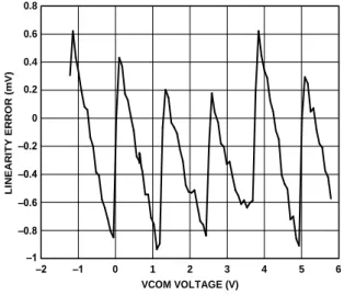
アクティブ負荷
負荷制御情報については表 29 を参照。 表 6.
Parameter Min Typ Max Unit Test
Level Conditions/Comments
DC SPECIFICATIONS Load active on, RCV active, unless otherwise noted
Input Characteristics
VCOM Voltage Range −1.25 +5.75 V D
VDUT Range −1.5 +6.0 V D
VCOM Accuracy, Uncalibrated
−200 ±30 +200 mV P IOH = IOL = 6 mA, VCOM error measured at the calibration points of 0.0 V and 5.0 V
VCOM Resolution 0.6 1 mV PF IOH = IOL = 6 mA, after two-point gain/offset calibration;
range/number of DAC bits as measured at the calibration points of 0.0 V and 5.0 V
VCOM DNL ±1 mV CT IOH = IOL = 6 mA, after two-point gain/offset calibration
VCOM INL −7 ±2 +7 mV P IOH = IOL = 6 mA, after two-point gain/offset calibration; measured over VCOM range of −1.25 V to +5.75 V
DUTGND Voltage Accuracy
−7 ±1 +7 mV P Over ±0.1 V range; measured at end points of VCOM functional range
Output Characteristics IOL
Maximum Source Current 12 mA D
Uncalibrated Offset −600.0 ±100 +600.0 µA P IOH = 0 mA, VCOM = 1.5 V, VDUTx = 0.0 V, IOL offset calculated
from the calibration points of 1 mA and 11 mA
Uncalibrated Gain −12 ±4 +12 % P IOH = 0 mA, VCOM = 1.5 V, VDUTx = 0.0 V, IOL gain calculated
from the calibration points of 1 mA and 11 mA
Resolution 1.5 2 µA PF IOH = 0 mA, VCOM = 1.5 V, VDUTx = 0.0 V, after two-point gain/
offset calibration; range/number of DAC bits as measured at the calibration points of 1 mA and 11 mA
DNL ±3.0 µA CT IOH = 0 mA, VCOM = 1.5 V, VDUTx = 0.0 V, after two-point
gain/offset calibration
INL −80 ±20 +80 µA P IOH = 0 mA, VCOM = 1.5 V, VDUTx = 0.0 V, after two-point gain/
offset calibration; measured over IOL range of 0 mA to 12 mA 90% Commutation Volt
age
0.25 V P IOH = IOL = 12 mA, VCOM = 2.0 V, measure IOL reference at VDUTx = −1.0 V, measure IOL current at VDUTx = 1.75 V, ensure > 90%
of reference current IOH
Maximum Sink Current 12 mA D
Uncalibrated Offset −600.0 ±100 +600.0 µA P IOL = 0 mA, VCOM = 1.5 V, VDUTx = 3.0 V, IOH offset calculated
from the calibration points of 1 mA and 11 mA
Uncalibrated Gain −12 ±4 +12 % P IOL = 0 mA, VCOM = 1.5 V, VDUTx = 3.0 V, IOH gain calculated
from the calibration points of 1 mA and 11 mA
Resolution 1.5 2 µA PF IOL = 0 mA, VCOM = 1.5 V, VDUTx = 3.0 V, after two-point
gain/offset calibration; range/number of DAC bits as measured at the calibration points of 1 mA and 11 mA
DNL ±3.0 µA CT IOL = 0 mA, VCOM = 1.5 V, VDUTx = 3.0 V, after two-point
gain/offset calibration
INL −80 ±20 +80 µA P IOL = 0 mA, VCOM = 1.5 V, VDUTx = 3.0 V, after two-point gain/
offset calibration; measured over IOH range of 0 mA to 12 mA 90% Commutation
Voltage
0.25 V P IOH = IOL =12 mA, VCOM = 2.0 V, measure IOH reference at VDUTx = 5.0 V, measure IOH current at VDUTx = 2.25 V, ensure > 90%
of reference current
Output Current Tempco ±1.5 µA/°
C
Parameter Min Typ Max Unit Test
Level Conditions/Comments
AC SPECIFICATIONS Load active on, unless otherwise noted
Dynamic Performance Propagation Delay, Load
Active On to Load Active Off;
50%, 90%
7.3 ns CB Toggle RCV, DUTx terminated 50 Ω to GND, IOH = IOL = 12 mA,
VH = VL = 0 V, VCOM = +1.25 V for IOL and VCOM = −1.25 V for IOH; measured from 50% point of RCVxP − RCVxN to 90% point of final output, repeat for drive low and high
Propagation Delay, Load Active Off to Load Active On;
50%, 90%
10.3 ns CB Toggle RCV, DUTx terminated 50 Ω to GND, IOH = IOL = 12 mA,
VH = VL = 0 V, VCOM = +1.25 V for IOL and VCOM = −1.25 V for IOH; measured from 50% point of RCVxP − RCVxN to 90% point of final output, repeat for drive low and high
Propagation Delay Matching 3.0 ns CB Toggle RCV, DUTx terminated 50 Ω to GND, IOH = IOL = 12 mA,
VH = VL = 0 V, VCOM = +1.25 V for IOL and VCOM = −1.25 V for IOH; active on vs. active off, repeat for drive low and high Load Spike 190 mV CB Toggle RCV, DUTx terminated 50 Ω to GND, IOH = IOL = 0 mA,
VH = VL = 0 V, VCOM = +1.25 V for IOL and VCOM = −1.25 V for IOH; repeat for drive low and high
Settling Time to 90% 1.9 ns CB Toggle RCV, DUTx terminated 50 Ω to GND, IOH = IOL = 12 mA,
VH = VL = 0 V, VCOM = +1.25 V for IOL and VCOM = −1.25 V for IOH; measured at 90% of final value
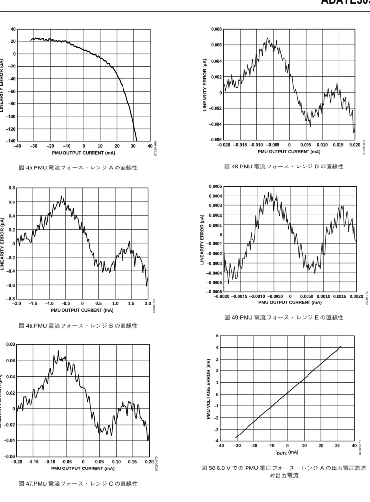
PMU
FV =電圧フォース、MV =電圧測定、FI =電流フォース、MI =電流測定、FN =フォースなし。 表 7.
Parameter Min Typ Max Unit
Test
Level Conditions/Comments
FORCE VOL TAGE (FV)
Current Range A ±32 mA D
Current Range B ±2 mA D
Current Range C ±200 µA D
Current Range D ±20 µA D
Current Range E ±2 µA D
Force Input Voltage Range at Output for All Ranges
−1.5 +6.0 V D
Force Voltage Uncalibrated Accuracy for Range C
−100 ±25 +100 mV P PMU enabled, FV, Range C, PE disabled, error measured at calibration points of 0.0 V and 5.0 V
Force Voltage Uncalibrated Accuracy for All Ranges
±25 mV CT PMU enabled, FV, PE disabled, error measured at calibration
points of 0.0 V and 5.0 V; repeat for each PMU current range Force Voltage Offset Tempco
for All Ranges
±25 µV/°C CT Measured at calibration points for each PMU current range
Force Voltage Gain Tempco for All Ranges
±10 ppm/°C CT Measured at calibration points for each PMU current range
Forced Voltage INL −7 ±2 +7 mV P PMU enabled, FV, Range C, PE disabled, after two-point gain/offset calibration; measured over output range of −1.5 V to +6.0 V Force Voltage Compliance vs.
Current Load
PMU enabled, FV, PE disabled, force −1.5 V, measure voltage while PMU sinking zero and full-scale current; measure ∆V; force 6.0 V, measure voltage while PMU sourcing zero and full-scale current; measure ∆V; repeat for each PMU current range
Range A ±4 mV CT
Parameter Min Typ Max Unit
Test
Level Conditions/Comments
Current Limit, Source, and Sink
Range A 108 140 180 %FS P PMU enabled, FV, PE disabled; sink: force 2.5 V, short DUTx to 6.0 V; source: force 2.5 V, short DUTx to −1.0 V; Range A FS = 32 mA, 108% FS = 35 mA, 180% FS = 58 mA
Range B to Range E 120 145 180 %FS P PMU enabled, FV, PE disabled; sink: force 2.5 V, short DUTx to 6.0 V; source: force 2.5 V, short DUTx to −1.0 V; repeat for each PMU current range; example: Range B FS = 2 mA, 120 % FS = 2.4 mA, 180% FS = 3.6 mA
DUTGND Voltage Accuracy −7 ±1 +7 mV P Over ±0.1 V range; measured at end points of FV functional range
MEASURE CURRENT (MI) VDUTx externally forced to 0.0V, unless otherwise specified,
ideal MEASOUT transfer functions: VMEASOUT01 [V] =
(IMEASOUT01 × 5/FSR) + 2.5 + VDUTGND I(VMEASOUT01) [A] =
(VMEASOUT01 − VDUTGND − 2.5) × FSR/5
Measure Current, Pin DUTx Voltage Range for All Ranges
−1.5 +6.0 V D
Measure Current Uncalibrated Accuracy
Range A ±500 µA CT PMU enabled, FIMI, Range A, PE disabled, error at calibration
points −25 mA and +25 mA, error = (I(VMEASOUT01) − IDUTx)
Range B −400 ±3.0 +400 µA P PMU enabled, FIMI, Range B, PE disabled, error at calibration points −1.6 mA and +1.6 mA, error = (I(VMEASOUT01) − IDUTx)
Range C ± 2.00 µA CT PMU enabled, FIMI, PE disabled, error at calibration points of
±80% FS, error = (I(VMEASOUT01)1 − IDUTx)
Range D ±0.30 µA CT PMU enabled, FIMI, PE disabled, error at calibration points of
±80% FS, error = (I(VMEASOUT01) − IDUTx)
Range E ±0.08 µA CT PMU enabled, FIMI, PE disabled, error at calibration points of
±80% FS, error = (I(VMEASOUT01) − IDUTx)
Measure Current Offset Tempco
Range A ±2 µA/°C CT Measured at calibration points
Range B ±25 nA/°C CT Measured at calibration points
Range C ±5 nA/°C CT Measured at calibration points
Range D and Range E ±1 nA/°C CT Measured at calibration points
Measure Current Gain Error, Nominal Gain = 1
Range A ±2.5 % CT PMU enabled, FIMI, PE disabled, gain error from calibration
points ±80% FS
Range B −20 ±2 +20 % P PMU enabled, FIMI, Range B, PE disabled, gain error from calibration points ±1.6 mA
Range C to Range E ±4 % CT PMU enabled, FIMI, PE disabled, gain error from calibration
points ±80% FS
Measure Current Gain Tempco Measured at calibration points
Range A ±300 ppm/°C CT
Range B to Range E ±50 ppm/°C CT
Measure Current INL
Range A ±0.05 %FSR CT PMU enabled, FIMI, Range A, PE disabled, after two-point
gain/offset calibration, measured over FSR output of −32 mA to +32 mA
Range B −0.02 +0.02 %FSR P PMU enabled, FIM,I Range B, PE disabled, after two-point gain/ offset calibration measured over FSR output of −2 mA to +2 mA Range B to Range E ±0.01 %FSR CT PMU enabled, FIMI, PE disabled, after two-point gain/offset
calibration; measured over FSR output FVMI DUT Pin Voltage
Rejection
−0.01 +0.01 %FSR/ V
P PMU enabled, FVMI, Range B, PE disabled, force −1 V and +5 V into load of 1 mA; measure ∆I reported at MEASOUT01 DUTGND Voltage Accuracy ±2.5 mV CT Over ±0.1 V range; measured at end points of MI functional range
Parameter Min Typ Max Unit
Test
Level Conditions/Comments
FORCE CURRENT (FI) VDUTx externally forced to 0.0V, unless otherwise specified,
ideal force current transfer function: IFORCE = (PMUDAC − 2.5) ×
(FSR/5) Force Current, DUTx Pin
Voltage Range for All Ranges
−1.5 +6.0 V D
Force Current Uncalibrated Accuracy
Range A −5.0 ±0.5 +5.0 mA P PMU enabled, FIMI, Range A, PE disabled, error at calibration points of −25 mA and +25 mA
Range B −400 ±40 +400 µA P PMU enabled, FIMI, Range B, PE disabled, error at calibration points of −1.6 mA and 1.6 mA
Range C −40 ±4 +40 µA P PMU enabled, FIMI, Range C, PE disabled, error at calibration points of ±80% FS
Range D −4 ±0.4 +4 µA P PMU enabled, FIMI, Range D, PE disabled, error at calibration points of ±80% FS
Range E −400 ±75 +400 nA P PMU enabled, FIMI, Range E, PE disabled, error at calibration points of ±80% FS
Force Current Offset Tempco
Range A ±1 µA/°C CT Measured at calibration points
Range B ±80 nA/°C CT Measured at calibration points
Range C to Range E ±4 nA/°C CT Measured at calibration points
Forced Current Gain Error, Nominal Gain = 1
−20 ±4 +20 % P PMU enabled, FIMI, PE disabled, gain error from calibration points of ±80% FS
Forced Current Gain Tempco Measured at calibration points
Range A −500 ppm/°C CT
Range B to Range E ±75 ppm/°C CT
Force Current INL
Range A −0.3 ±0.05 +0.3 %FSR P PMU enabled, FIMI, Range A, PE disabled, after two-point gain/offset calibration; measured over FSR output of −32 mA to +32 mA
Range B to Range E −0.2 ±0.015 +0.2 %FSR P PMU enabled, FIMI, PE disabled, after two-point gain/offset calibration; measured over FSR output
Force Current Compliance vs. Voltage Load
PMU enabled, FIMV, PE disabled; force positive full-scale current driving −1.5 V and +6.0 V, measure ∆I @ DUTx pin; force negative full-scale current driving −1.5 V and +6.0 V, measure ∆I @ DUTx pin
Range A to Range D −0.6 ±0.06 +0.6 %FSR P
Range E −1.0 ±0.1 +1.0 %FSR P
MEASURE VOLTAGE
Measure Voltage Range −1.5 +6.0 V D
Measure Voltage Uncalibrated Accuracy
−25 ±2.0 +25 mV P PMU enabled, FVMV, Range B, PE disabled, error at calibration points 0 V and 5 V, error = (VMEASOUT01 − VDUTx)
Measure Voltage Offset Tempco ±10 µV/°C CT Measured at calibration points
Measure Voltage Gain Error −2 ±0.01 +2 % P PMU enabled, FVMV, Range B, PE disabled, gain error from calibration points 0 V and 5 V
Measure Voltage Gain Tempco 25 ppm/°C CT Measured at calibration points
Measure Voltage INL −7 ±1 +7 mV P PMU enabled, FVMV, Range B, PE disabled, after two-point gain/offset calibration; measured over output range of −1.5 V to +6.0 V
Rejection of Measure V vs. IDUTx −1.5 ±0.1 +1.5 mV P PMU enabled, FVMV, Range D, PE disabled, force 0 V into
load of −10 µA and +10 µA; measure ∆V reported at MEASOUT01
Parameter Min Typ Max Unit
Test
Level Conditions/Comments
MEASOUT01 DC CHARACTERISTICS
MEASOUT01 Voltage Range −1.5 +6.0 V D
DC Output Current 4 mA D
MEASOUT01 Pin Output Impedance
25 200 Ω P PMU enabled, FVMV, PE disabled; source resistance: PMU force 6.0 V and load with 0 mA and 4 mA; sink resistance: PMU force −1.5 V and load with 0 mA and −4 mA; resistance = ∆V/∆I at MEASOUT01 pin
Output Leakage Current when Tristated
−1 +1 µA P Tested at −1.5 V and +6.0 V
Output Short-Circuit Current −25 +25 mA P PMU enabled, FVMV, PE disabled; source: PMU force +6.0 V, short MEASOUT01 to −1.5 V; sink: PMU force −1.5 V, short MEASOUT01 to +6.0 V
VOLTAGE CLAMPS
Low Clamp Range (VCL) −1.5 +4.0 V D
High Clamp Range (VCH) 0.0 6.0 V D
Positive Clamp Voltage Droop −300 +10 +300 mV P PMU enabled, FIMI, Range A, PE disabled, PMU clamps enabled, VCH = 5 V,VCL = −1 V, PMU force 2 mA and 32 mA into open; ∆V seen at DUTx pin
Negative Clamp Voltage Droop −300 −10 +300 mV P PMU enabled, FIMI, Range A, PE disabled, PMU clamps enabled, VCH = 5 V,VCL = −1 V, PMU force −2 mA and −32 mA into open; ∆V seen at DUTx pin
Uncalibrated Accuracy −250 ±100 +250 mV P PMU enabled, FIMI, Range B, PE disabled, PMU clamps enabled, PMU force ±1 mA into open; VCH errors at calibration points 0 V and 5 V; VCL errors at the calibration points 0 V and 4 V INL −70 ±5 +70 mV P PMU enabled, FIMI, Range B, PE disabled, PMU clamps enabled,
PMU force ±1 mA into open; after two-point gain/offset calibration; measured over PMU clamp range
DUTGND Voltage Accuracy ±1 mV CT Over ±0.1 V range; measured at end points of PMU clamp
functional range
SETTLING/SWITCHING TIMES SCAP = 330 pF, FFCAP = 220 pF
Voltage Force Settling Time to 0.1% of Final Value:
PMU enabled, FV, PE disabled, program PMUDAC steps of 500 mV and 5.0 V; simulation of worst case, 2000 pF load, PMUDAC step of 5.0 V Range A, 200 pF and 2000 pF Load 15 µs S Range B, 200 pF and 2000 pF Load 20 µs S Range C, 200 pF and 2000 pF Load 124 µs S Range D, 200 pF and 2000 pF Load 1015 µs S Range E, 200 pF and 2000 pF Load 3455 µs S
Voltage Force Settling Time to 1.0% of Final Value:
PMU enabled, FV, PE disabled, start with PMUDAC programmed to 0.0 V, program PMUDAC to 500 mV Range A, 200 pF and 2000 pF Load 14 µs CB Range B, 200 pF and 2000 pF Load 14 µs CB Range C, 200 pF and 2000 pF Load 14 µs CB Range D, 200 pF Load 45 µs CB Range D, 2000 pF Load 45 µs CB Range E, 200 pF Load 45 µs CB Range E, 2000 pF Load 225 µs CB
Parameter Min Typ Max Unit
Test
Level Conditions/Comments
Voltage Force Settling Time to 1.0% of Final Value:
PMU enabled, FV, PE disabled, start with PMUDAC programmed to 0.0 V, program PMUDAC to 5.0 V Range A, 200 pF and 2000 pF Load 4.0 µs CB Range B, 200 pF Load 4.2 µs CB Range B, 2000 pF Load 4.2 µs CB Range C, 200 pF Load 5.8 µs CB Range C, 2000 pF Load 19 µs CB Range D, 200 pF Load 50 µs CB Range D, 2000 pF Load 210 µs CB Range E, 200 pF Load 360 µs CB Range E, 2000 pF Load 610 µs CB
Current Force Settling Time to 0.1% of Final Value
PMU enabled, FI, PE disabled, start with PMUDAC programmed to 0 current, program PMUDAC to FS current Range A, 200 pF in Parallel with 120 Ω 8.2 µs S Range B, 200 pF in Parallel with 1.5 kΩ 9.4 µs S Range C, 200 pF in Parallel with 15.0 kΩ 30 µs S Range D, 200 pF in Parallel with 150 kΩ 281 µs S Range E, 200 pF in Parallel with 1.5 MΩ 2668 µs S
Current Force Settling Time to 1.0% of Final Value:
PMU enabled, FI, PE disabled, start with PMUDAC programmed to 0 current, program PMUDAC to FS current Range A, 200 pF in Parallel with 120 Ω 4.2 µs CB Range B, 200 pF in Parallel with 1.5 kΩ 4.3 µs CB Range C, 200 pF in Parallel with 15.0 kΩ 8.1 µs CB Range D, 200 pF in Parallel with 150 kΩ 205 µs CB Range E, 200 pF in Parallel with 1.5 MΩ 505 µs CB INTERACTION AND CROSSTALK
Measure Voltage Channel-to-Channel Crosstalk
±0.125 %FSR CT PMU enabled, FIMV, PE disabled, Range B, forcing 0 mA into
0 V load; other channel: Range A, forcing a step of 0 mA to 25 mA into 0 V load; report ∆V of MEASOUT01 pin under test; 0.125% × 8.0 V = 10 mV
Measure Current Channel-to-Channel Crosstalk
±0.01 %FSR CT PMU enabled, FVMI, PE disabled, Range E, forcing 0 V into
0 mA current load; other channel: Range E, forcing a step of 0 V to 5 V into 0 mA current load; report ∆V of MEASOUT01 pin under test; 0.01% × 5.0 V = 0.5 mV
外部検出(PMUS_CHx)
表 8.
Parameter Min Typ Max Unit
Test
Level Conditions/Comments
EXTERNAL SENSE (PMUS_CHX)
Voltage Range −1.5 +6.0 V D
DUTGND 入力
表 9.Parameter Min Typ Max Unit
Test
Level Conditions/Comments
DUTGND INPUT
Input Voltage Range, Referenced to GND −0.1 +0.1 V D
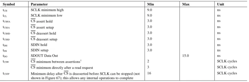
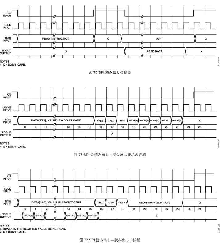
シリアル・ペリフェラル・インターフェース
表 10. Parameter Min Ty p Max Unit Test Level Conditions/Comments SERIAL PERIPHERAL INTERFACESerial Input Logic High 1.8 VCC V PF
Serial Input Logic Low 0 0.7 V PF
Input Bias Current −10 1 +10 μA P Tested at 0.0 V and 3.3 V
SCLK Clock Rate 50 MHz PF
SCLK Pulse Width 9 ns CT
SCLK Crosstalk on DUT x Pin
8 mV CB PE disabled, PMU FV enabled and forcing 0 V
Serial Output Logic High VCC − 0.
4
VCC V PF Sourcing 2 mA
Serial Output Logic Low 0 0.8 V PF Sinking 2 mA
Update Time 10 μs D Maximum delay time required for the part to enter a stable state after a serial bus command is loaded
HVOUT ドライバ
表 11.Parameter Min Typ Max Unit
Test
Level Conditions/Comments
VHH BUFFER VHH = (VT + 1 V) × 2 + DUTGND
Voltage Range 5.9 VPLUS − 3.
25
V D VPLUS = 16.75 V nominal; in this condition, VHVOUT max =
13.5 V
Output High 13.5 V P VHH mode enabled, RCV active, VHH level = full scale,
sourcing 15 mA
Output Low 5.9 V P VHH mode enabled, RCV active, VHH level = zero scale,
sinking 15 mA
Accuracy Uncalibrated −500 ±100 +500 mV P VHH mode enabled, RCV active, VHVOUT error measured at
the calibration points of 7 V and 12 V
Offset Tempco 1 mV/°C CT Measured at calibration points
Resolution 1.21 1.5 mV PF VHH mode enabled, RCV active, after two-point gain/offset
calibration; range/number of DAC bits as measured at the calibration points of 7 V and 12 V
INL −30 ±15 +30 mV P VHH mode enabled, RCV active, after two-point gain/offset calibration; measured over VHH range of 5.9 V to 13.5 V DUTGND Voltage Accuracy ±1 mV CT Over ±0.1 V range; measured at end points of VHH
functional range
Output Resistance 1 10 Ω P VHH mode enabled, RCV active, source: VHH = 10.0 V, IHVOUT= 0 mA and 15 mA; sink: VHH = 6.5 V, IHVOUT = 0
mA and −15 mA; ∆V/∆I DC Output Current Limit
Source
60 100 mA P VHH mode enabled, RCV active, VHH = 10.0 V, short HVOUT pin to 5.9 V, measure current
DC Output Current Limit Sink −100 −60 mA P VHH mode enabled, RCV active, VHH = 6.5 V, short HVOUT pin to 14.1 V, measure current
Rise Time (From VL or VH to VHH)
200 ns CB VHH mode enabled, toggle RCV, VHH = 13.5 V, VL = VH
= 3.0 V; 20% to 80%, for DATA = high and DATA = low Fall Time (From VHH to VL
or VH)
26 ns CB VHH mode enabled, toggle RCV, VHH = 13.5 V, VL = VH
= 3.0 V; 20% to 80%, for DATA = high and DATA = low Preshoot, Overshoot, and
Undershoot
±125 mV CB VHH mode enabled, toggle RCV, VHH = 13.5 V, VL = VH
Parameter Min Typ Max Unit
Test
Level Conditions/Comments
VL/VH BUFFER
Voltage Range −0.1 +6.0 V D
Accuracy Uncalibrated −500 ±100 +500 mV P VHH mode enabled, RCV inactive, error measured at the calibration points 0 V and 5 V
Offset Tempco 1 mV/°C CT Measured at calibration points
Resolution 0.61 0.75 mV PF VHH mode enabled, RCV inactive, after two-point
gain/offset calibration; range/number of DAC bits as measured at the calibration points 0 V and 5 V
INL −20 ±4 +20 mV P VHH mode enabled, RCV inactive, after two-point
gain/offset calibration; measured over range of −0.1 V to +6.0 V
DUTGND Voltage Accuracy ±2 mV CT Over ±0.1 V range; measured at end points of VH and VL,
functional range
Output Resistance 46 48 50 Ω P VHH mode enabled, RCV inactive, source: VH = 3.0 V, IHVOUT = 1 mA and 50 mA; sink: VL = 2.0 V, IHVOUT = −1
mA and −50 mA; ∆V/∆I DC Output Current Limit
Source
60 100 mA P VHH mode enabled, RCV inactive, VH = 6.0 V, short HVOUT pin to −0.1 V, DATA high, measure current DC Output Current Limit Sink −100 −60 mA P VHH mode enabled, RCV inactive, VL = −0.1 V, short
HVOUT pin to 6.0 V, DATA low, measure current
Rise Time (VL to VH) 10.0 ns CB VHH mode enabled, RCV inactive, VL = 0.0 V, VH = 3.0 V,
toggle DATA; 20% to 80%
Fall Time (VH to VL) 11.3 ns CB VHH mode enabled, RCV inactive, VL = 0.0 V, VH = 3.0 V,
toggle DATA; 20% to 80% Preshoot, Overshoot, and
Undershoot
±54 mV CB VHH mode enabled, RCV inactive, VL = 0.0 V, VH = 3.0 V,
toggle DATA
過電圧検出器(OVD)
表 12.
Parameter Min Typ Max Unit
Test
Level Conditions/Comments
DC CHARACTERISTICS
Programmable Voltage Range −3.0 +7.0 V D
Accuracy Uncalibrated −200 +200 mV P OVD offset errors measured at programmed levels of +7.0 V and −3.0 V
Hysteresis 112 mV CB
LOGIC OUTPUT CHARACTERISTICS
Off State Leakage 10 1000 nA P Disable OVD alarm, apply 3.3 V to OVD pin, measure leakage current
Max On Voltage @ 100 μA 0.2 0.7 V P Activate alarm, force 100 μA into OVD pin, measure active alarm voltage
Propagation Delay 1.6 μs CB For OVD high: DUTx = 0 V to 6 V swing, OVD high = 3.0 V,
OVD low = −3.0 V; for OVD low: DUTx = 0 V to 6 V swing, OVD high = 7.0 V, OVD low = 3.0 V
16 ビット DAC モニター・マルチプレクサ
表 13.Parameter Min Typ Max Unit
Test
Level Conditions/Comments
DC CHARACTERISTICS
Programmable Voltage Range −2.5 +7.5 V D
絶対最大定格
表 14.
Parameter Rating
Supply Voltages
Positive Supply Voltage (VDD to GND) −0.5 V to +11.0 V
Positive VCC Supply Voltage (VCC to GND) −0.5 V to +4.0 V
Negative Supply Voltage (VSS to GND) −6.25 V to +0.5 V
Supply Voltage Difference (VDD to VSS) −1.0 V to +16.5 V
Reference Ground (DUTGND to GND) −0.5 V to +0.5 V
AGND to DGND −0.5 V to +0.5 V
VPLUS Supply Voltage (VPLUS to GND) −0.5 V to +17.5 V
Input Voltages
Input Common-Mode Voltage VSS to VDD
Short-Circuit Voltage1 −3.0 V to +8.0 V
High Speed Input Voltage2 0.0 V to VCC
High Speed Differential Input Voltage3 0.0 V to V CC
VREF −0.5 V to +5.5 V
DUTx I/O Pin Current
DCL Maximum Short-Circuit Current4 ±140 mA
Temperature
Operating Temperature, Junction 125°C
Storage Temperature Range −65°C to +150°C
1 RL = 0 Ω、VDUT連続短絡条件、(VH、VL、VT、高 Z、VCOM、クラン プ・モード)。 2ソース R = 0 Ω での DATAxP、DATAxN、RCVxP、RCVxN。 3 DATAxP~DATAxN、RCVxP、RCVxN。 4 RL = 0 Ω、VDUTx = –3 V~+8 V、DCL 電流制限。連続短絡条件。 ADATE305 は電流を制限して、連続短絡に耐える必要があります。 上記の絶対最大定格を超えるストレスを加えるとデバイスに恒 久的な損傷を与えることがあります。この規定はストレス定格 の規定のみを目的とするものであり、この仕様の動作の節に記 載する規定値以上でのデバイス動作を定めたものではありませ ん。デバイスを長時間絶対最大定格状態に置くとデバイスの信 頼性に影響を与えます。
熱抵抗
冷却液仕様の場合、θJC = 1.1°C/W。 表 15.熱抵抗 Airflow θJA Unit Natural Convection 33 °C/W1 meter per second 30 °C/W
2 meters per second 28.5 °C/W
テスト・レベルの説明
D 定義 S デザインの評価シミュレーションを実施。 P 100%の出荷テストを実施。 PF 出荷テストで機能を確認。 CT テスタ上でキャラクタライゼーションを実施。 CB ベンチでキャラクタライゼーションを実施。ESD の注意
ESD(静電放電)の影響を受けやすいデバイスで す。電荷を帯びたデバイスや回路ボードは、検知 されないまま放電することがあります。本製品は 当社独自の特許技術である ESD 保護回路を内蔵 してはいますが、デバイスが高エネルギーの静電 放電を被った場合、損傷を生じる可能性がありま す。したがって、性能劣化や機能低下を防止する ため、ESD に対する適切な予防措置を講じるこ とをお勧めします。ピン配置およびピン機能説明
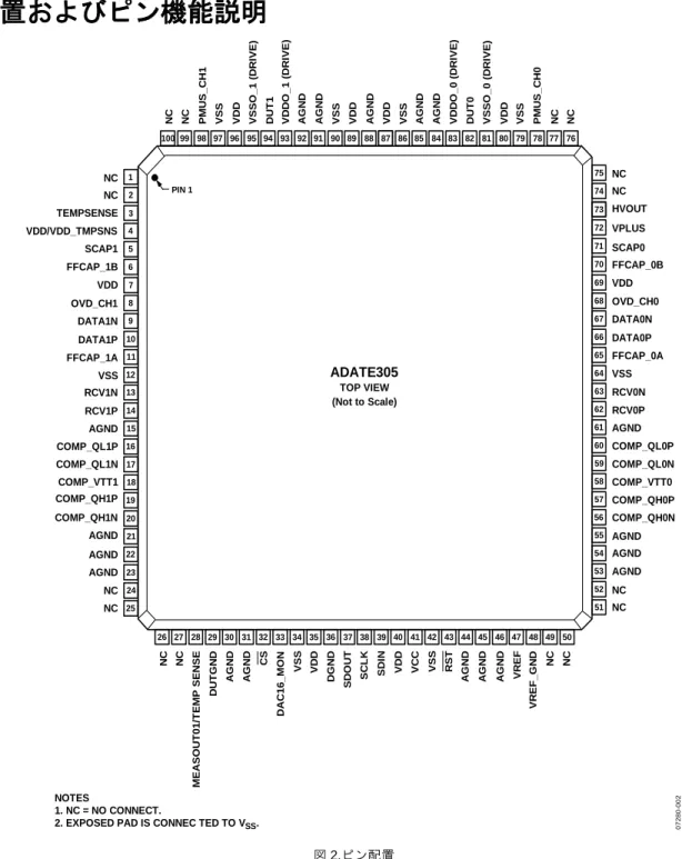
PIN 1 ADATE305 TOP VIEW (Not to Scale) 1 2 3 4 5 6 7 8 9 10 11 12 13 14 15 16 17 18 19 20 21 22 23 24 25 26 27 28 29 30 31 32 33 34 35 36 37 38 39 40 41 42 43 44 45 46 47 48 49 50 76 77 78 79 80 81 82 83 84 85 86 87 88 89 90 91 92 93 94 95 96 97 98 99 100 51 52 53 54 55 56 57 58 59 60 61 62 63 64 65 66 67 68 69 70 71 72 73 74 75 0 7 2 8 0 -0 0 2 NC NC AGND AGND AGND COMP_QH1N COMP_QH1P COMP_VTT1 COMP_QL1N COMP_QL1P AGND RCV1P RCV1N VSS FFCAP_1A DATA1P DATA1N OVD_CH1 VDD FFCAP_1B SCAP1 VDD/VDD_TMPSNS TEMPSENSE NC NC NC NC AGND AGND AGND COMP_QH0N COMP_QH0P COMP_VTT0 COMP_QL0N COMP_QL0P AGND RCV0P RCV0N VSS FFCAP_0A DATA0P DATA0N OVD_CH0 VDD FFCAP_0B SCAP0 VPLUS HVOUT NC NC NC NC PM U S_ C H 0 VSS VD D VS SO _ 0 (D R IVE ) D U T 0 VD D O _ 0 (D R IVE ) A G N D A G N D VSS VD D A G N D VD D VSS A G N D A G N D VD D O _ 1 (D R IVE) D U T 1 VSSO _ 1 (D R IVE) VD D VSS PM U S_ C H 1 NC NC NC NC VR EF _ G N D VR EF A G N D A G N D A G N D R ST VSS VC C VD D S D IN S C L K SD O U T D G N D VD D VSS D A C 1 6 _ M O N CS A G N D A G N D D U T G N D ME A SO U T 0 1 /T EM P SE N SE NC NC NOTES 1. NC = NO CONNECT.2. EXPOSED PAD IS CONNEC TED TO VSS.
図 2.ピン配置 表 16.ピン機能の説明 ピン番号 記号 説明 1 NC 未接続。チップへの接続なし。 2 NC 未接続。チップへの接続なし。 3 TEMPSENSE 温度検出出力。 4 VDD/VDD_TMPSNS 温度検出電源+10.0 V。 5 SCAP1 PMU 安定化コンデンサ接続チャンネル 1 (330 pF)。 6 FFCAP_1B PMU フィードフォワード・コンデンサ接続 B チャンネル 1 (220 pF)。 7 VDD 電源+10.0 V。 8 OVD_CH1 過電圧検出フラグ出力チャンネル 1。
ピン番号 記号 説明 11 FFCAP_1A PMU フィードフォワード・コンデンサ接続 A チャンネル 1 (220 pF)。 12 VSS 電源−5.75 V。 13 RCV1N 受信データ入力(負)チャンネル 1。 14 RCV1P 受信データ入力(正)チャンネル 1。 15 AGND アナログ・グラウンド。 16 COMP_QL1P ローサイド・コンパレータ出力(正)チャンネル 1。 17 COMP_QL1N ローサイド・コンパレータ出力(負)チャンネル 1。 18 COMP_VTT1 コンパレータ電源チャンネル 1。 19 COMP_QH1P ハイサイド・コンパレータ出力(正)チャンネル 1。 20 COMP_QH1N ハイサイド・コンパレータ出力(負)チャンネル 1。 21 AGND アナログ・グラウンド。 22 AGND アナログ・グラウンド。 23 AGND アナログ・グラウンド。 24 NC 未接続。チップへの接続なし。 25 NC 未接続。チップへの接続なし。 26 NC 未接続。チップへの接続なし。 27 NC 未接続。チップへの接続なし。
28 MEASOUT01/TEMP SENSE 共用ピン。PMU MEASOUT チャンネル 0、PMU MEASOUT チャンネル 1、温度検出/
温度検出 GND リファレンス間で共用。 29 DUTGND 被テスト・デバイスのグラウンド基準。 30 AGND アナログ・グラウンド。 31 AGND アナログ・グラウンド。 32 CS シリアル・ペリフェラル・インターフェース(SPI®)のチップ・セレクト。 33 DAC16_MON 16 ビット DAC モニター・マルチプレクサ出力。 34 VSS 電源−5.75 V。 35 VDD 電源+10.0 V。 36 DGND デジタル・グラウンド。 37 SDOUT シリアル・プログラマブル・インターフェース(SPI)のデータ出力。 38 SCLK シリアル・プログラマブル・インターフェース(SPI)のクロック。 39 SDIN シリアル・プログラマブル・インターフェース(SPI)のデータ入力。 40 VDD 電源+10.0 V。 41 VCC 電源+3.3 V。 42 VSS 電源−5.75 V。 43 RST シリアル・ペリフェラル・インターフェース(SPI)のリセット。 44 AGND アナログ・グラウンド。 45 AGND アナログ・グラウンド。 46 AGND アナログ・グラウンド。 47 VREF +5 V DAC リファレンス電圧。 48 VREF_GND DAC グラウンド基準。 49 NC 未接続。チップへの接続なし。 50 NC 未接続。チップへの接続なし。 51 NC 未接続。チップへの接続なし。 52 NC 未接続。チップへの接続なし。 53 AGND アナログ・グラウンド。 54 AGND アナログ・グラウンド。 55 AGND アナログ・グラウンド。 56 Comp_QH0N ハイサイド・コンパレータ出力(負)チャンネル 0。 57 Comp_QH0P ハイサイド・コンパレータ出力(正)チャンネル 0。 58 Comp_VTT0 コンパレータ電源チャンネル 0。 59 Comp_QL0N ローサイド・コンパレータ出力(負)チャンネル 0。 60 Comp_QL0P ローサイド・コンパレータ出力(正)チャンネル 0。 61 AGND アナログ・グラウンド。
ピン番号 記号 説明 62 RCV0P 受信データ入力(正)チャンネル 0。 63 RCV0N 受信データ入力(負)チャンネル 0。 64 VSS 電源−5.75 V。 65 FFCAP_0A PMU フィードフォワード・コンデンサ接続 A チャンネル 0 (220 pF)。 66 DATA0P ドライバ・データ入力(正)チャンネル 0。 67 DATA0N ドライバ・データ入力(負)チャンネル 0。 68 OVD_CH0 過電圧検出フラグ出力チャンネル 0。 69 VDD 電源+10.0 V。 70 FFCAP_0B PMU フィードフォワード・コンデンサ接続 B チャンネル 0 (220 pF)。 71 SCAP0 PMU 安定化コンデンサ接続チャンネル 0 (330 pF)。 72 VPLUS 電源+16.75 V。 73 HVOUT 高電圧ドライバ出力。 74 NC 未接続。チップへの接続なし。 75 NC 未接続。チップへの接続なし。 76 NC 未接続。チップへの接続なし。 77 NC 未接続。チップへの接続なし。 78 PMUS_CH0 PMU 外部検出パス・チャンネル 0。 79 VSS 電源−5.75 V。 80 VDD 電源+10.0 V。 81 VSSO_0 (DRIVE) ドライバ出力電源−5.75 V チャンネル 0。 82 DUT0 被テスト・デバイス・チャンネル 0。 83 VDDO_0 (DRIVE) ドライバ出力電源+10.0 V チャンネル 0。 84 AGND アナログ・グラウンド。 85 AGND アナログ・グラウンド。 86 VSS 電源−5.75 V。 87 VDD 電源+10.0 V。 88 AGND アナログ・グラウンド。 89 VDD 電源+10.0 V。 90 VSS 電源−5.75 V。 91 AGND アナログ・グラウンド。 92 AGND アナログ・グラウンド。 93 VDDO_1 (DRIVE) ドライバ出力電源+10.0 V チャンネル 1。 94 DUT1 被テスト・デバイス・チャンネル 1。 95 VSSO_1 (DRIVE) ドライバ出力電源−5.75 V チャンネル 1。 96 VDD 電源+10.0 V。 97 VSS 電源−5.75 V。 98 PMUS_CH1 PMU 外部検出パス・チャンネル 1。 99 NC 未接続。チップへの接続なし。 100 NC 未接続。チップへの接続なし。 EP 露出パッド。パドルは VSSに接続する必要があります。
代表的な性能特性
0.30 0.25 0.20 0.15 0.10 0.05 0 –0.05 0 2 4 6 8 10 12 14 16 18 TIME (ns) VO L T A G E (V ) 0 7 2 8 0 -0 2 3 0.2V 0.5V 図 3.ドライバ小信号応答; VH = 0.2 V、0.5 V; VL = 0.0 V; 50 Ω 終端 1.6 1.4 1.2 1.0 0.8 0.6 0.4 0.2 0 –0.2 VO L T A G E (V) 0 2 4 6 8 10 12 14 16 18 TIME (ns) 07 2 8 0 -0 2 4 1V 2V 3V 図 4.ドライバ大信号応答; VH = 1.0 V、2.0 V、3.0 V; VL = 0.0 V; 50 Ω 終端 6 5 4 3 2 1 0 –1 VO L T A G E (V ) 0 2 4 6 8 10 12 14 16 18 TIME (ns) 072 8 0 -0 3 1 1V 5V 3V 図 5.ドライバ大信号応答; VH = 1.0 V、3.0 V、5.0 V; VL = 0 .0 V; 500 Ω 終端 1.6 1.4 1.2 1.0 0.8 0.6 0.4 0.2 0 –0.2 4.5 4.0 3.5 2.5 3.0 2.0 1.5 1.0 0.5 0 TIME (ns) VO L T A G E (V) 0 7 2 8 0 -0 2 2 1V 2V 3V 図 6.50 MHz ドライバ応答; VH = 1.0 V、2.0 V、3.0 V; VL = 0.0 V、 50 Ω 終端 1.8 1.6 1.4 1.2 1.0 0.8 0.6 0.4 0.2 0 –0.2 19 0 2 3 4 5 6 7 8 9 10 11 12 13 14 15 16 17 18 TIME (ns) VO L T A G E (V ) 0 7 2 8 0 -0 2 1 1V 2V 3V 図 7.100 MHz ドライバ応答; VH = 1.0 V、2.0 V、3.0 V; VL = 0.0 V; 50 Ω 終端 1.6 1.4 1.2 1.0 0.8 0.6 0.4 0.2 0 0 1 2 3 4 5 6 7 8 9 10 TIME (ns) VO L T A G E (V ) 0 7 2 8 0 -0 3 2 1V 2V 3V 図 8.200 MH での応答; VH = 1.0 V、2.0 V、3.0 V; VL = 0.0 V; 50 Ω 終端1.6 1.4 1.2 1.0 0.8 0.6 0.4 0.2 0 0 0.5 1.0 1.5 2.0 2.5 3.0 3.5 4.0 4.5 5.0 5.5 6.0 6.5 TIME (ns) VO L T A G E (V ) 0 7 2 8 0 -0 2 6 1V 2V 3V 0.5V 図 9.300 MHz ドライバ応答; VH = 0.5 V、1.0 V、2.0 V、3.0 V; VL = 0.0 V; 50 Ω 終端 0.9 0.8 0.7 0.6 0.5 0.4 0.3 0.2 0.1 0 0 0.5 1.0 1.5 2.0 2.5 3.0 3.5 4.0 4.5 TIME (ns) VO L T A G E (V) 0 7 2 8 0 -0 2 7 1V 2V 3V 0.5V 図 10.400 MHz ドライバ応答; VH = 0.5 V、1.0 V、2.0 V、3.0 V; VL = 0.0 V; 50 Ω 終端 1.2 1.0 0.8 0.6 0.4 0.2 0 200 250 300 350 400 450 500 550 600 FREQUENCY (MHz) VO L T A G E (V) 0 7 2 8 0 -0 8 4 図 11.ドライバ・トグル・レート、VH = 2.0 V、VL = 0.0 V、 50 Ω 終端 0.6 0.5 0.4 0.3 0.2 0.1 0 VO L T A G E (V) 0 7 2 8 0 -0 2 8 TIME (ns) 18 16 14 12 10 8 6 4 2 3 5 7 9 11 13 15 17 19 1 0 図 12.VTERM の変化に対するドライバ・アクティブ (VH および VL); VH = 1.0 V、VT = 0.5 V、VL = 0.0 V 1.2 1.0 0.8 0.6 0.4 0.2 0 VO L T A G E (V) TIME (ns) 072 8 0 -0 2 9 18 16 14 12 10 8 6 4 2 3 5 7 9 11 13 15 17 19 1 0 図 13.VTERM の変化に対するドライバ・アクティブ (VH および VL); VH = 2.0 V、VT = 1.0 V、VL = 0.0 V 1.6 1.4 1.2 1.0 0.8 0.6 0.4 0.2 0 –0.2 VO L T A G E (V) 0 TIME (ns) 07 2 8 0 -0 3 0 20 18 16 14 12 10 8 6 4 2 図 14.VTERM の変化に対するドライバ・アクティブ
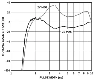
–20 –40 –60 –80 0 20 1 2 3 4 5 6 7 8 9 10 PULSEWIDTH (ns) T R A IL IN G ED G E ER R O R (p s ) 0 7 2 8 0 -0 3 6 0.2V NEG 0.2V POS 図 15.ドライバの最小パルス幅; VH = 0.2 V、VL = 0.0 V –20 –40 –60 0 20 1 2 3 4 5 6 7 8 9 10 PULSEWIDTH (ns) T R A IL IN G ED G E ER R O R (p s ) 0 7 2 8 0 -0 3 7 0.5V NEG 0.5V POS 図 16.ドライバの最小パルス幅; VH = 0.5 V、VL = 0.0 V 0 –10 –20 –30 –40 –50 –60 10 1 2 3 4 5 6 7 8 9 10 PULSEWIDTH (ns) T R A IL IN G ED G E ER R O R (p s ) 0 7 2 8 0 -0 3 3 1V NEG 1V POS 図 17.ドライバの最小パルス幅; VH = 1.0 V、VL = 0.0 V 0 –20 –40 –60 –80 –100 40 20 1 2 3 4 5 6 7 8 9 10 PULSEWIDTH (ns) T R A IL IN G ED G E ER R O R (p s ) 0 7 2 8 0 -0 3 4 2V NEG 2V POS 図 18.ドライバの最小パルス幅; VH = 2.0 V、VL = 0.0 V –20 –40 –60 –80 –100 40 20 0 1 2 3 4 5 6 7 8 9 10 PULSE WIDTH (ns) T R A IL IN G ED G E ER R O R (p s ) 0 7 2 8 0 -0 3 5 3V NEG 3V POS 図 19.ドライバの最小パルス幅; VH = 3.0 V、VL = 0.0 V 1.5 1.0 0.5 0 –0.5 –1.0 –1.5 –2.0 –2 –1 0 1 2 3 4 5 6 7 DRIVER OUTPUT VOLTAGE (V)
L IN EA R IT Y ER R O R (m V) 0 7 2 8 0 -0 5 1 図 20.ドライバ VH の直線性誤差
1.5 1.0 0.5 0 –1.0 –0.5 –1.5 –2 –1 0 1 2 3 4 5 6 DRIVER OUTPUT VOLTAGE (V)
L IN EA R IT Y ER R O R (m V) 0 7 2 8 0 -0 5 2 図 21.ドライバ VL の直線性誤差 1.5 1.0 0.5 0 –0.5 –1.0 –1.5 –2.0 –2 –1 0 1 2 3 4 5 6 DRIVER OUTPUT VOLTAGE (V)
L IN EA R IT Y ER R O R (m V) 0 7 2 8 0 -0 5 3 図 22.ドライバ VT の直線性誤差 48.5 48.0 47.5 47.0 46.5 46.0 –60 –40 –20 0 20 40 60 DRIVER OUTPUT CURRENT (mA)
D R IVER O U T PU T R ESI ST A N C E (Ω ) 0 0 7 2 8 0 -0 5 4 図 23.ドライバ出力抵抗対出力電流 100 90 80 70 50 60 40 30 20 0 10 –10 –2 –1 0 1 2 3 4 5 6 VDUTx (V) D R IVER O U T PU T C U R R EN T (m A ) 0 7 2 8 0 -0 5 5 図 24.ドライバ出力電流制限値;ドライバを−2.0 V に設定; VDUTxを−2.0 V~+6.0 V で掃引 0 –10 –20 –30 –50 –40 –60 –70 –80 –100 –90 –2 –1 0 1 2 3 4 5 6 VDUTx (V) D R IVER O U T PU T C U R R EN T (m A ) 0 7 2 8 0 -0 5 6 図 25.ドライバ出力電流制限値;ドライバを 6.0 V に設定; VDUTxを−2.0 V~+6.0 V で掃引 –722 –723 –724 –725 –726 –727 –728 –729 –730 –1 0 1 2 3 4 5 6 VL PROGRAMMED VOLTAGE (V) L IN EA R IT Y ER R O R (m V) 0 7 2 8 0 -0 5 7 図 26.HVOUT VL の直線性誤差