INVITED PAPER
Special Section on Recent Advances in Integrated Photonic DevicesWavelength Tunable Laser with Silica-Waveguide Ring Resonators
Takeshi TAKEUCHI†a), Morio TAKAHASHI†, Kouichi SUZUKI††, Members, Shinya WATANABE††, Nonmember, and Hiroyuki YAMAZAKI†, Member
SUMMARY We have proposed a tunable laser with silica-waveguide ring resonators. In this tunable laser, a semiconductor optical amplifier was passively aligned and mounted onto a silica-waveguide substrate. The ring resonators can be tuned by controlling their temperatures using the thermo optic heaters formed on them, and there are no mechanically moving parts. Thus, they are sufficiently stable and reliable for practical use. Our tunable laser exhibits a high fiber-output power of more than 15 dBm and a wide tunable range of 60 nm (L-band, 50 GHz spacing, 147 channels). Moreover, a tunable laser with a much wider tunable range of 96 nm using 100-GHz-FSR ring resonators is also reported.
key words: tunable laser, photonic integrated circuit, silica-waveguide, ring resonator
1. Introduction
Wavelength tunable lasers have become key devices in op-tical network systems, such as wavelength division multi-plexing (WDM) and reconfigurable optical add/drop multi-plexing (ROADM) systems, where wavelength plays an im-portant role. Using tunable lasers instead of conventional fixed wavelength lasers will significantly reduce the inven-tory cost for the light source. More over, tunable lasers make the optical network much more efficient and flexible. Sev-eral different device types have been proposed as tunable lasers; monolithic type lasers including a DFB-array type [1] and DBR type [2], [3], and external cavity lasers [4], [5]. In a monolithic type tunable laser, all fundamental functions are integrated on one chip. This makes the size of the tun-able laser very compact, which is an advantage of a mono-lithic type laser. On the other hand, an external cavity laser is composed of a gain section and a tunable filter section. As a gain section, a semiconductor optical amplifier (SOA) is used in most of the cases. Device structure of an SOA chip is generally very simple and does not require compli-cated monolithic integration technology. This simplicity is an advantage of an external cavity laser.
The tunable laser we propose is also classified as an external cavity laser, composed of silica-waveguide ring res-onators as a tunable filter section and a semiconductor opti-cal amplifier (SOA) as a gain section [6]–[11]. The
silica-Manuscript received June 2, 2008. Manuscript revised October 16, 2008.
†The authors are with the Nano Electronics Research
Labora-tories, NEC Corp., Tsukuba-shi, 305-8501 Japan.
††The authors are with the Fiber Optic Device Division, NEC
Corp., Otsuki-shi, 401-0016 Japan. a) E-mail: [email protected]
DOI: 10.1587/transele.E92.C.198
waveguide ring resonators and the SOA were automatically aligned and directly coupled using passive alignment tech-nology [9]; thus, no complicated assembly procedures are required. The ring resonators can be tuned by controlling their temperatures using the thermo optic heaters formed on them, and there are no mechanically moving parts. Thus, they are sufficiently stable and reliable for practical use. Our fabricated tunable laser has exhibited a highly uniform high fiber output power of more than 15 dBm and a wide tunable range of 60 nm covering the full L-band. Also, a tunable laser with an enlarged tunable range up to 96 nm using 100-GHz-FSR ring resonators has been demonstrated.
2. Structure, Design, and Fabrication 2.1 Device Structure
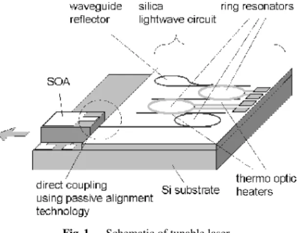
The proposed tunable laser structure is schematically shown in Fig. 1. The tunable laser consists of a silica lightwave cir-cuit and an SOA. As shown in Fig. 2, the SOA was mounted on the Si substrate of the silica lightwave circuit. The SOA and the lightwave circuit were directly butt-coupled using passive alignment technology, which will be described in detail in Sect. 2.4. The SOA was composed of a 1000-μm long gain section and a 280-μm long phase control section with a 220-μm long separation region between them. They had InP-based buried hetero structure waveguides with dif-ferent compositional wavelength, and they were butt-jointed using regrowth technology. The phase control section is used to optimize the optical phase automatically by
so-Fig. 1 Schematic of tunable laser.
Fig. 2 Detailed structures around SOA.
called dither control system. In the dither control system, the phase current is modulated at a small amplitude. By monitoring the tapped optical output power, the DC compo-nent of the phase current is controlled so that the amplitude of the optical output power fluctuation caused by the mod-ulation becomes smallest. Thus, the phase current is opti-mized to give the maximum optical output power. For this purpose, phase control section integrated in the SOA chip is suitable because of its sufficient response speed, while silica-waveguide based phase control section would be in-sufficient for 20-kHz modulation in our dither control sys-tem. The phase current modulation broaden the line width of the laser output, however, to suppress the stimulated Brillouin scattering, the adequately broadened line width is rather desirable. The lightwave circuit consists of three ring resonators which work as tunable filters by using the thermo optic heaters formed on the ring resonators. A waveguide reflector is also employed in the lightwave circuit as an ex-ternal cavity mirror. Nitride-doped-silica (SiON) was used as the core material of the waveguides. The core was 2-μm wide and 1.4-2-μm thick, and it was embedded with silica. The refractive index contrast was 6%, which is large enough to suppress the excess loss at the bend waveguides of the lightwave circuit. Spot-size-converters were introduced in both the SOA and the lightwave circuit at the butt-coupling interface to enlarge the spot sizes on both sides and, conse-quently, to enlarge the coupling tolerance. The size of the tunable laser chip including both the SOA and the lightwave circuit was 6.5 mm long and 4.5 mm wide.
2.2 Wavelength Tuning Using Triple-Ring Resonators Figure 3 shows the configuration of the silica lightwave cir-cuit, and Fig. 4 shows the principle of wavelength tuning using the ring resonators. Three ring resonators, rings 1, 2, and 3, are cascaded in the lightwave circuit. Ring 1 has a free spectral range (FSR) of 50 GHz, which corresponds to the ITU-T grid spacing, and works as a wavelength ref-erence ring. For the precise wavelength adjustment to the
Fig. 3 Configuration of silica lightwave circuit.
Fig. 4 Principle of wavelength tuning using three ring resonators.
ITU-T grid, the temperature of the ring 1 is controlled by the thermo optic heater. The FSRs of rings 2 and 3 (FSR 2, and FSR, respectively) are slightly larger than 50 GHz (50 GHz < FSR 2 < FSR 3), as shown in Fig. 4. The total trans-mittance of the three rings, also shown in Fig. 4, has a maxi-mum value at the wavelength ofλL, where all the three rings have the maximum peak transmittance. The lasing occurs at this wavelengthλL. We can select the lasing wavelength among the ITU-T channels by tuning the peak-transmittance wavelength of rings 2 and 3, which can be controlled with the thermo optic heaters. Although the tuning range of the peak-transmittance wavelength of each ring is not large enough, approximately 0.4 nm for the 200-mW power in-put to the thermo optic heater, the Verneir effect magnifies the tuning range of the lasing wavelength. The tuning range magnification factor M is determined by the equation M=
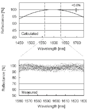
Fig. 5 Calculated and measured reflectance of waveguide reflector.
FSR 2/(FSR 2 − FSR 1), which means a smaller (FSR 2 − FSR 1) value gives a larger M. However, there is a design trade off, namely, a smaller (FSR 2 − FSR 1) value gives a smaller transmittance difference (threshold gain difference) between different channels (Fig. 4), and causes instability in lasing operations. The reason we have introduced the ring structure is to relax this design trade off. The triple-ring structure gives a larger threshold gain difference com-pared with the double-ring structure which was previously reported [6], and provides a more stable lasing over a larger wavelength range.
2.3 Waveguide Reflector
As shown in Fig. 3, the waveguide reflector is a simple struc-ture composed with a 3-dB directional coupler and a loop waveguide, which can be fabricated at the same process as the ring resonators. Thus, the fabrication cost is reduced us-ing a waveguide reflector instead of a high reflection (HR) mirror used in previous works. Figure 5 shows calculated and measured reflectance of the waveguide reflector. A very flat and high reflectance of more than 95% has been con-firmed over the L-band, which is in good agreement with the calculation. Here, the broadening of the measured re-flectance value is due to Fabry-Perot interference caused by undesirable reflections inside the measurement system. 2.4 Passive Alignment Technology
As briefly described in Sect. 2.1, the SOA and the lightwave circuit were directly coupled using passive alignment tech-nology [12], [13]. As shown in Fig. 2, a SOA-mounting area was formed on the silicon substrate of the lightwave circuit, where silica pedestals, alignment marks and electrodes were formed. The SOA chip was mounted with the junction-side
Fig. 6 Horizontal misalignment between SOA and lightwave circuit.
down. The vertical position of the SOA chip was precisely adjusted by the thickness of the silica pedestals. The vertical misalignment was less than 0.2μm, which was determined by the controllability of the silica-deposition thickness. Hor-izontal alignment was performed using the alignment marks, which were also formed on the SOA chip and can be ob-served with infrared light. Figure 6 shows a histogram of the horizontal misalignment between the SOA chip and the lightwave circuit. The average misalignment was 0.044μm, and the standard deviation was 0.21μm. The displacement of the SOA during the soldering process was successfully suppressed by optimizing the soldering conditions such as the thickness of the solder film and soldering temperature profiles. These values of vertical and horizontal misalign-ment are sufficiently small compared with coupling toler-ance between the SOA and the silica waveguide. The 1-dB-down coupling tolerances (full width) were approximately 2μm and 3 μm for vertical and horizontal direction, respec-tively. The average coupling loss between the SOA and the lightwave circuit was less than 1 dB.
3. Device Performance
Figure 7 shows the I-L characteristics of the fabricated tun-able laser. No saturation was observed up to an injection current of more than 400 mA. A high fiber-coupled-output power of 15.5 dBm was obtained at a 300-mA injection cur-rent. The periodical power drops observed in the I-L curve were due to the optical phase mismatch in the laser cavity. As mentioned in Sect. 2.1, the optical phase will be always automatically controlled by the phase control section in the fully controlled operations, thus, no power drop will occur in practical use. A histogram of fiber-coupled optical output power is shown in Fig. 8. The average fiber-coupled out-put power was 15.5 dBm, and the standard deviation was 0.76 dBm. A high output power with high uniformity was achieved using passive alignment technology.
Figure 9 shows superimposed spectra of the tunable laser. The tunable range was 60 nm over the L-band, which contains 147 ITU-T channels with a channel-spacing of 50 GHz. Here, the longitudinal Fabry-Perot mode spacing was around 3 GHz. Only one longitudinal mode was chosen for lasing of each channel by adjusting the optical phase.
attenuator, a monitor detector and an optical isolator. Here,
Fig. 7 I-L characteristics of tunable laser.
Fig. 8 Histogram of fiber coupled output power.
Fig. 9 Superimposed spectra of tunable laser with 50-GHz-ring resonators.
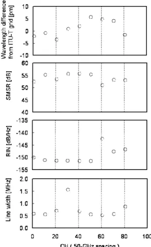
Fig. 10 Lasing wavelength tuning map.
Fig. 12 Measured characteristics of tunable laser module.
the relative intensity noise (RIN) was less than−143 dB/Hz. Spectral line widths at most of the channels were between 0.5 MHz and 1 MHz. Only one channel exhibited a rela-tively large line width value of 1.6 MHz, which is thought to be affected by some electric noise introduced into the SOA gain current. Still, obtained characteristics are sufficient for practical use.
4. Widely Tunable Laser with 100-GHz-FSR Ring Res-onators
As described in Sect. 2.2, there is a design trade off between a tunable wavelength range and a threshold gain difference. A threshold gain difference is an important factor which determines the stability of single-mode lasing without grid hopping. One solution for the trade off is to use the triple ring structure instead of the double ring structure, as pre-viously mentioned in Sect. 2.2. Here, we report on another solution for the trade off, namely, the use of ring resonators with 100-GHz FSR instead of 50-GHz FSR. In Sect. 2.2, an equation is described for the tunable range magnifica-tion factor, M= FSR 2/(FSR 2 − FSR 1). This equation also gives a rough explanation of why the use of 100-GHz-rings solves the design trade off. From this equation, we can derive the second equation, (M× FSR 1) = (FSR 1 × FSR 2)/(FSR 1 − FSR 2). Here, (M × FSR 1) is the
tun-Fig. 13 Transmittance spectra of 50-GHz and 100-GHz FSR single ring.
able wavelength range, and the (FSR 2− FSR 1) value de-termines the transmittance difference (threshold gain differ-ence). Namely, the second equation is a trade-off equation between the tunable wavelength range and the gain di ffer-ence. Using the ring resonators with large FSR values gives a large (FSR 1× FSR 2) value. According to the trade off equation, a larger (FSR1× FSR 2) value gives a larger (M × FSR 1) value for the same (FSR 1 − FSR 2) value (which means a larger tunable range for the same gain difference), or gives a larger (FSR 1− FSR 2) value for the same (M × FSR 1) value (which means a larger gain difference for the same tunable range). Thus, the trade off between the tunable range and the gain difference can be relaxed using larger FSR rings such as 100-GHz rings.
The radius of a 100-GHz-FSR ring is 280μm, which is half the radius of a 50-GHz-FSR ring. In general, a bend waveguide with a smaller curvature radius has a higher ex-cess loss. However, because of the large refractive index contrast of 6% in our SiON-core waveguide, the excess loss was sufficiently suppressed even in the 100-GHz-FSR rings. Figure 13 shows transmittance spectra of single ring res-onators with 50-GHz FSR and 100-GHz FSR. The transmit-tance losses for the 50-GHz and 100-GHz rings were almost the same and small enough for the device application. The compactness of the 100-GHz ring is also an advantage from the viewpoint of mass production. The area of the 100-GHz ring is only 25% that of the 50-GHz ring, thus, the device yield of the silica lightwave circuit chips per wafer becomes much higher when 100-GHz rings are used.
We fabricated a tunable laser with 100-GHz-FSR triple ring resonators. The basic structure of the laser is the same as described in Sect. 2.1. The first ring resonator has a FSR of 100 GHz, which works as a wavelength reference ring. By switching theπ-shift power ON and OFF at the thermo optic heater, the 100-GHz reference ring provides the ITU-T grid with a 50-GHz spacing. The second and the third ring resonators have FSRs that are slightly smaller than 100 GHz. They work as tuning rings using the Vernier effect. The FSRs of the tuning rings determine the theoretical value of the tunable wavelength range of the ring resonators, which was designed to be 95 nm in the fabricated device. The ring-resonator chip size was 2.5 × 3.0 mm2.
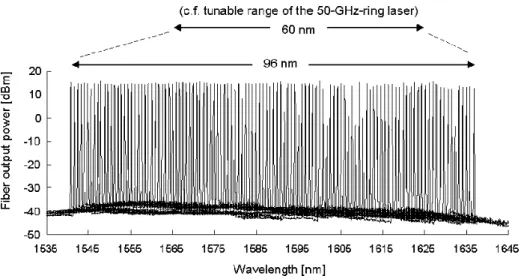
Figure 14 shows superimposed spectra of the fabricated tunable laser. The lasing wavelength range was from 1540 to 1636 nm. The measured tunable range of 96 nm was in good
Fig. 14 Superimposed spectra of tunable laser with 100-GHz-FSR ring resonators.
agreement with the designed tunable range of 95 nm. In this measurement, the channel spacing was 100 GHz; however, a 50-GHz spacing could be obtained with aπ-shift power be-ing applied to the thermo optic heater of the reference rbe-ing. The fiber output power was more than 13 dBm, and the side-mode-suppression ratio was more than 50 dB throughout the whole tuning range. Stable single-mode lasing over a large wavelength region was obtained, which proves the high po-tential of the widely tunable laser with 100-GHz-FSR ring resonators for practical use.
5. Conclusion
We have proposed a tunable laser with silica-waveguide ring resonators. The proposed laser has a simple structure, which is suitable for mass production. The tunable laser exhibits a high fiber-output power of more than 15 dBm and a wide tunable range of 60 nm (L-band, 50-GHz spacing, 147ch). Moreover, a tunable laser with a much wider tunable range of 96 nm with 100-GHz-FSR ring resonators has also been reported.
References
[1] K. Yashiki, K. Sato, T. Morimoto, S. Sudo, K. Naniwae, S. Ae, K. Shiba, N. Suzuki, T. Sasaki, and K. Kudo, “Wavelength-selectable light sources fabricated using advanced microarray-selective epi-taxy,” IEEE Photonics Technol. Lett., vol.16, no.7, pp.1619–1621, July 2004.
[2] Y.A. Akulova, G.A. Fish, P.C. Koh, C.L. Schow, P. Kozodoy, A.P. Dahl, S. Nakagawa, M.C. Larson, M.P. Mack, T.A. Strand, C.W. Coldren, E. Hegblom, S.K. Penniman, T. Wipiejewski, and L.A. Coldren, “Widely tunable electroabsorption-modulated sampled-grating DBR laser transmitter,” IEEE J. Sel. Top. Quantum Elec-tron., vol.8, no.6, pp.1349–1357, Nov./Dec. 2002.
[3] D.J. Robbins, G Busico, L. Ponnampalam, J.P. Duck, P.J. Williams, R.A. Griffin, A.J. Ward, D.C.J. Reid, N.D. Whitbread, and E. Barton, “A high power, broadband tunable laser module based on a DS-DBR laser with integrated SOA,” Tech. Dig. Optical Fiber Communica-tion Conference (OFC), no.TuE3, California, USA, Feb. 2004. [4] D. Anthon, J.D. Berger, and A. Tselikov, “C+L band MEMS
tun-able external cavity semiconductor laser,” Tech. Dig. Optical Fiber
Communication Conference (OFC), no.WL2, California, USA, Feb. 2004.
[5] J. De Merlier, K. Mizutani, S. Sudo, K. Naniwae, Y. Furushima, S. Sato, K. Sato, and K. Kudo, “Full C-band external cavity wavelength tunable laser using a liquid-crystal-based tunable mirror,” IEEE Pho-tonics Technol. Lett., vol.17, no.3, pp.681–683, July 2005. [6] H. Yamazaki, M. Ishizaka, M. Takahashi, S. Watanabe, K. Suzuki,
K. Sato, and S. Sudo, “Widely tunable laser consisting of a sil-ica waveguide double ring resonator connected directly to a semi-conductor optical amplifier,” Proc. 30th European Conf. on Opt. Commun., post-deadline paper no.4-2-4, Stockholm, Sweden, Sept. 2004.
[7] M. Takahashi, Y. Deki, S. Takaesu, M. Horie, M. Ishizaka, K. Sato, K. Kudo, K. Suzuki, T. Kaneko, X. Xu, and H. Yamazaki, “A stable widely tunable laser using a silica-waveguide triple-ring resonator,” Optical Fiber Communication Conference (OFC), postdeadline pa-per PDP19, California USA, March 2005.
[8] Y. Deki, M. Takahashi, K. Suzuki, M. Ishizaka, S. Takaesu, M. Horie, K. Sato, K. Kudo, and H. Yamazaki, “A 160-nm-wavelength tunable laser using a waveguide double-ring resonator,” Proc. 31st European Conf. on Opt. Commun., no.7F3-3, Glasgow, UK, Sept. 2005.
[9] S. Watanabe, M. Takahashi, K. Suzuki, T. Takeuchi, Y. Deki, T. Hatanaka, N. Sakuma, A. Kawauchi, S. Takaesu, M. Horie, T. Miyazaki, M. Kurihara, M. Kanemoto, T. Kaneko, I. Tomita, M. Namiwaka, M. Nido, and H. Yamazaki, “High power tunable resonated-ring-reflector laser using passive alignment technology,” Proc. 32nd European Conf. on Opt. Commun., no.Tu3.4.6, Cannes, France, Sept. 2006.
[10] Y. Deki, T. Hatanaka, M. Takahashi, T. Takeuchi, S. Watanabe, S. Takaesu, T. Miyazaki, M. Horie, and H. Yamazaki, “Wide-wavelength tunable lasers with 100 GHz FSR ring resonators,” Elec-tron. Lett., vol.43, no.4, pp.225–226, Feb. 2007.
[11] R. Todt, S. Watanabe, Y. Deki, M. Takahashi, T. Takeuchi, S. Takaesu, T. Miyazaki, M. Horie, and H. Yamazaki, “Widely tun-able resonated-ring-reflector lasers covering C- and L-bands,” Proc. 33rd European Conf. on Opt. Commun., no.PD2.5, Berlin, Germany, Sept. 2007.
[12] K. Kurata, K. Yamauchi, A. Kawatani, H. Tanaka, H. Honmou, and S. Ishikawa, “A surface mount type single-mode laser module using passive alignment,” Trans. Compon. Packag. Manuf. Technol. Part B, vol.19, no.3, pp.524–531, 1995.
[13] K. Kurata, “Mass production techniques for optical modules,” Proc. 48th Electronic Components and Technology Conference, pp.572– 580, 1998.
Takeshi Takeuchi received his B.E. and M.E. degrees in physical electronics engineering from the Tokyo Institute of Technology in 1988 and 1990, respectively. Since he joined NEC Corporation in 1990, he has been engaged in the research and development of opto-electronic de-vices such as photo detectors and photonic inte-grated circuits. In 2005, he started his work on tunable lasers.
Morio Takahashi received his Ph.D. degree from Tokyo University of Agriculture and Tech-nology in 2001. Since he joined NEC Corpora-tion in 2001, he has been engaged in the research and development of opto-electronic devices.
Kouichi Suzuki received his B.E., M.E. and Ph.D. degrees in electronics and applied physics from the Tokyo Institute of Technol-ogy, in 1995, 1997 and 2000, Tokyo, Japan, re-spectively. Since he joined NEC Corporation in 2000, he has been engaged in the research and development of opto-electronic devices such as planar lightwave circuits for optical communi-cation systems. In 2004, he started his work on tunable lasers.
Shinya Watanabe received his B.E. and M.E. degrees in electronic engineering from Niigata University in 1995 and 1997, respec-tively. Since he joined NEC Corporation in 1997, he has been engaged in the research and development of processes for the waveguides circuits. In 2004, he started his work on tunable lasers.
Hiroyuki Yamazaki was born in Hokkaido, Japan, on March 13, 1964. He received the B.E. and M.E. degrees in electrical engineer-ing from Tokai University, Kanagawa, Japan, in 1986 and 1988, and Ph.D. degrees in electron-ics and applied physelectron-ics from the Tokyo Institute of Technology, in 2007, Tokyo, Japan, respec-tively. Since 1988, he has been with the Opto-electronics Research Laboratories, NEC Corpo-ration, where he was engaged in research and development on semiconductor lasers and opti-cal passive devices for optiopti-cal communications.