九州大学学術情報リポジトリ
Kyushu University Institutional Repository
接触電気抵抗に基づく工具摩耗のインプロセス計測 システムの開発
グアリル, アミン
http://hdl.handle.net/2324/1807020
出版情報:Kyushu University, 2016, 博士(工学), 課程博士 バージョン:
権利関係:
Doctor Thesis March 2017
Amine GOUARIR
Department of Mechanical Engineering Graduate School of Engineering
Kyushu University
Supervisor
Prof. Syuhei KUROKAWA
Development of In-Process Tool Wear Detection
System Based on Electrical Contact Resistance
Table of Contents
Contents………...……….Page No.
Table of Contents ... i
List of Figures ... iv
List of Tables ...x
Abstract….. ... xi
Chapter 1… ...1
INTRODUCTION ... 1
1.1 Introduction ... 1
1.2 Background ... 3
1.3 Problem statement ... 6
1.4 Research Objectives ... 7
1.5 Research Methodology ... 7
1.6 Thesis Organization ... 8
Chapter 2… ...9
EVALUATION OF THE FIRST DEVELOPED SYSTEM ON FACE MILL APPLICATION. ... 9
2.1 Introduction ... 9
2.2 The thermo-electromotive force ... 9
2.3 Electrical contact resistance ... 10
2.4 Methodology ... 15
2.5 Workspace environment ... 17
2.6 Face milling experiment ... 20
2.7 Results and discussion ... 22
2.8 Advantage of the system ... 26
2.9 Conclusion ... 27
Chapter 3… ...29
DETECTION OF TOOL WEAR ON UNCOATED END MILL BASED ON THE ELECTRICAL CONTACT RESISTANCE SYSTEM ... 29
3.1 Introduction ... 29
3.2 Methodology ... 30
3.3 Result and discussion ... 39
3.4 Conclusion ... 43
Chapter 4… ...44
INFLUENCE OF COATING ON ELECTRICAL CONTACT RESISTANCE DETECTION SYSTEM USING COATED END MILL ... 44
4.1 Introduction ... 44
4.2 Methodology ... 45
4.3 Result and discussion ... 49
4.4 Conclusion ... 56
Chapter 5… ...58
NEW DEVELOPED TOOL WEAR DETECTION SYSTEM BASED ON FIBER BRUSH AND SLIP RING TRANSMISSION SYSTEM ... 58
5.1 Introduction ... 58
5.2 Motivation ... 58
5.3 Problem statement ... 59
5.4 Proposed Solutions ... 71
5.5 Experiment using the new developed system ... 85
5.6 Result and discussion of the new system ... 89
5.7 Comparison between Old and the new developed system ... 107
5.8 Result and discussion ... 107
5.9 Advantages of the new developed system ... 114
Chapter 6… ...116
CONCLUSIONS AND FUTURE WORKS ... 116
6.1 Introduction ... 116
6.2 Conclusions ... 116
6.4 Future works ... 118
Acknowledgement ...121
References……….123
List of publications ...136
iv
List of Figures
Figures Page No
Figure 1. Global Overview of tool wear regions ... 4
Figure 2. Seebeck effect ... 9
Figure 3. Measurement of thermal current ... 10
Figure 4. Schematic diagram of a bulk electrical interface (Side view) ... 11
Figure 5. Yellow area shows the real contact spots (Top view). ... 11
Figure 6. Representation of the real contact spots on cutting tool surface (edge) ... 13
Figure 7. Typical presentation of relationship between tool flank wear width and tool-work contact ... 14
Figure 8. Equivalent circuit used in the experimental setup ... 15
Figure 9. Workspace environment and measurements devices. ... 17
Figure 10 . Experimental setup ... 20
Figure 11. Relationship between tool flank wear width and tool contact resistance (with chip breaker) ... 22
Figure 12. Comparison of contact resistance results between tool with and without chip breaker at DOCz= 0.3mm. ... 23
Figure 13. Geometry difference between tool with and without chip breaker. ... 24
Figure 14. Chip breaker function ... 25
Figure 15. Experimental setup 1 for the E.M.F measurement parameters ... 31
Figure 16. The output of the E.M.F. signal according to the following condition: Down cut, DOCy = 8 mm, DOCz = 0.1 mm, Cutting speed = 45 m/min, Feed Rate = 64 mm/min ... 32
Figure 17. E.M.F signal processing according to three cutting speed in down cut. ... 33
v Figure 18. Method of the signal processing for up cut with a following conditions: DOCY
= 8 mm; DOCz = 0.1 mm; Cutting speed = 89 m/min; Feed rate = 128 mm/min ... 34 Figure 19. Method of the signal processing for center cut with a following conditions:
DOCY = 8 mm; DOCz = 0.1 mm; Cutting speed = 89 m/min; Feed rate = 128 mm/min ... 34 Figure. 20. Experimental setup 2, for contact resistance measurement. ... 36 Figure. 21. End milling operation. ... 37 Figure 22. EMF signal processing under the following conditions: Down cut milling,
DOCz = 1 mm, DOCx = 10 mm, Cutting speed = 45 mm/min, Feed rate = 89 mm/min. ... 38 Figure 23. Waveforms of new and worn cutting edges of tool N1 under the following
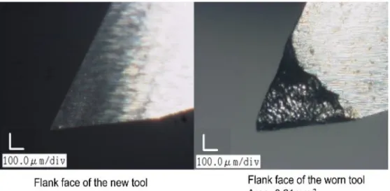
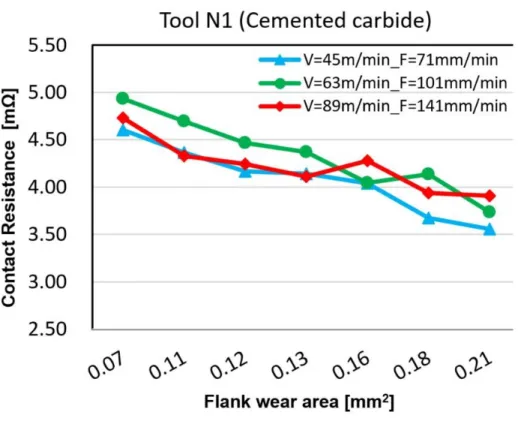
conditions: DOCY = 8 mm; DOCz = 0.3 mm; Cutting speed = 45 m/min; Feed rate = 71 mm/min; Dry cutting ... 39 Figure 24. New and the worn cutting edges of tool N1 captured by a digital microscope. 40 Figure 25. Comparison of tool-work contact resistances at different cutting speeds with
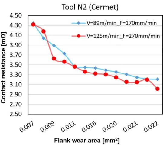
tool N1. ... 41 Figure 26. Comparison of tool-work contact resistances at different cutting speeds with
tool N2. ... 42 Figure 27. Experimental setup for contact resistance measurement. ... 45 Figure 28. End mill operation of coated tool. ... 49 Figure 29. Comparison between tool-work contact resistance under the variation of the
different cutting speed for edge1 of tool N1 ... 50 Figure 30. Comparison between tool-work contact resistance under the variation of the
different cutting speed for edge 2 of tool N1. ... 51 Figure 31. Comparison between tool-work contact resistance under the variation of the
different cutting speed for tool E1 and tool E2 ... 52 Figure 32. New and the worn cutting edges of tool N1 for edge 1 & edge 2 captured by a
digital microscope. ... 53 Figure 33. Relationship between tool-work contact resistance and flank wear area for tool
N2 with a CVD coating. ... 54
vi Figure 34. Relationship between tool-work contact resistance and flank wear area for tool
N3 with a PVD coating. ... 55
Figure 35. The isolation that was used in the experiment. ... 60
Figure 36. Location of the isolation in the experimentation setup ... 61
Figure 37. signal output of voltage drop ... 62
Figure 38. Visual Basic application used to calculate the contact resistance ... 63
Figure 39. Specification of rotary mercury contact ... 65
Figure 40. Experimentation setup of old system with location of the components related to the isolation issue. ... 68
Figure 41. Mercury support unit ... 69
Figure 42. Location of the isolation film ... 71
Figure 43. Isolation film fixed on the tool holder ... 72
Figure 44. Designed carbon brush support ... 75
Figure 45. Carbon brush support realized with 3D printer. ... 75
Figure 46. Carbon brush in action ... 76
Figure 47. Carbon brush after experiment. ... 77
Figure 48. Output signal using single carbon brush ... 77
Figure 49. Silver graphite brush. ... 78
Figure 50. Silver coated ring. ... 78
Figure 51. Double graphite brushes and Coated silver ring in action. ... 79
Figure 52. Double silver graphite brushes and coated silver ring output. ... 80
Figure 53. Ag Cu Coated fiber brush. ... 81
Figure 54. Au Coated slip ring. ... 81
Figure 55. Installation of Ag-Cu Fiber brush and Au slip ring ... 82
Figure 56. Output signal with a coated Ag Cu fiber brush and Au slip ring. ... 83
Figure 57. Fiber brush support unit... 84
Figure 58. Equivalent circuit used in the new experimental setup ... 86
vii
Figure 59. Experimental setup of the new developed system. ... 87
Figure 60. Relationship between tool flank wear area and tool contact resistance under the following condition: DOCy = 5 mm; DOCz = 0.6 mm; F= 170 mm/min and V = 101m/min... 89
Figure 61. Tool N1 (cermet) edge in a new condition ... 90
Figure 62. Tool N1 (cermet) in worn condition. ... 90
Figure 63. Flank wear measurement for Tool N1 (cermet), Area = 0.0526 mm². ... 91
Figure 64. Measured area of flank wear of Tool N1(cermet) highlighted. ... 91
Figure 65. Relationship between tool flank wear area and tool contact resistance under the following condition: DOCy = 5 mm; DOCz = 0.6 mm; F= 170 mm/min and V = 101m/min... 92
Figure 66. Tool N2 (CVD coating) edge in new condition. ... 93
Figure 67. Flank wear of Tool N2 (CVD) in worn condition. ... 93
Figure 68. Flank wear measurement for Tool N2 (CVD) Area = 0.127 mm². ... 94
Figure 69. Measured area of flank wear of Tool N2(CVD) highlighted. ... 94
Figure 70. Relationship between tool flank wear area and tool contact resistance under the following condition: DOCy = 5 mm; DOCz = 0.6 mm; F= 170 mm/min and V = 101m/min... 95
Figure 71. Tool N3 (PVD coating) edge in new condition. ... 96
Figure 72. Flank wear of Tool N3 (CVD) in worn condition. ... 96
Figure 73. Flank wear measurement for Tool N3 (PVD) Area = 0.494 mm². ... 97
Figure 74. Measured area of flank wear of Tool N3 (PVD) highlighted. ... 97
Figure 75. Comparison Tool N1, N2 and N3under the following condition: DOCy = 5 mm; DOCz = 0.6 mm; F= 170 mm/min and V = 101m/min. ... 98
Figure 76. Relationship between tool flank wear area and tool contact resistance under the following condition: DOCy = 5 mm; DOCz = 0.6 mm; F= 170 mm/min and V = 101m/min... 99
Figure 77. Tool N1 (cermet) edge in a new condition. ... 100
Figure 78. Tool N1 (cermet) in worn condition. ... 100
viii
Figure 79. Flank wear measurement for Tool N1 (cermet), Area = 0.051 mm² ... 101
Figure 80. Measured area of flank wear of Tool N1(cermet) highlighted ... 101
Figure 81. Relationship between tool flank wear area and tool contact resistance under the following condition: DOCy = 5 mm; DOCz = 0.6 mm; F= 170 mm/min and V = 101m/min... 102
Figure 82. Tool N2 (CVD coating) edge in new condition. ... 104
Figure 83. Flank wear of Tool N3 (CVD) in worn condition. (Oil test) ... 104
Figure 84. Flank wear measurement for Tool N2 (CVD) Area = 0.755 mm². ... 105
Figure 85.Measured area of flank wear of Tool N2 (CVD) highlighted ... 105
Figure 86. Comparison between tool flank wear area and tool contact resistance under the following condition: DOCy = 5 mm; DOCz = 0.6 mm; F= 170 mm/min and V = 101m/min... 106
Figure 87. Comparison between Old system and New system using Tool N1, under the following condition: DOCy = 5 mm; DOCz = 0.6 mm; F= 170 mm/min and V = 101m/min, (Dry condition). ... 108
Figure 88. Comparison between Old system and New system using Tool N2, under the following condition: DOCy = 5 mm; DOCz = 0.6 mm; F= 170 mm/min and V = 101m/min, (Dry condition). ... 109
Figure 89.Comparison between Old system and New system using Tool N3, under the following condition: DOCy = 5 mm; DOCz = 0.6 mm; F= 170 mm/min and V = 101m/min, (Dry condition). ... 110
Figure 90. Comparison of voltage drop between Old system and New system using Tool N1, under the following condition: DOCy = 5 mm; DOCz = 0.6 mm; F= 170 mm/min and V = 101m/min, (Dry condition). ... 111
Figure 91. Comparison of voltage drop between Old system and New system using Tool N2, under the following condition: DOCy = 5 mm; DOCz = 0.6 mm; F= 170 mm/min and V = 101m/min, (Dry condition). ... 112
Figure 92. Comparison of voltage drop between Old system and New system using Tool N3, under the following condition: DOCy = 5 mm; DOCz = 0.6 mm; F= 170 mm/min and V = 101m/min, (Dry condition). ... 113
ix Figure 93. First example of EMF noise. obtained with a following condition: Tools =
Cermet non coated; Condition of the cutting edge = New, D = 20mm; DOCy = 7.9 mm; DOCz = 0.3mm; FR = 170; V = 101 m/min. ... 118 Figure 94. Second example of EMF in unstable condition obtained with a following
condition: Tools = Cermet non coated; Condition of the cutting edge = New, D
= 20mm; DOCy = 7.9 mm; DOCz = 0.3mm; FR = 170; V = 101 m/min. ... 119 Figure 95. Third example off unstable EMF noise obtained with a following condition:
Tools = Cermet non coated; Condition of the cutting edge = New, D = 20mm;
DOCy = 7.9 mm; DOCz = 0.3mm; FR = 170; V = 101 m/min. ... 120
x
List of Tables
Table 1 Description of the workspace and measurement devices. ... 18
Table 2. Specification of the cutting tools ... 21
Table 3. Specification of face milling operation ... 21
Table 4. Specification of the cutting tools. ... 30
Table 5. Sampling parameters for tool wear detection. ... 35
Table 6. Milling conditions ... 37
Table 7. Specification of the cutting tools end mill ... 47
Table 8. Milling conditions. ... 48
Table 9. Specification of rotary mercury contact ... 66
Table 10. Mercury unit components ... 70
Table 11. Milling conditions ... 86
Table 12. Specification of cutting tools. ... 88
xi
Abstract
This thesis presents the research finding of development of in-process tool wear detection system, which is able to operate under a different type of cutting tools with a different type of geometry and coating, such as face mills, solid square end mills and indexable inserts type under a different application. The performance has been evaluated experimentally. The developed tool wear detection system uses the electrical contact resistance between the tool and workpiece as a gauge to monitor the progression of tool wear. It has been demonstrated in our previous papers that electrical resistance decreases with an increase in contact area on the tool flank. Based on this results, a various experiment has been conducted in our previous studies in order to evaluate and improve the presented tool wear detection system. In fact, high quality of finished surface, optimization of tool life, and accuracy during the cutting process are essential for improving the performance of the manufacturing products and components, thus to achieve this high quality criterions, at first we decided to evaluate and explore the capacity of our first developed system, in order to understand the methodology of the wear detection and the contact resistance measurement in other words, the signal processing, and also to evaluate the further tools which are different from of the experiment obtained previously. The second objective was to evaluate the extension of the interval detection or measurement range to find out the capacity measurement produced by the presented system, based on this chart, a various experiment has been accomplish using a different type of cutting tool with a variation of coating, application, and cutting condition starting by uncoated end mills such as solid square end mill and indexable end mills. In addition, another experiment has been done also for coated solid square end mill and coated indexable end mill. Both experiment has shown great results,
xii which is the consistency of a clear correlation between the progression of electrical contact resistances according to flank wear area.
Our first developed system has a good fundamental method of detection by using simply the electrical contact resistance as an indicator to evaluate the contact wear area.
However, unfortunately it has also some drawbacks and issues, such as the ability to operate under a wet machining or measuring precisely the voltage drop required for the signal processing and the calculation of the contact resistance.
Finally, in this third part of the research a new developed system has been designed to solve all the mentioned issue related to the old transmission system. Which is the problem of the isolation located between the workpiece and the vice of the CNC machine to be able to operate under wet machining and in the same time improve the output signal to improve the quality of the precision measurement. The results of the experiment were evaluated by using the comparisons of the output signals of the old and the new developed system, which was based on relationship between tool flank wear area and tool-work contact
As conclusion, the results of the experiment shows that, the new developed system was very efficient and could accomplished successfully all the objectives of this research.
Now the new developed tool wear detection system based electrical contact resistance is more effective as an in-process tool wear detection system for a different type of tool and able to operate under dry or wet machining.
Keywords—Electric contact resistance, Electromotive force, Flank wear, in- process monitoring, Coating, Square end mill.
1
Chapter 1
INTRODUCTION
1.1 Introduction
Nowadays, the technology of precision machining has attempt a highest level in the history of manufacturing process that has never been reached before in the different field, such as: Automotive, Aerospace, Power Engineering and Medical Engineering fields. The quality of precision machining became one of the most important criteria in manufacturing process. In fact, to answer the stringent load specifications imposed by market challenge, it’s required a full investigation in research and development in order to overcame all problems that manufacturing fields are still facing. Some problems are still persisting until now, especially when it comes to cutting tool such as tool wear which is one of main problems in machining operations.
In fact, the cutting tool wear is highly undesirable in the field of the manufacturing process, because it seriously affects the tool life and the quality of the machined surfaces and causes unpredictable inaccuracy in the work geometry especially in the finished product [1-4]. To avoid such problem, it is necessary that a smart tool wear detection system should be designed to detect the progress of the tool wear during the machining process, so that worn tools can be detected immediately and replaced in time to avoid the interruption of the production planning. This system will save and improve production time, human resources, and production cost [5-8].
A various amount of approaches has been carried out on tool wear monitoring, such as direct tool condition monitoring which is a fundamental requirement for the control of the machining process. Each Tool Condition Monitoring (TCM) method consists of: multiple variations of sensors, amplifiers, signal conditioners and a monitor.
2 The monitor uses a planning to analyze the signals from the sensors in order to provide a reliable detection of tool and process failures. This planning can be equipped with some signal visualization system connected to the machine control [9]. For example, to estimate the progression of the tool wear, two methods are commonly used. The first one is direct measurement, which is placing a digital microscope in front of the tool to evaluate the progression of the wear [10-12]. The second method is indirect measurement, where the target is the tool but the evaluation is based on the roughness of the machined surface. According to the condition of the machined surface, the tool wear will be estimated or forecasted.
We can also refer to other methods of measurement, such as a stylus measurement surface profiler, where the stylus is used to monitor tool flank wear by measuring machined surface roughness. It’s true that the system is more flexible and economic, but such a surface profiler is not an in-process measurement, in addition, it’s time consuming method. All the mentioned systems are based on various combinations of sensors, realized by fixing independent sensors around the tool and workpiece such as acoustic emission (AE) sensors, dynamometer for cutting force, vibrations and speed sensors [13- 15]. However, all those methods are still facing a serious problem of variation in the sensitivity of measurement which depends on each machine configuration, temperature and machine environment. In addition, from the economical point of view, the implementation of those methods requires a very high cost and a stringent maintenance schedule [16-19]. Thus, the purpose of this research is to answer all the mentioned issues by designing an efficient and fast measuring method, flexible, stable, and low-cost sensor, which is essential for in-process tool wear monitoring system.
3
1.2 Background
1.2.1 Tool wear
Tool wear is the progressive deterioration of cutting tools caused by a regular cutting operation. It is a definition often associated with tool bits, or tipped tools that are used in manufacturing process with machine tools [23]. The mechanism of wear can be completely different under different conditions. Thus depend on the conditions the wear take its form [24-27]. There are three main forms of wear are that are well known in the metal cutting process which are: abrasion, diffusion, and adhesion [28].
In adhesion wear, the wear is generated by the fragmentation of welded asperity junctions basically between two metal, in the case of cutting process it’s the workpiece and the cutting tool [29]. Junctions between the tool materials and the chip are formed as part of the friction structure; when these junctions are fractured, small fragments of tool material can be rip out and carried away on the underside of the chip, in other words, the new surface of the workpiece [30-36]. The circumstances that exist in metal cutting process are generally suited to adhesive wear for new material with a clean surface which has not been affected by oxide films, that made the formations of welded asperity junctions easier [37-41].
In the case of abrasive wear, the wear happens when hard fragments on the underside of the chip cross over the tool face and remove tool material via mechanical process [42]. These hard fragments may be highly cold-worked hardened particles of an unstable built-up edge, particles of the hard tool material eliminated by adhesion wear, or hard formation in the work material, as well as oxidation in the work surface [43-49].
Finally, in the case of solid-state diffusion; it’s appears when molecules in a metallic crystal lattice move from a zone of high atomic concentration to one of low concentration [50-53]. This process is dependent on the existing temperature, and the amount of distribution increases in temperature, and the amount of distribution increases
4 exponentially with increase in temperature [54-56]. This action, that takes place within a very precise reaction region at the interface between the workpiece and the tool work and causes a weakening of the surface structure of the cutting tool, is very well known as diffusion wear [57-61].
1.2.2 Forms of wear in cutting process
The progressive tool wear takes place basically in two different ways;
1. Crater wear: it’s the wear on the tool face recognized by the formulation of crater and occurs from the action of the chip passing along the face [62-68].
2. Flank wear: it’s a wear located on the flank where a wear area is formed from the rubbing operation of newly generated workpiece surface. In other words, It’s the wear caused by the friction between the newly machined workpiece surface and the contact area on the tool flank. [69-73].
All attentions in this research were focused on the tool wear region as shown in Figure 1, which is the contact area between the cutting tool and the workpiece.
Figure 1. Global Overview of tool wear regions
5 1.2.3 Tool life optimization
From the economical point of view, in manufacturing process especially cutting metal specifically, cutting tool life is one of the most important considerations. The reason why in roughing operations for example, the cutting speeds, feed rates, and the various tool angles, are usually highly considered and selected to optimize or to give better economical tool life. However, if the parameters mentioned previously are not carefully considered, it will certainly reduce the tool life which is uneconomical because tool replacement or even tool-grinding costs are very high [74]. Furthermore, it’s true that the use of very low feeds and cutting speeds give long tool life but it’s uneconomical because it’s generates a low production rate [75-80]. Certainly, any work material, tool or wear detection system improvements that increase tool life will be very beneficial.
Many approaches have been made over the years to develop in-process tool wear monitoring and also to develop and improved materials with better life [81]. To design a criterion for such improvements, many effort has been made to understand the different forms of tool failure and also the nature of the tool wear [82-88].
The life of a cutting tool can be shortened or ended in various ways, these ways can be divided into two main groups that lead to:
1. Premature end failures, related to the management of configurations related to the cutting parameters.
2. Progressive end failures, or wearing of certain regions of flank or face of the cutting tool.
Tool life can be defined as the cutting time required to reach tool life limitations [89-93]. The most important aspect affecting tool life when the work material, tool material, and tool shape are chosen for a specific machining operation is the cutting speed, in other hand it has been found that machining specifications or parameters may have a secondary effect on tool life [94-97].
6 A tool life pattern is usually defined as a scale to predetermine the value of a tool- wear measure [98]. In machining process, the wear of the flank and the face of the cutting tool is ununiformed along the cutting edge, however, it is important to indicates the degree and locations of the wear when deciding on the quantity of allowable wear before provision of the tool [99-102]. By investigating every details related to the behavior of the tool during the cutting process, in direct or indirect dimensions, this will help us to better deal with tool life extension, an example, the effect of feed and speed [103].
1.3 Problem statement
The problem and difficulty in this research can be divided into four points:
1. The main problem in wear monitoring is in-process detection of flank wear under variations of substrates, coatings and also geometry of the tool itself, and machine tool environment. All those variables must be considered in order to design a universal and efficient tool wear detection system. In addition, understanding the phenomena of the wear also allow us to better anticipate the failure of the cutting tool and extend the capacity of wear detection.
2. It has been demonstrated that our first developed tool wear detection system [115] is able to detect the wear, however the detection was under dry machining only, thus it was unable to operate under wet machining because of the presence of the isolation film between the work piece and the vice.
3. The signal processing of the first developed system was difficult because of the limitation of the sampling interval. The signal processing is static and not able to anticipate fully the variation of the detected signals.
4. The implementation of the first developed system was based on a rotary mercury contact to insure the transmission of the signal from the cutting tool to the measurement unit. This mercury contact needs an access point to the machine, which is not always available with any milling machine.
7
1.4 Research Objectives
The objective of this research is to evaluate the first developed system under new cutting conditions and new type of cutting tools to overcome all the mentioned issues by the following steps:
1. Evaluation of uncoated solid square end mills and uncoated indexable cutting tool.
2. Evaluation of the effect of coating on the system. Coated solid square end mill and indexable cutting tool have been chosen with a different kind of coating.
3. Elimination of the isolation located between the work piece and the vice.
4. Amelioration of the output signal to improve the signal processing.
5. Improvements of the implementation of the wear detection system on the milling machine.
1.5 Research Methodology
The first step is understanding and exploring every single details in the first developed system by experimentation. Experiment on face milling process has been conducted to exploit the measuring method and check the consistency and the stability of the signal output.
The first developed system uses the electrical contact resistance between the tool and workpiece as a gauge to monitor the progression of tool wear. The electrical resistance decreases with an increase in contact area on the tool flank.
To insure the consistency of the experiment, some parameters has been fixed such as cutting speed, feed rate and the depth of cut. Based on the fixed parameters, the experiment is conducted by applying a repetitive down cut operation on the workpiece and the tool work from the new condition until the failure.
8
1.6 Thesis Organization
After the introduction in Chapter 1, Chapter 2 discussed background studies of the old first developed system. Chapter 3 described the Uncoated square end mill experiment including the results and the discussions. Chapter 4 is dedicated to the results of the coated end mill experiment. The new developed system is described in Chapter 5, and finally Chapter 6 summarizes the results of this research and suggests for a future works.
9
Chapter 2
EVALUATION OF THE FIRST DEVELOPED SYSTEM ON FACE MILL APPLICATION.
2.1 Introduction
At this stage of this research, the first step is to evaluate the capability of the detection system. The target in this chapter is to introduce and analyze the global methodology. To understand the function of the detection system, there are two important key words that need to be highlighted, which are thermo-electromotive force (EMF) and electrical contact resistance.
2.2 The thermo-electromotive force
If two different materials are joined at both ends and one end is at a different temperature (Hot junction) than the other (Cold junction) as shown in Figure 2, a current is generated. This phenomenon is well known as the Seebeck effect and is the basis for the thermocouples [104].
This is exactly what occurs in the milling machine during the cutting process. This E.M.F current is considered as a noise in this experiment, which need to be measured
Figure 2. Seebeck effect
10 and subtracted in order to obtain the real final output, which is the contact resistance [105]. The EMF noise can be measured by voltmeter between the vice of the CNC machine and the workpiece as illustrated in Figure 3. As the value of the current is small, an amplifier is used to magnify the current output.
2.3 Electrical contact resistance
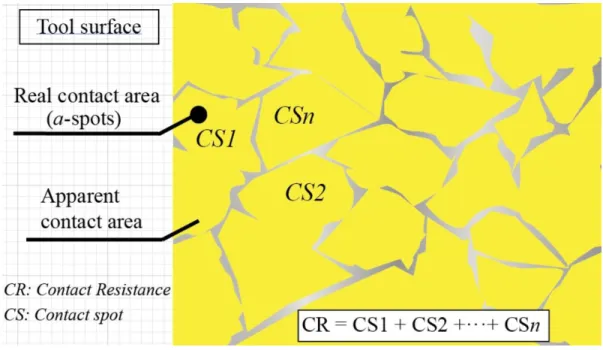
As the measurement of the wear is based on the evaluation of the contact resistance, from a methodological point of view, it’s necessary to review the fundamental of the bulk electrical interface phenomena which is the first link to understand the electrical contact resistance in the presented tool wear detection system [106]. In microscales, all solid surfaces are rough. Surface with micro-roughness consists of peaks and troughs whose shape, variation, height, and others geometrical characteristics, depend on micro-details of the surface generation process [107-109]. The contact between two solids occurs at discrete spots crated by the mechanical contact of two rugged surfaces, as illustrated in Figure 4.
Figure 3. Measurement of thermal current
11 Figure 4. Schematic diagram of a bulk electrical interface (Side view)
Figure 5. Yellow area shows the real contact spots (Top view).
12 The deformation of the surfaces is either plastic, elastic or mixed elastic and plastic, it’s depend on properties of the materials, such as elastic module and also hardness or local mechanical contact stresses [110]. In a bulk electrical interface where usually the coupling components are metals, the contacting surfaces are generally covered with electrically insulation layers or other oxide layers. The interface becomes conductive only when metal-to-metal contact spots are produced, it occurs where the insulating or oxide films are ruptured at the asperities of the contacting surfaces. As shown in Figure 5, typically the real contact area is remarkably smaller than apparent area [111].
Cutting tool can be represented as surface A and workpiece as surface B. The value of the contact resistance will be sensitive to many factors such as variation on the surface of tool flank wear area and workpiece surface roughness, thus every change occurs between the cutting edge and the workpiece such as vibrations, heat, surface roughness should be considered [112].
13 Figure 4 illustrates the theory of bulk electrical interface but in the actual cutting process, the contact stress between tool and work piece is extremely high so the real contact area is larger than yellow area shown in Figure 5, and close to the apparent area shown in Figure 6.
It can be concluded that the deference between real contact area and apparent contact area in the cutting process is very small and negligible. That’s why the contact resistance is used as a gauge to measure the flank wear.
Figure 6. Representation of the real contact spots on cutting tool surface (edge)
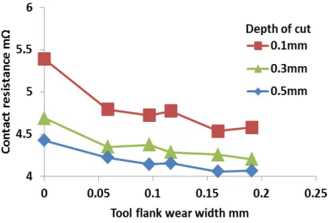
14 As an example, Figure 7 shows a typical relationship between tool flank wear width and tool-work contact resistance obtained in the previous experiments [113-114].
It can be observed that a correlation has been obtained between tool flank wear width and tool-work contact resistance for different depths of cut [115].
Figure 7. Typical presentation of relationship between tool flank wear width and tool-work contact [113].
15
2.4 Methodology
The developed high-speed tool wear detection system uses the contact resistance between the tool and workpiece as a gauge to monitor the progression of tool wear.
The detection method is based on Ohm’s law as shown in Eq (1), where R represents the contact resistance, which is the main indicator of this detection system, V is the voltage, and I is the electric current.
𝑅 = 𝑉/𝐼 (1)
It has been demonstrated in the previous publications that the electrical resistance decreases with an increase in contact area on the tool flank.
Figure 8 illustrates the equivalent circuit used in this experiment, where R1 represents the tool-work electrical contact resistance, R2 is the constant resistance of the measurement circuit, 𝑉𝑚𝑒𝑠 is the measured voltage, and E1 is the electromotive force
Figure 8. Equivalent circuit used in the experimental setup
16 EMF produced by the contact between the tool and the workpiece. SW1 is the MOSFET switch controlled by the sampling program integrated in the microprocessor.
The measurement of flank wear starts when the tool is in contact with the workpiece. If the switch SW1 is in the OFF position, only the EMF voltage E1 is applied to the circuit. As this EMF signal is small and unstable, it cannot be used as a measurement indicator. It should be considered as a noise, which needs to be subtracted from the actual readings. When the switch SW1 is in the ON position, a constant current of 4 A passes through the circuit. This current is produced using a 12 V DC power supply and a resistance of 3Ω. The final voltage required, 𝑉𝑟𝑒𝑞, is obtained by applying the Eq (2).
𝑉𝑟𝑒𝑞 = 𝑉𝑚𝑒𝑠_𝑂𝑁− 𝑉𝑚𝑒𝑠_𝑂𝐹𝐹 (2) Finally, the contact resistance 𝑅𝑐𝑟 can be calculated using Eq. (3) from the values of the current 𝐼𝑡𝑜𝑡 and the voltage required 𝑉𝑟𝑒𝑞. The resistance 𝑅𝑐𝑟 is the sum of R1 and R2. The current 𝐼𝑡𝑜𝑡 is the total current in the entire circuit, which is the sum of the currents produced by the 12 V DC power supply and the EMF.
𝑅𝑐𝑟 = 𝑉𝑟𝑒𝑞
𝐼𝑡𝑜𝑡 (3)
The area of tool flank wear was measured continuously during each cutting operation using a microscope, and the relationship between the actual tool flank wear area and tool-work contact resistance was obtained.
17
2.5 Workspace environment
The experimentation was carried out by, a CNC vertical milling machine ENSHU Figure 9 illustrate the workspace environment and the experimentation setup and describe all the details of the apparatus used for this experiment. In addition to the measurement devices, supplement part and component has been designed and add to the experimentation setup to ensure the functionality of the detection system, such as number (13) rotary contact mercury and its unit located at the top of the CNC milling machine as shown in Figure 9.
Figure 9. Workspace environment and measurements devices.
18 Table 1 Description of the workspace and measurement devices.
Number Descriptions Tasks
1 Monitor of the milling machine
Managing the program and the condition of the milling process.
2 Air extraction Extracting the dust and the excess of oil projected by the lubricant distributor
3 Microscope Monitor Measuring the progression of the flank wear.
4 Amplifier Amplifying the signal output
5 Microprocessor unit or Measurement unit
Signal processing
6 Memory recorder Storing the data
7 Oscilloscope Real time monitoring of signal
output
8 Microscope Observation and measurement of
the flank wear
9 Cutting tool Milling process
10 lubricant Tool life optimization
11 Cutting speed mechanical lever
Changing the rotation speed of the spindle
12 Cables connectors Support the transmission of the current going through the mercury contact
13 Rotary contact mercury Transmission of the current between the tool-work to the measurement unit
19 In Figure 9 it can be noticed that different components have been implemented in the milling machine to ensure the measurement process of the tool wear, between these components there are some important component that need to be highlighted which are:
2.5.1 Magnetic sensor:
Placed on the top of the milling machine. The main function of this magnetic sensor, is to identify the position of the worn tool in the case of the multi-edge tools.
2.5.2 Isolation:
The isolation is placed between the workpiece and the vice of the milling machine, the location of the isolation can be observed in Figure 10. This isolation was add to avoid the short circuit in the measurement system.
2.5.3 Amplifier:
As the measured voltage is very small, the output signal is amplified. by X 200 to ensure a clear representation of the measured signal, which is necessary for the signal processing. The range of the amplification depend firstly on the resistivity of the circuit and also on specification of the cutting tool.
2.5.4 Memory recorder:
It’s used as an oscilloscope for live monitoring and also for recording the amplified output signal. The recording time was not fixed, it can be increased or decreased depend on the need. As an example in the case of noisy signal increasing the record time is benefit to increase the choice of the waveform selection during the signal processing. In the case of this experiment recording time was fixed at 4 second. After recording the data, voltage drop was analyzed measured and the contact resistance was calculated. Meanwhile, the memory recorder was also used as oscilloscope for live monitoring.
20
2.6 Face milling experiment
At this stage of our research, the target was to evaluate the progression of the wear with different tool geometry which is chip breaker in face mill process. Based on this planning, an experiment on face milling process has been conducted. Figure 10 illustrates the experimentation setup used for the face milling process.
Figure 10 . Experimental setup
21 To better evaluate the targeted tools on face mill application, different cutting depth has been applied, which are 0.1mm,0.3mm and 0.5mm respectively. Some parameters were fixed such as cutting speed and feed rate, in order to be able to compare the results. To evaluate the progression of the flank wear, a microscope and oscilloscope were used to insure the measurement of tool wear area progression during the face milling process. Table 2 shows specification of cutting tools used in this experiment and Table 3 illustrates specification of the face mill cutting operation.
Tool number 1 2
Substrate Cermet Cermet
Chip breaker ― With
Table 2. Specification of the cutting tools
Workpiece S45C JIS carbon steel Cutting speed V [m / min] 140
Feed rate f [mm / tooth] 0.1 Depth of cut DOCz [mm] 0.1,0.3,0.5
Cutting fluid Without
Table 3. Specification of face milling operation
22
2.7 Results and discussion
The result of milling operation has been done with two different type of tool and under different depth of cut in the following order (0.1mm), (0.2mm) and (0.5mm). The results shown in Figure 11 illustrates a good correlation between tool contact resistance and tool flank wear width in every depth of cut respectively 0.1mm; 0.2mm and 0.5mm.
It can be seen from the same Figure 11 that in case of deep depth of cut DOCz = 0.5mm, the electrical contact resistance is lower than DOCz = 0.1mm. Similar observation has been obtained previously shown in Figure 7. for the case of two depths of cut; DOCz = 0.5 mm and DOCz = 1mm. This result proves clearly the consistency with the previous experimentations and also with our theoretical explanation regarding the behaviors of the contact resistance with contact area. This similar variation is due to
Figure 11. Relationship between tool flank wear width and tool contact resistance (with chip breaker)
.
23 the contact area of the tool with a workpiece, when the depth of cut is important the contact area between the cutting tool and machining surface will be important and vice versa in the case of small depth of cut.
The last experiment of this step was focused on the geometry difference of the cutting tool. For this reason, two different tool has been chosen: tool with chip breaker and without chip breaker. The experiment has been conducted based on same face mill application and cutting condition, to carry out the comparison between the results of the tools. In this operation the depth of cut was fixed at DOCz = 0.3 mm.
As results it can be noticed from Figure 12 that, the behavior of the electrical contact resistance regarding the flank wear area in the case of chip breaker inserts is similar to cutting edge without chip breaker. In other words, correlation between The contact resistance and flank wear width also exist.
Figure 12. Comparison of contact resistance results between tool with and without chip breaker at DOCz= 0.3mm.
24 However, new different observation has been obtained, which is the contact resistance level. From Figure 12 it can be clearly identified that average of the electrical contact resistance for the insert with chip breaker (Black curve) is lower than tool without chip breaker (red curve). This result is due to the geometry of the tool.
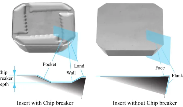
As both tools are uncoated and belong to the same substrate, the evidence of coating effect and substrate can be dismissed. The only different point was the geometry of the tools. Figure 13 illustrates the difference of the geometry between tool with and without chip breaker.
Based on this observation, the result of the difference level of electrical contact resistance can be explained. The contact resistance is lower in case of chip breaker because the contact of the chip with a tool is larger in the case of chip breaker than insert
Figure 13. Geometry difference between tool with and without chip breaker.
25 without chip breaker. During the cutting process, the chip enters inside the pocket, of the chip breaker from the land through the wall to the pocket. As the chip rolled inside the pocket, the contact of the chip surface with a tool surface increase so that contact resistance decrease. Figure 14 illustrates the function of the chip breaker.
The actual function of a chip breaker is to improve control of chip flow during the cutting process in order to reduce cutting resistance. In other words, a good balance between the two will increase the machining performance.
The goal is to brock the chip into suitable lengths, using the chip breaker, will avoid the chip to wrap around the workpiece. In addition, vibration will decrease and tools will not be not damaged easily. Chip breakers function also affect cutting resistance.
By reduced cutting resistance chipping and fracturing of the cutting edge caused by vibration can be avoided. Additionally, lower cutting resistance can decrease the load and heat, and can delay the appearance of tool wear.
Figure 14. Chip breaker function
26
2.8 Advantage of the system
The presented tool wear detection system has many advantages for the manufacturing process because its method is unique and original that can be listed as follow:
a) Originality: various system used the EMF as main signal to detect the wear but unfortunately, the issues with EMF signal is variable and not stable in the case of operating with a different cutting speed. However, the presented system uses the electrical contact resistance as a main indicator to measure the wear, and its more stable because the current applied is under the control.
b) Simplicity: Many approaches have been done on developing a wear detection system However most of those system is based on complex sensors that represents a huge cost in implementation and more for maintenance. The presented system is after all very simple because it does not require multiple expensive sensors.
c) Efficiency: it has been proved through the previous results that same presented system is able to detect the flank wear progression successfully in dry condition.
There are also some disadvantages also that was highly considered, the reason why this dissertation considered the theme as objectives to solve the issues and improve the measurement system through a new developed wear detection system based on the same methodology.
27
2.9 Conclusion
1) The presented tool wear detection system was able to detect the wear on face milling process. A correlation has been obtained between the electrical contact resistance value and tool wear area and without chip breaker.
2) As it has been demonstrated in our previous experiment, the measurement system was able to detect the wear under different cutting depth respectively DOCz = 0.1mm, 0.3mm and 0.5 mm which mean that, contact resistance changes in the case of different depth of cut in other words, the contact resistance increases in the case of large depth of cut. This results, totally agreed with our theoretical expectations, because when the cutting edge plunge deeply into the workpiece, contact area between the cutting tool and the workpiece increases.
3) As the contact resistance is sensitive to the change of cutting depth, the measurement system will be then more suitable and efficient for finishing process.
4) According to the result of the experiment, the variation result of contact resistance between the tool and work piece shows that, even in case of different tool geometry, the contact resistance can be always detectable.
5) After comparing the results of both tools, it has been noticed that our system is also sensitive to the rake face wear and able to detect evaluate it. However, after a deep investigation, it has been concluded that, variations of the rake wear progression are almost more stable comparing to the that flank face, because the forces impact during cutting process are more important on the flank face. Based on this reasoning, it has been decided that, rake face progression value, has to be considered as a constant that will be included in every measurement, and all attention must have to be focused on flank wear.
28 6) Regarding the chip breaker, it has been noticed also that rake face wear progression is better controlled than tools without chip breaker. Based on this conclusion it has been decided that, the chip breaker will be more suitable in our research investigation that tools without chip breaker.
As a conclusion; the present Tool Wear Detection System based electrical contact resistance was effective as in-process detection tool wear system in face milling process and can be applicable.
29
Chapter 3
DETECTION OF TOOL WEAR ON UNCOATED END MILL BASED ON THE ELECTRICAL CONTACT RESISTANCE SYSTEM
3.1 Introduction
This chapter presents a method for in-process tool wear detection in uncoated square end mills applications. This experiment has been carried out with a same tool wear detection system, which uses the contact resistance between the tool and workpiece as an indicator to monitor the progression of tool wear. The electrical resistance decreases with an increase in contact area on the tool flank. In the previous experiment, the target was the face milling process. In this experiment, every attention was focused on uncoated square end mill applying to down cut. The results are presented based on the observations made on the relationship between the area of tool flank wear and tool- work contact resistance. In conclusion, the results of the experiment show that the present tool wear detection system is effective as an in-process tool wear detection system for uncoated square end mills.
In previous experiments, we had studied different aspects of face milling conditions with variations in cutting tools, such as the use of chip breaker. From the results, we could obtain a correlation between the electrical contact resistance and flank wear for each tool [20-21].
This study demonstrates the progression of tool wear in finishing process using an uncoated square end mill under the same high-speed tool wear detection system based on the electrical contact resistance [21].
30
3.2 Methodology
This experiments were divided into two parts: First part was the determination of the sampling parameters and the second part, was dedicated to the measurement of the contact resistance
3.2.1 Determination of sampling parameters:
As the tool is different from the previous experiment, new parameters are also required. Therefore, the objective in this step of the experiment is to update the sampling parameters of the microprocessor program according to the new E.M.F. measurement in the system. Table 4 contains the specification of the tool used in this part of experiment.
To achieve this measurement, a carbon resistance of 70 kΩ was placed between the workpiece and the tool to avoid the high frequency of noise generated by the body of the milling machine as shown in Figure 15. This resistance was chosen specifically based on trial and error to improve the quality of the output signal.
Tool number Tool N1 Tool N2
Base material Cemented carbide Cermet Coating type Non-coating
Diameter 20 mm 20 mm
Helix angle 30° 20°
Corner radius < 0.1mm 0.8mm
Axial rake 30° 8°
Radial rake 1° -20°
Table 4. Specification of the cutting tools.
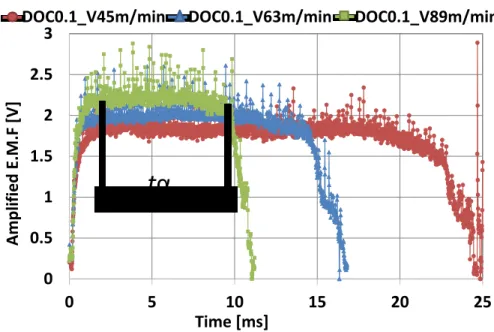
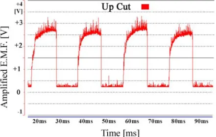
31 Moreover, a different ground conductors have also been connected for the same reason. The voltage drop has been measured according to three cutting speeds which are 45 m/min, 63 m/min, and 89 m/min, and three cutting applications of up cut, down cut and center cut in order to define the common interval 𝑡𝛼.
Figure 15. Experimental setup 1 for the E.M.F measurement parameters
32 The depth of cut was fixed at 0.1mm and the feed rate at 0.045 mm/tooth. The location of the interval 𝑡𝛼 allows us to decide five important parameters for the sampling, as illustrated in Figure 16 and Figure 17 which are:
1) Threshold level 1 𝑉𝑠 : Rising point of E.M.F.
2) Measurement range 𝑡𝛼 where: 𝑡1 + 𝑡2 < 𝑡𝛼. 3) Sampling period of constant E.M.F. 𝑡1.
4) Sampling period of voltage drop to be subtracted 𝑡2. 5) Threshold level 2 𝑉𝑒 : Falling point of E.M.F.
Figure 16. The output of the E.M.F. signal according to the following condition: Down cut, DOCy = 8 mm, DOCz = 0.1 mm, Cutting speed = 45 m/min, Feed Rate = 64 mm/min
![Figure 7. Typical presentation of relationship between tool flank wear width and tool-work contact [113]](https://thumb-ap.123doks.com/thumbv2/123deta/9921426.1921204/28.918.209.726.233.581/figure-typical-presentation-relationship-tool-flank-width-contact.webp)