INVITED PAPER Special Issue on the Past, Present, and Future of Communications Technologies in the IEICE
Optical Transmission Systems Toward Longer Reach and Larger Capacity
Kazuo HAGIMOTO†a),Fellow
SUMMARY This paper reviews long optical reach and large capac- ity transmission which has become possible because of the application of wide-band and low-noise optical fiber amplifiers and digital coherent sig- nal processing. The device structure and mechanism together with their significance are discussed.
key words: optical amplifier, erbium-doped fiber amplifier, high-speed transmission, digital coherent transmission, digital signal processing
1. Introduction
Research and development of optical transmission systems has more than 30 years of its history as shown in Fig. 1.
During the history, transmission capacity has reached ten to the 5th power of magnitude to meet expanding traffic de- mand with corresponding rate. Accordingly, transmission cost has been reduced dramatically and now optical trans- mission systems serves as indispensable infrastructure of the current ICT society. So far, traffic demand is still expand- ing rapidly, therefore optical transmission systems should be also enhanced further to meet such demands.
Looking back the history, the introduction of fiber ca- bles having enormous transmission capabilities is the main driving force to develop optical communication systems[1].
The potentials of single-mode fiber transmission technology also became the motive force in upgrading and improving the performance of optical transmission, optical circuitry, LSI, and relevant technologies, etc. In addition to that, the invention of optical amplification with erbium-doped fiber amplifier seems to have significant impact to accelerate the innovation.
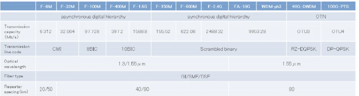
Before the invention of optical amplifiers, large- capacity optical transmission systems F-400M, F-1.6G and their transitions into F-600M, F-2.4G corresponding to syn- chronous digital hierarchy (SDH), have been developed and deployed as shown in Table 1. These systems are named since they use optical fibers as a transmission medium.
In these systems, all the interfaces with optical fibers are through directly modulated laser diodes (LD) and avalanche photodiodes (APD) by which the electro-optic (E/O) and opto-electric (O/E) conversions are carried out. The main devices of these direct modulation/direct detection systems
Manuscript received October 18, 2016.
Manuscript revised January 27, 2017.
Manuscript publicized March 22, 2017.
†The author is with NTT Electronics Corporation, Yokohama- shi, 221-0031 Japan.
a) E-mail: [email protected] DOI: 10.1587/transcom.2016PFI0016
Fig. 1 Transmission systems evolution.
(called IM/DD systems), that is, LDs and APDs can, fortu- nately, operate in the Gbit/s range. Therefore, they could function very well in terms of the transmission speed (data rate) against the already existing coaxial cable based systems (maximum realized speed of DC-400M). The problem in in- creasing their speed was the strictures of the spectrum which caused the Fabry-Perot LDs to be changed to the distributed feedback ones (DFB-LD) and mode distribution noise (opti- cal power fluctuation between several modes) was overcome [2].
To further increase the speed and repeater span, some problems arise. The major one is that besides being a light source, the LD must also function as a modulator and the chirping due to the direct modulation impedes the increases of the speed[3]. Further, the gain bandwidth (GB) product of the detector also is seen to be limited at several Gbit/s operation.
We can address that the difficulties are in multifunc- tional behavior expected from the same device as discussed in Clause 4.2. To remove these obstacles, the two approaches can be considered: (1) research and development of LDs and APDs with improved performance; and (2) separation of the Copyright©2017 The Institute of Electronics, Information and Communication Engineers
Table 1 Specifications of optical transmission systems.
functions and proper assignments to various devices. With regard to the first option, application of ultra-fine grating technologies could made possible 10 Gbit/s transmission to long distances[4],[5]. With regard to the second option, a logical leap to accelerate the progress is to develop the key technologies which boost the advantages of each device.
The optical fiber amplifier can meet the second option mentioned above is considered. Using this technology, not only are the limitations of the detector sensitivity due to shot noise of IM/DD systems improved, but it has also resulted in upgrading the capabilities of each device, repeater structure, and improved flexibilities[6]. Thanks to such capability of optical amplifiers, 10G and 40G transmission systems (FA- 10G, 10G-WDM, and 40G-WDM) have been developed and deployed in the field, successfully. Here, WDM means we use wavelength division multiplexing (WDM) in those sys- tems. The systems plotted along orange, purple, and blue curves are based on IM-DD, optical amplifier WDM, and digital coherent technologies, respectively. Early systems adopted asynchronous digital hierarchy for client accom- modation and network management. After that, SDH and optical transport network (OTN) standards followed recom- mended in ITU-T SG15. In general, when we increase the speed of transmission systems, transmission distance or op- tical reach will be degraded. Thus, more SNR will be re- quired to keep the same level of bit error rate and optical reach. So we need to improve optical transmitter, receiver, and repeaters to overcome the SNR issue. Thanks to the innovation by optical amplifiers, long repeater spacing has been kept constant so far as shown in Table 2.
Figure 2 summarizes the evolution of spectral width as a function of bit rate. As the speed increases, not only does the circuit itself become harder to operate, but the increased bit rate and narrower pulse width also lead to severer conditions related to chromatic dispersion in the fiber (the phenomenon whereby pulses traveling through the fiber gradually broaden out). The reason why speeds have increased smoothly in spite of this is that the original 400-Mbit/s (Fabry-Perot laser diode) systems had a spectral width of about 5–8 nm, or about 600–700 GHz in terms of frequency spreading, which was very wide. In the drive towards increased capacity, signals have been subjected to more and more spectral compression.
As a result, in a 1.6-Gbit/s (distributed feedback laser diode)
Fig. 2 Spectral width as a function of bit rate.
single longitudinal mode system, the data is transmitted with a spectral width of about 0.3 nm, i.e., less than 50 GHz. In the future, the frequency occupancy factor will continue to decrease, reaching about 1 for 10-Gbit/s systems, but modu- lating a 10-Gbit/s signal will result in a bandwidth of about 10 GHz. This is referred to as direct laser modulation, al- though instead of the laser being actually switched on and off directly, its output is modulated on and off by a lithium niobate optical crystal. As the bit rate increases, the overall spectral width of the system conversely decreases. However, this rate is close to the limit of ordinary modulation and demodulation, so the spectral width will increase if the bit rate is made any higher. If this happens, the pulse widths will tend to increase and become more susceptible to the ef- fects of fiber dispersion, and it will become necessary to use dispersion equalization techniques to alleviate this problem.
A variety of modulation and demodulation techniques are also being applied to wireless communications and ADSL (asymmetric digital subscriber line), where it is thought that improvements can be expected in the same way as with op- tical signals by applying similar measures to the modulation and demodulation techniques and by employing digital sig- nal processing techniques.
To go beyond 40G of bit rate, we have to go beyond the purple solid line shown in Fig. 2. The purple line is a transform limit of binary systems; therefore, we need more advanced modulation formats, which have higher spectral
Fig. 3 Optical network evolution.
efficiency such as quadrature phase shift keying (QPSK) and more. Also, more precise compensation of group velocity dispersion (GVD) and polarization mode dispersion (PMD) will be required, since those modulation formats has rather smaller tolerance against such impairments. To overcome these problems, digital coherent signal processing has been invented and developed. With the help of such technology, 100G commercial systems (100G-PTS) are realized and de- ployed.
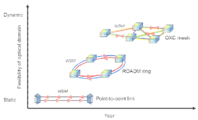
The optical amplifiers also have significant impact on network topology. The early transmission systems deployed in the field environment has a point-to-point link system as shown in Fig. 3. With the help of optical amplifiers, optical passive devices such as optical switches with large dimen- sions and many in/out ports can be utilized in reconfigurable optical add-drop multiplexer (ROADM) node systems. Op- tical loss of such switches can be effectively compensated by optical amplifiers. ROADM systems bring about network topology evolution from point-to-point to ring as shown in Fig. 3, and widely deployed. Remote configuration of net- work with ROADM system has reduced operating cost of photonic network. After that, degree of optical switches have been further extended to support mesh-type optical network for more dynamic and flexible network connections as shown in Fig. 3. Such network can accommodate further dynamic services and have more tolerance against network failures including disaster, since we can establish multiple routes to destination nodes.
In this paper, applications of such optical amplifiers in ultra-high-speed transmission are focused upon and their structure together with the advantages of their use in optical transmission systems is discussed. After that, digital coher- ent technology is discussed for further enhance transmission capacity and reach.
2. Background and Impact of Optical Amplifiers The optical fiber amplifiers amplifies optical signal directly.
To promote its application to high-speed optical transmission systems, semi-conductor laser-diode pumping of Erbium- doped optical fiber (EDFA) is an essential innovation.
Snitzer has proposed fiber amplifier itself[7]. After that, a group of Southampton University reported a version
Table 2 EDFA performance.
with single mode fibers [8]. They have enhanced its effi- ciency and gain. Then, other groups reported its noise figure characteristics and effective pumping methods[9],[10]. At last, semi-conductor laser diode pumping with 1.48µm of wavelength was proposed and confirmed its superior perfor- mance of high efficiency and high gain [11],[12]. At the same time, its application to high-speed optical communica- tion systems are firstly reported[6]. There significant contri- butions have triggered extensive research and development of optical fiber amplifier. Consequently, wide penetration of such technologies followed afterward[13].
Table 2 summarizes EDFA performance. Any prior techniques of optical amplification tend to satisfy only a few subjects shown in this table, but not all the subjects.
The EDFA shows excellent performance for all the param- eters shown in the table. It means EDFA meets all the requirements needed for amplifier application and is promis- ing technology toward actual implementation as a deploy- able product. Looking at the relevant reports[6],[14], they have evaluated system performance in its early stage of re- search. Thus it seems to be rational for the above comment on EDFA. With the help of EDFA, optical communication systems so far face drastic change in various aspects. It includes more fiber launched power and higher receiver sen- sitivity to enhance optical signal to noise ratio and/or optical reach. Moreover, flexibility of system design has also ex- panded, since the EDFA can compensate optical insertion loss of some passive and/or active devices. Without EDFA, these devices cannot be used in actual systems. In addition to that, EDFA keeps low distortion even at large output power;
it is suitable to be deployed as a liner repeater in multi-stage repeated optical transmission systems[15]–[17].
3. Characteristics of EDFA
3.1 Basic Operation
One of the important parameters is amplification efficiency.
To discuss the value, we need to consider energy level dia- gram relevant to EDFA. Figure 4 shows typical energy levels for EDFA. We have some options for pumping wavelengths as shown in the figure. However, the quantum conversion efficiency ζ can be expressed as the Eq. (1). Therefore, we should select pumping wavelength which is closer to
Fig. 4 Energy levels of Erbium3+.
signal wavelength to achieve higher conversion efficiency or namely amplification efficiency. Looking at the Fig. 4, pumping wavelength of 1.48µm will have the highest con- version efficiency.
ζ =λpump/λsignal (1)
Another important parameter of optical amplifier is noise figure (NF). The noise figure is proportional to population inversion factor nsp.. When the pumping energy level is iso- lated and far from adjacent levels, nsp.approaches to 1. That is 3 dB in conventional unit. If we adopt 0.98µm pumping, corresponding noise figure will be close to 3 dB. But it suf- fers smaller conversion efficiency as mentioned above. In the case of 1.48µm pumping, the pumping energy level is close to upper level as shown in Fig. 4, so some portion of distri- bution from the upper level will remain at the pumping level.
As a result, nsp. will exceeds 1. Thus, noise figure will be more than 3 dB. In short, 0.98µm pumping is attractive for excellent noise figure. On the other hand, 1.48µm pumping is advantageous in higher conversion efficiency. In the view- point of saturation output power, it depends on absorption efficiency of pumping wavelength. In this aspect, 1.48µm pumping has higher absorption efficiency and is suitable for high output power applications.
3.2 Configuration
The basic configuration of EDFA is shown in Fig. 5. The optical amplifier consists of Erbium-doped fiber, WDM cou- pler, optical isolator, pumping laser diodes, and optical band- path filters. WDM coupler combines signal and pumping optical signals. There are three options in the configura- tion. They are mainly categorized by the relative direction of pumping and main optical signal. Depending on the options, noise figure and output saturation power will differ. For the application for pre-amplifier, input signal level will be small in usual, and should be amplified immediately to reduce op- tical signal to noise ratio degradation as small as possible.
Therefore, forward pumping scheme shown in Fig. 5(a) will
Fig. 5 Typical configuration of optical amplifiers.
be suitable. On the contrary, for post or booster amplifier application, saturation output power is essential parameter to reserve higher fiber launch power. For such application, backward or bi-directional pumping[19]scheme shown in Fig. 5(b) and (c) would be suitable. For linear repeaters, bi- directional or multi-stage cascaded configuration [20]will be appropriate. We will discuss signal to noise ratio issue in the latter clauses.
3.3 Gain and Bandwidth
One of the significant advantages of EDFA is its ultra- wide amplification bandwidth. In the case of silica glass- based EDFA, they have more than 100 GHz times 30 dB gain-bandwidth product. We can expand the bandwidth with Aluminum co-doping. With regard to pumping wave- length, 1.48µm pumping shows relatively flat amplification bandwidth in comparison to 0.98µm pumping. Moreover, 1.48µm pumping can easily achieve more than 100 mW of pumping power, it is suitable to applications which need rela- tively high output power. As shown in Eq. (1), the theoretical maximum conversion efficiency will be 95%, so it can be ap- plicable to high output power applications. Actually, 86% of conversion efficiency has been confirmed experimentally.
A typical gain-output power characteristic is shown in Fig. 6. Output power gradually saturates around 0 dBm.
Above +5dBm, it has rapidly reduced and corresponding output power reaches constant value. In the viewpoint of signal wavelength, 1552 nm (corresponding to optical fre- quency about 193.1 THz) shows higher saturated output power, since 1535 nm has higher unsaturated gain. Above discussion is based on continuous wave (CW) operation.
Fig. 6 Typical gain-output power characteristics.
Fig. 7 EDFA amplification dynamics.
When we discuss short pulse operation, we only need to use averaged power.
3.4 Dynamic Feature of EDFA
The lifetime of excited state of Erbium ion in EDFA has about 10 ms, therefore, optical input signal which has transition time of less than 10 ms, namely fast enough signal, has no effect from the lifetime. Figure 7 shows EDFA amplification dynamics. The solid circles are the typical operation point of EDFA. The overall gain can be determined along with the dotted curve in Fig. 7, depending on their averaged input power. On the other hand, the response for high-speed signal can be determined by the solid line in Fig. 7. As you can see in the figure, EDFA shows quite linear and distortion-free response for high-speed optical signal. Thanks to this supe- rior amplification characteristic, EDFA is quite suitable for high speed optical communication systems, which requires distortion-free amplification.
Along with the above amplification characteristics, op- tical peak power of amplified short optical pulses can be estimated from their duty ratios. By reducing the duty ratio of optical pulse, we can achieve ultra-high optical peak power as shown in Fig. 8[21]. Accordingly, even in under saturated operation condition, EDFA can amplify optical signal with-
Fig. 8 Short pulse amplification characteristics.
out error rate rise or C/N deterioration [22],[23]. In the same way, we can apply to wavelength division multiplexed signals without inter-channel cross talk under saturated op- eration. These features are fundamental advantage of EDFA in contrast to laser-diode amplifier which has short carrier lifetime.
4. Advantages of Optical Amplifier Systems
4.1 Noise Characteristics
In contrast to electrical amplification where both baseband and carrier amplification are available, optical amplification can be applied to only carrier amplification. In addition to that, noise characteristics of optical amplifier are inher- ently different from electrical one. Thermal noise can be defined by noise temperature and noise bandwidth, so it is independent from signal power. However, in optical case, shot noise comes from photon number fluctuation resulted from Poisson process, thus it depends on optical power it- self and determines absolute value of signal to noise ratio.
In legacy transmission systems without optical amplifiers, receiver sensitivity has been mainly determined by thermal noise in optical receivers. Obviously, when we increase the transmission speed, we will suffer more thermal noise, since we need more bandwidth. On the other hand, the gain- bandwidth product of optical amplifier exceeds 100 THz.
Therefore, we are free from gain-bandwidth product limit and receiver sensitivity is determined by noise characteris- tics itself. We do not need to consider additional deteriora- tion even when we increase the transmission speed. Conse- quently, we can come close to shot noise limit for high speed transmission, by overcoming thermal noise.
When we discuss noise characteristics in amplification of electro-magnetic wave, it is convenient to consider the quantum nature or tendency of the signal. The particle- like quantum tendency can be evaluated by hv/kt (h: Planck constant, v: optical frequency, k: Boltzmann constant, t:
temperature). The main source of noise will be thermal noise and shot noise, as we mentioned in the preceding section.
Fig. 9 Thermal noise spectrum.
We will describe these noise characteristics in the following sections, considering the particle or wave-like behavior.
(1) Thermal noise
The average energy of electro-magnetic wave in vacuum can be express by Planck thermal radiation equation. When we suppose that each photon has discrete energy expressed as mhv (m = 0,1,2, . . .), the energy of each mode can be express by the following equation.
W=Σmhve−mhv/kT/Σe−mhv/kT=hv/(ehv/kT−1) (2) The summation in Eq. (2) runs with m (m = 0∼Infinity).
Here, W becomes kT ifhv ≪ kT. The thermal noise as a function of frequency is shown in Fig. 9. As you can see in the figure, thermal noise vanishes around and above 6 THz of frequency. Below the frequency, thermal noise dominates.
The heterodyne detection scheme in microwave communi- cation systems works under this condition, since both carrier and baseband signal has the same noise characteristics.
On the other hand, in optical communication, there is large frequency difference between carrier and baseband signals. Thus, noise characteristic is completely different. In other word, we can say optical amplifier has changed noise characteristic and determination scheme of signal to noise ratio of communication systems. This is why we can achieve high receiver sensitivity with simple direct detection scheme, which is comparable to heterodyne detection scheme.
The fluctuation of photon number after amplification is resulted from spontaneous emission process during amplifi- cation. This process dominates the SNR after amplification.
This fluctuation component causes beat noise with the am- plified optical signal through direct detection and degrades SNR at baseband signal. Therefore, we can improve the SNR by applying optical amplification which has sufficiently high gain and relatively lower noise in comparison with elec- trical amplification. Consequently, we can achieve higher receiver sensitivity with optical amplification. The fluctua- tion in photon number, namely, shot noise can be amplified by optical amplification up to the level where we can ignore
the thermal noise after direct detection. Therefore, we can overcome the thermal noise and realize shot noise limited receiver sensitivity. This is the very advantage of optical amplifier.
(2) Shot noise
As mentioned above, in the optical frequency where the following condition meets: hv>kT, particle nature of elec- tromagnetic waves dominates. In other word, the shot noise becomes main noise component, which is resulted from Pois- son process. When we suppose ideal photon number counter, we observe no error at the space level, since there is no pho- ton in the level. Only at the mark level (mark means the logic
“1” and has optical power), we will observe errors resulted from shot noise, namely, Poisson fluctuation of photon num- ber. Averaged photon number <n> that achieves the bit error rate of less than 10−9 is 21. This determines the shot noise limit photon number. When the mark ratio (ratio of logi- cal “1” in optical signal) of optical signal is 1/2, this value will be 10. Usually, optical signal will be down-converted via detection circuit and discriminated by electrical decision circuit. The SNR of directly detected optical signal can be estimated by the noise figure (NF) of optical amplification.
The NF can be expressed approximately by the following equation[23].
NF=2nsp (3)
where nspis an inverse population factor. When we suppose 0.98-µm pumping, the NF approaches 1 or 3 dB in decibel unit. This means we can approach only 3 dB degraded re- ceiver sensitivity from shot noise limit one. Thus, optical amplification has great advantage to realize extremely high receiver sensitivity even with direct detection scheme.
4.2 Merits of Optical Amplifiers
One of the significant merits of optical amplifiers is its ultra- wide amplification bandwidth. Legacy limitations such as gain-bandwidth product limit and distortion in signal phase does not apply to optical amplifiers. Moreover, these fea- tures will be still kept under multiple amplifications. Such characteristics yield its wider applications including analog transmission as discussed above [18]. In addition to that, digital transmission is inherently and relatively insensitive waveform distortion, so even after 100 multiple amplifi- cations, signal will not suffer such distortion [17]. This ultra-low noise, low distortion, and high gain amplification characteristics open the wide application of passive optical component. Due to insertion loss of such passive optical de- vices, there had been some limitation. So we have confined multiple functions into a single device such as LD direct modulation and APD, so far. The former has two functions of light source and modulator, and the latter has two func- tions of O/E conversion and pre-amplifier. Optical amplifier has overcome the limitation, and brought about wide flex- ibility in the design of optical repeater systems. Thanks to that, LD direct modulation have been split into LD and
Fig. 10 Optical repeater configuration.
wide-band external modulator, and yielded significant im- provement of transmitter performance. Another important point is its architecture of travelling wave type amplification.
Such travelling wave configuration is basically free from os- cillation issue, and can realize stable operation even at more than 40 dB of gain.
4.3 Issues in System Performance Improvements
The important point to further increase the transmission dis- tance had been the limitation due to chromatic fiber dis- persion. With the help of the optical amplifier in optical transmitter, we can apply external optical modulator with reduced frequency chirping in comparison with LD direct modulation. By using such transmitters, transmission per- formance has been improved considerably. We can extend non-repeated transmission distance and also multi-span lin- early repeated transmission distance. Here, “linearly” means we use repeaters consisted of optical amplifiers only. The transmission distance has been extended up to the chromatic dispersion-limited distance or SNR-limited distance by ac- cumulation of amplified spontaneous emission noise. At this point, chromatic dispersion should be accommodated to further increase transmission distance and will be discussed again in later clause.
4.4 System Experiments
Figure 13 shows optical repeater configuration used in a sys- tem experiment in field environment held in1991[24]. As shown in the figure, optical pre-amplifier adopted forward pumping configuration to achieve low noise feature. On the other hand, we adopted backward pumping for post am- plifier to keep high output power from the repeater. Also we inserted monitoring PDs to support automatic shutdown mechanism for safety reason.
Figure 14 summarizes the field trial route of transmis- sion experiment and basic configuration at the bottom. The route extends up to 320 km between Hamamatsu and To- gasaki as shown in the figure. The LT-MUX is a transmit- ter/receiver set and the output optical power is more than 10 dBm. The receiver sensitivity has achieved−32.0dBm (@ BER = 10−9). By deploying linear repeaters, namely, optical amplifiers with configuration shown in Fig. 10, we have realized successful transmission through 1260 km of
Fig. 11 Field trial route of 10-Gbit/s transmission systems.
Fig. 12 Transmission characteristics.
field installed fibers (two round trip between Hamamatsu and Togasaki). Maximum repeater spacing extends up to 70 km and corresponding maximum span loss is 23 dB.
Figure 15 summarizes transmission performance of the long distance field transmission experiment. The observed power penalty is about 4 dB. By controlling the sign of fre- quency chirp of the LiNbO3, Mach-Zehnder (MZ)-type ex- ternal intensity modulator, we have partially compensated fiber chromatic dispersion[25]. Such counter measure will be discussed in the next clause. However, in this field trial, maximum transmission distance is limited by residual chro- matic dispersion.
5. Dispersion Compensation for Further Increases of Transmission Distance and Speed
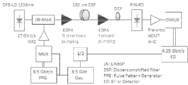
For further increase of the transmission distance and speed, fiber chromatic dispersion equalization will be an issue as discussed in the preceding clause. By applying optical am- plifier as a pre-amplifier in the receiver, we can equalize the group delay caused by the fiber chromatic dispersion without additional power penalty. Such approach has been investigated experimentally at 17 Gbit/s optical signal[26].
Figure 13 shows the basic configuration of the experiment.
Transmitted optical signal is input into pre-amplifier with
Fig. 13 17 Gbit/s 150 km transmission with dispersion compensation.
Fig. 14 Bit error rate characteristics.
forward pumping configuration, and then input to dispersion compensation fiber (DCF) as shown in the figure. With the help of optical pre-amplifier, the SNR of optical signal is de- termined by the input optical power to the amplifier. Thus, we can accommodate group velocity dispersion without any decrease in receiver sensitivity. We used a 150-km fiber of 1.55-µm DSF as a transmission fiber, but we intentionally set signal wavelength at 1.535µm to cause residual chromatic dispersion of about +150ps/nm. The residual dispersion is completely compensated by the inserted DCF which has the same amount of group velocity dispersion of opposite sign. Figure 17 shows transmission performance of the ex- periment. As you can see, we have confirmed penalty-free compensation.
6. Digital Coherent Signal Processing for 100 Gb/s and Beyond Transmission
6.1 Structure of Digital Signal Processing LSI
To realize 100 Gb/s systems, we need more advanced modu- lation formats, which have higher spectral efficiency. Also, more precise compensation of GVD and PMD will be re- quired, since those modulation formats has rather smaller tolerance against such impairments. Multi-level modulation formats generally suffers lower receiver sensitivity and short optical reach. To overcome these problems, digital coherent signal processing has been invented and developed. Co- herent detection enabled through digital signal processing
Fig. 15 Block diagram of coherent DSP.
(DSP) can enhance the level of receiver sensitivity. At the same time, DSP can compensate GVD and PMD in digital circuit[26].
Figure 18 shows a block diagram of the DSP for digital coherent systems. The encoder block receives optical chan- nel transport unit 4 (OTU4) client data from the OTN framer, inserts forward error correction (FEC) parity bits and disper- sion estimator overhead. The encoded data are mapped into a parallel distribution format for optical channel transport lane 4.4 (OTL4.4)[27]for transmission over 4 lanes. The 4 lanes consists of sets of in-phase and quadrature-phase lanes for X- and Y-polarizations. On the decoder side, the 4 lanes of the input analog signals are digitized by a 4-channel analog- to-digital converter (ADC). The frequency domain equalizer (FDE) in the fixed equalizer block compensates for chro- matic dispersion[29]. The cumulated chromatic dispersion of the received signal is estimated within 5 msec, by detect- ing arrival time delay calculated from frequency spectrum of the dispersion estimator overhead. The estimation time does not depend on dispersion amount. An adaptive equal- izer fulfills the roles of polarization de-multiplexing, polar- ization mode dispersion (PMD) accommodation, frequency offset compensation, carrier phase recovery, and sampling clock recovery [30]. Then, the FEC decoder dramatically reduces the number of bit errors. Frame synchronization of OTL4.4 is established within 50 msec, even in the condition that transmission route of optical channel is switched.
6.2 Field Experiment for Fast GVD Compensation We demonstrated fast GVD accommodation in the field en- vironment using the 100 Gbit/s digital coherent signal pro- cessor LSI. The evaluated configuration is shown in Fig. 16.
The transmitted 100 Gbit/s client data from the Ethernet gen- erator are fed into the 100 Gbit/s digital coherent signal pro- cessor LSI. The output digital signals are converted into a PDM-QPSK optical signal through optical front-end. Po- larization division multiplexsing (PDM) means that we use two polarizations as two optical channels with 32-Gbaud of symbol rate. In order to evaluate performance of the LSI in WDM situation, 79 dummy channels of 127.156-Gbps PDM- QPSK signals are also generated. These dummy channels are deployed to evaluate inter-channel cross-talk between WDM signals. The cross-talk includes linear (some optical power leaked from adjacent channels) and nonlinear compo-
Fig. 16 Configuration of the field trial.
nents (optical waveform distortion resulted from nonlinear refractive index of optical fibers). In-phase and quadrature phase lanes of even and odd channels of the dummy signal are individually modulated using the pseudo random binary sequence (PRBS) pattern with a 215−1sequence length with different delays. Then polarization multiplexed with a de- lay of a few tens of symbols to obtain 79-channel PDM- QPSK dummy signal. The test channel is multiplexed with the dummy 79-channel signal through a wavelength selector switch (WSS) to obtain 80 channel WDM signal. The wave- length of the real-time channel under test is 1586.623 nm, which is the center of the WDM signal. Then, the 80 chan- nel WDM signal is launched into the dispersion shifted fiber installed in the field environment. The average fiber launch power is set at−2dBm/ch. The field transmission line con- sists of 6 spans with a 70.4-km repeater section length. The average loss of the 6 spans is 23.2 dB and the accumulated chromatic dispersion is 1,097 ps/nm at 1586.623 nm. On the receiver side, the test channel is WDM-demultiplexed through a WSS, and it is mixed with a local oscillator and converted into a 4 lane electrical signal by an optical front- end based on the planer lightwave circuit technology[31].
The 4 lanes of analog signals are input into the digital co- herent signal processor LSI. The BER is monitored by the 100G Ethernet analyzer.
We measured the Q factor after transmitting an 80 ch WDM signal over 6 spans x 70.4 km fiber. The Q factor is commonly used to evaluate optical signal quality in optical communication systems[32]. The Q factor before FEC for the test channel of 1586.623 nm is measured using the real- time digital coherent signal processor LSI, other channels are measured using the offline configuration. The results are plotted in Fig. 17. Compensation for the chromatic disper- sion is achieved using the dispersion estimator included in the LSI. The received Q-factor before FEC is 9.6 dB. Re- ceived OSNR was approximately 19 dB, and we estimate transmission penalty is approximately 1.5 dB. This indicates that DSP functionalities of chromatic dispersion compensa- tion, PDM demultiplexing, frequency offset compensation, carrier phase recovery, and sampling clock recovery work properly. The measured Q-factor after the FEC is 16.1 dB, which yields error free operation.
As we discussed in the 1stclause, network architecture
Fig. 17 The Q-value and transmitted spectrum.
Fig. 18 Optical signal level received by optical front-end.
will evolve into more dynamic and flexible one to support future applications. So, we evaluate the recovery time, when the optical route is switched. The received signal is switched from the second span to the 6-th span using an optical switch, as shown in Fig. 16. The cumulated amount of chromatic dis- persion changes from 350 ps/nm to 1,097 ps/nm after con- cavity in the optical input level. The sampling clock re- covery block detects the channel disconnection, and informs the sequence controller of the LSI by an alarm pulse. The difference in the cumulated dispersion is estimated, and the sequence controller renews the compensated GVD value in the FDE block according to the estimated value. The OTL4.4 lane alignment alarm disappears after the recovery of the op- tical input signal with the time delay of 12 msec, as shown in lower part of the Fig. 18. In this experiment, total outage time was approximately 15 msec, including the period of no input signal light of 3 msec.
7. Conclusions
With the advent of high-performance optical amplifiers, not only has the transmission ability made a major advance but it has become possible to divide the functions and to use the
potentials of the passive devices. As the result, 10 Gbit/s transmission systems with field performances not different from those of laboratory ones are realized. With regard to the receivers, the limitations due to electronic circuits are greatly relaxed because of application of optical amplifiers. In this way, the realization of much faster signal detectors with very simple structures which were believed to be impossible in the past is now possible. Furthermore, digital coherent sig- nal processing now has been introduced and realized higher receiver sensitivity and fully-automated and instant compen- sation of GVD and PMD. With the DSP, 100G-PTS systems are now widely deployed worldwide. Currently, traffic de- mand is continuing its expansion and also novel services and applications are emerging. Therefore, we need to meet such demand by further technological innovations includ- ing novel modulation, coding, forward error correction, low noise amplifier, and space division multiplexing.
References
[1] S. Shimada, “Research on optical transmission schemes and the fu- ture developments,” NIT R&D, 40, 2, pp.153–160, 1991.
[2] J. Yamada, K. Hagimoto, and N. Ogawa, “F-1.6 G repeaters,” Re- search Report, 36, 2, pp.161–168, Feb. 1987.
[3] K. Hagimoto and K. Aida, “Multigigabit-per-second optical base- band transmission system,” IEEE J. Lightw. Technol., vol.LT-6, no.11, pp.1678–1685, 1988.
[4] S. Fujita, M. Kitamura, T. Torikai, N. Henmi, H. Yamada, T. Suzaki, I. Takano, and M. Shikada, “10-Gbit/s, 100-km optical fiber trans- mission experiment using high-speed MQW DFB-LD and back- illuminated GalDAs APD,” Electron. Lett., vol.25, no.11, pp.702–
703, May 1989.
[5] Y. Miyamoto, K. Hagimoto, F. Ichikawa, M. Yamamoto, and T.
Kagawa, “10-Gbitls, 50-km dispersive fiber transmission experiment using strained multiquantum-well DFB laser diode,” Electron. Lett., vol.27, no.10, pp.853–854, May 1991.
[6] K. Hagimoto, K. Iwatsuki, A. Takada, M. Nakazawa, M. Saruwatari, K. Aida, K. Nakagawa, and M. Horiguchi, “A 212-km nonrepeated transmission experiment at 1.8 Gbit/s using LD pumped Er3+-doped fiber amplifiers in an IM/direct-detection repeater system,” OFC’89, PD-15, 1989.
[7] E. Snitzer, “Proposed fiber cavities for optical masers,” J. Appl. Phys., vol.32, no.1, pp.36–39, Jan. 1961.
[8] S.B. Poole, D.N. Payne, R.J. Mears, M.E. Fermann, and R.I. Laming,
“Fabrication and characterization of low-Ioss optical fibers con- taining rare earth ions,” IEEE J. Lightw. Technol., vol.LT-4, no.7, pp.870–876, July 1986.
[9] R.J. Mears. L. Reekie, I.M. Jauncey, and D.N. Payne, “Low-noise erbium-doped fiber amplifier operating at 1.54µm,” Electron. Lett., vol.23, no.19, pp.1026–1028, 1987.
[10] C.R. Giles, E. Desurvire, J.R. Talman, J.R. Simpson, and P.C.
Becker, “2-Gbit/s signal amplification atλ=1.53µm in an erbium- doped single-mode amplifier,” IEEE J. Lightw. Technol., vol.7, no.4, pp.651–656, April 1989.
[11] E. Snitzer, H. Po, F. Hakimi, R. Tumminell, and B.C. McCollum,
“Erbium fiber laser amplifier at 1.55µm with pump at 1.49µm and Yb sensitized Er oscillator,” OFC’88, PD-2, 1988.
[12] M. Nakazawa, Y. Kimura, and K. Suzuki, “Efficient Er3+-doped optical fiber amplifier pumped by a 1.48µm InGaAsP laser diode,”
Appl. Phys. Lett., vol.14, no.4, pp.295–297, Jan. 1989.
[13] IOOC’89 Post Deadline Session. Proceedings of topical meeting on optical amplifiers and their applications, 1990 and 1991.
[14] K. Hagimoto, Y. Miyagawa, Y. Miyamoto, M. Ohhashi, M. Ohhata, K. Aida, and K. Nakagawa, “A 10-Gbit/s long-span fiber transmission
experiment employing optical amplification technique and mono- lithic IC technology,” IOOC’89, 20 PDA-6, July 1989.
[15] K. Hagimoto, S. Nishi, and K. Nakagawa, “An optical bit-rate flexible transmission system with 5-Tb/s-km capacity employing multiple in- line erbium-doped fiber amplifiers,” IEEE J. Lightw. Technol., vol.8, no.9, pp.1387–1395, Sept. 1990.
[16] S. Saito, T. Imai, and T. Ito, “An over 2200-km coherent transmission experiment at 2.5 Gbit/s using erbium-doped fiber in-line amplifiers,”
IEEE J. Lightw. Technol., vol.9, no.2, pp.161–169, Feb. 1991.
[17] H. Taga, N. Edagawa, Y. Yoshida, S. Yamamoto, M. Suzuki, and H.
Wakabayashi, “10 Gbit/s, 4500 km transmission experiment using 138 cascaded Erdoped fiber amplifiers,” OFC’92, PD-12, Feb. 1992.
[18] E. Yoneda, K. Kikushima, T. Tsuchiya, and K. Suto, “Erbium-doped fiber amplifier for video distribution networks,” IEEE J. Sel. Areas Commun., vol.8, no.7, pp.1249–1256, Sept. 1990.
[19] K. Aida, S. Nishi, Y. Sato, K. Hagimoto, and K. Nakagawa, “Design and performance of a long-span IM/DD optical transmission system using remotely pumped optical amplifiers,” IEE Proc. J, vol.137, no.4, pp.225–229, Aug. 1990.
[20] S. Nishi, K. Aida, and K. Nakagawa, “High efficient configuration of erbium-doped fiber amplifier,” ECOC’90, MoG4.4, Sept. 1990.
[21] A. Takada, K. Iwatsuki, and M. Saruwatari, “Picosecond laser diode pulse amplification up to 12 W by laser diode pumped erbium-doped fiber,” IEEE Photon. Technol. Lett., vol.2, no.2, pp.122–124, Feb.
1990.
[22] K. Hagimoto, K. Iwatsuki, A. Takada, M. Nakazawa, M. Saruwatari, K. Aida, K. Nakagawa, and M. Horiguchi, “250-km nonrepeated transmission experiment at 1.8 Gbit/s using LD pumped Er3+-doped fiber amplifiers in an IM/direct-detection repeater system,” Electron.
Lett., vol.25, no.10, pp.662–663, 1989.
[23] Y. Yamamoto, “Noise and error rate performance of semiconductor laser amplifiers in PCM-IM optical transmission systems,” IEEE J.
Quantum Electron., vol.QE-16, no.10, pp.1073–1081, 1980.
[24] K. Nakagawa, K. Hagimoto, S. Nishi, and K. Aoyama, “A bit-rate flexible transmission field trial over 300-km installed cables employ- ing optical fiber amplifiers,” OAA’91, PD-12, July 1991.
[25] K. Masuda, A. Takada, J. Nakajima, N. Nishi, and K. Aida, “Inves- tigations on configuration of linear repeaters with bit flexible optical amplifiers,” National Conventional Records, IEICE Japan, SB-9-2, Spring, 1992.
[26] E. Yamazaki, S. Yamanaka, Y. Kisaka, T. Nakagawa, K. Murata, E. Yoshida, T. Sakano, M. Tomizawa, Y. Miyamoto, S. Matsuoka, J. Matsui, A. Shibayama, J. Abe, Y. Nakamura, H. Noguchi, K.
Fukuchi, H. Onaka, K. Fukumitsu, K. Komaki, O. Takeuchi, Y.
Sakamoto, H. Nakashima, T. Mizuochi, K. Kubo, Y. Miyata, H.
Nishimoto, S. Hirano, and K. Onohara, “Fast optical channel recov- ery in field demonstration of 100-Gbit/s Ethernet over OTN using real-time DSP,” Opt. Express, vol.19, no.14, pp.13179–13184, 2011.
[27] K. Hagimoto, Y. Miyamoto, T. Kataoka, K. Kawano, and M.
Ohhata, “A 17-0 bit/s long-span fiber transmission experiment us- ing a low..noise broadband receiver with optical amplification and an equalization,” Topical Meeting on Optical Amplifiers and Their Applications, TuA 2, Aug. 1990.
[28] Telecommunication standardization sector of International telecom- munication union (ITU-T), Transmission system and media, digital system and networks G.709.
[29] K. Ishihara, T. Kobayashi, R. Kudo, Y. Takatori, A. Sano, E.
Yamada, H. Masuda, M. Matsui, M. Mizoguchi, and Y. Miyamoto,
“Frequency-domain equalization without guard interval for optical transmission systems,” Electron. Lett., vol.44, no.25, pp.1480–1482, 2008.
[30] T. Hoshida, H. Nakashima, T. Tanimura, S. Oda, Z. Tao, L. Liu, W. Yan, L. Li, and J.C. Rasmussen, “Network innovations brought by digital coherent receiver,” Optical Fiber Communication and Na- tional Fiber Optic Engineers Conference 2010, paper NMB4, 2010.
[31] Y. Sakamaki, H. Yamazaki, T. Mizuno, T. Goh, Y. Nasu, T.
Hashimoto, S. Kamei, K. Hattori, H. Takahashi, T. Kobayashi, and
M. Ishikawa, “Dual polarisation optical hybrid using silica-based planar lightwave circuit technology for digital coherent receiver,”
Electron. Lett., vol.46, no.1, pp.58–60, 2010.
[32] N.S. Bergano, F.W. Kerfoot, and C.R. Davidson, “Margin measure- ments in optical amplifier systems,” IEEE Photon. Technol. Lett., vol.5, no.3, pp.304–306, March 1993.
Kazuo Hagimoto received a B.S. and an M.S. in Electrical Electronics Engineering from Tokyo Institute of Technology in 1978 and 1980, respectively. He joined the Yokosuka Electro- Communication Research Center of Nihon Tele- graph and Telephone Public Co. in 1980. Since then, he has been involved in research on re- alization of high-capacity transmission systems.
Presently, he is the President of NTT Electronics Corporation. He received the K. Sakurai Award from the Association of Optical Technology in 1989, the Oliver Lodge Premium of lEE in 1991. Also, He received purple ribbon prize from the Imperial Majesty of Japan. He is a fellow of IEEE and IEICE.