INVITED PAPER
Special Section on Leading-Edge Applications and Fundamentals of Superconducting Sensors and DetectorsLow-Energy Optical-to-Electrical Converters Based on
Superconducting Nanowire for Single-Flux-Quantum Circuits
Kemmei KAJINO†a),Nonmember, Shigehito MIKI†, Taro YAMASHITA†,andHirotaka TERAI†,Members
SUMMARY We report the energy-efficient optical input interface using NbN superconducting nanowire-based optical-to-electrical (SN- OE) converters for a single-flux-quantum (SFQ) data processing system.
The SN-OE converters with small active areas ranging from 1×1 to 10×10µm2were fabricated to improve the recovery time by reducing the kinetic inductance of the nanowire. The SN-OE with the smallest area of 1×1µm2showed the recovery time of around 0.3 ns, while its detection efficiency for a single photon was reduced below 0.1% due to insufficient coupling efficiency with a single-mode optical fiber. However, the optical power dependence of the error rate of this device showed that the required optical power to achieve the error rate below 10−12at 10 GHz operation is as large as 70µW, which is still one order of magnitude lower than semi- conductor photo diodes. We also demonstrated the operation of the SN-OE converters combined with the SFQ readout circuit and confirmed the oper- ating speed up to 77 MHz.
key words: superconductor, single photon detector, single-flux-quantum circuit, optical interface, cryocooler implementation
1. Introduction
Single-flux-quantum (SFQ) circuits [1] that can integrate over ten thousand of niobium-based Josephson junctions have been demonstrated at clock frequencies of tens of gi- gahertz with a power consumption of only a few milliwatts [2]. Owing to their high-speed and low-power operation, SFQ circuits could be a promising candidate as an alter- native technology for semiconductor CMOS devices, even including the cooling cost. To realize a practical system us- ing this technology, the input/output (I/O) links between the SFQ circuits and the room-temperature electronics are one of key issues to be developed.
So far, a total I/O data rate of 40 Gbit/s (10 Gbit/s×4) has been successfully demonstrated using copper-based coaxial cables [3]. However, these coaxial cables are also good thermal conductors and provide a thermal load of ap- proximately 25 mW per channel, making it difficult to main- tain a low operation temperature with an increase in the number of I/O links. Thus, optical I/O links are desir- able because they can drastically reduce the thermal load to the cooling system. To realize optical I/O links with a high data rate and low energy consumption, energy-efficient and high-speed optical-to-electrical (O/E) converters are an essential component at the input link. Although optical
Manuscript received July 14, 2014.
Manuscript revised October 3, 2014.
†The authors are with Advanced ICT Research Institute, Na- tional Institute of Information and Communications Technology, Iwaoka, Kobe, 651-2492, Japan.
a) E-mail: [email protected] DOI: 10.1587/transele.E98.C.227
input links using uni-traveling-carrier photodiodes (UTC- PDs) and metal–semiconductor–metal photodiodes (MSM- PDs) have been demonstrated [4], [5], the required optical input powers to achieve a sufficiently small bit-error rate were 4.5 mW and 0.75 mW, respectively, which are almost comparable with the power dissipated by the SFQ circuits with ten thousand of Josephson junctions. More energy- efficient O/E converters are required for the realization of future large-scale systems.
Superconducting nanowire single-photon detectors (SSPDs) [6] are promising single-photon detectors with a high system detection efficiency (SDE) of 80% at a wave- length of 1550 nm [7]–[9]. Their high photosensitivity is very attractive for energy-efficient O/E converters operat- ing in a cryogenic environment. However, the counting rate of conventional SSPDs is limited by a large kinetic induc- tanceLk due to the long meandering nanowire to realize a large active area for efficient optical coupling and a high SDE [10]. Further, practical SSPDs with active areas of 10×10 to 15×15 µm2 have Lk =1–2 µH [8], [9], [11], and their maximum counting rate is approximately several tens of megahertz, which is far from the gigahertz rate ex- pected intrinsically. Therefore, a reduction inLk is neces- sary to realize fast O/E converters with a data rate greater than 1 Gbit/s per channel. Although the simplest way to re- duceLkis to reduce the active area as much as possible, this will cause a degradation in the optical coupling efficiency and SDE. To realize low energy consumption and high- speed O/E converters by using SSPDs, the actual nanowire structure should be optimized for the O/E converters with design guidelines that are different from those of conven- tional SSPDs.
In this paper, we report a systematic investigation of the properties of superconducting nanowire-based O/E (SN- OE) converters. We characterize the recovery time and re- quired optical power for error-free operation of the SN-OE converters with various active areas. We also demonstrate the operation of an SN-OE converter connected with an SFQ readout circuit.
2. Experimental Setup
First, we deposited a 9-nm-thick niobium nitride (NbN) film on a 2-inch thermally-oxidized silicon wafer by reac- tive dc-magnetron sputtering [12]. The wafers were then patterned into a meandering nanowire structure by direct electron-beam lithography and reactive ion etching. We fab- Copyright c⃝2015 The Institute of Electronics, Information and Communication Engineers
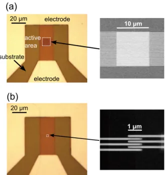
Fig. 1 Optical photomicrographs of the SN-OE converter devices and scanning electron microscopy (SEM) images of the meandering nanowires with active areas of (a) 10×10µm2and (b) 1×1µm2.
ricated devices with active areas of 1×1, 2×2, 3×3, 5×5, and 10×10µm2 on the same wafer. The line width and the space between the nanowires were 100 nm for all de- vices. For simplicity, an optical cavity structure, as reported elsewhere, was not employed in this experiment [11], [13].
Figure 1 shows an optical photomicrograph of the SN-OE converters and a scanning electron microscopy (SEM) im- age of the meandering nanowire pattern with an active area of (a) 10×10µm2 (b) 1×1µm2. Further details of the fab- rication process are described elsewhere [12]. Table 1 sum- marizes the electrical properties of the fabricated devices in the present work. The relatively small distributions of the critical temperatureTcand the critical currentIcsuggest that the uniform superconducting properties of the fabricated de- vices do not depend on the size of the active area.
The fabricated SN-OE converters were mounted into compact fiber-coupled packages using fiber-spliced graded index (GRIN) lenses. Because the GRIN lenses are designed for efficient optical coupling with our conventional SSPDs at 15×15µm2, the beam waist at the active area is approxi- mately 9 µm in diameter [14]. The detailed device packag- ing and implementation procedures are described elsewhere [13]. The fiber-coupled packages were then implemented in a Gifford–McMahon (GM) cryocooler with a cooling ca- pacity of 0.1 W. During the measurement, the temperature of the workspace was maintained at 2.3 K.
3. Experimental Results
3.1 Characterization of the Recovery Time with Various Active Area Sizes
In order to characterize the recovery time of the SN-OE con-
Table 1 Nanowire lengths, critical temperatures, and critical currents of SN-OE converters with various active areas.
Active area Nanowire length Tc Ic
(µm2) (µm) (K) (µA)
10×10 500 7.76 22.6
5×5 125 7.74 22.1
3×3 45 7.74 21.8
2×2 22 7.64 20.6
1×1 5 7.75 21.4
Fig. 2 Kinetic inductances as a function of the nanowire length obtained from the waveform (open circles) and those by using a network analyzer (closed circles). The solid line is a guide for the eye. Inset: Output pulse waveforms of SN-OE converters with active areas of 5×5µm2and 1×1µm2.
verters with various active areas, we measured the depen- dencies ofLkon the nanowire length of the SN-OE convert- ers, as shown in Fig. 2. In this figure, the open circles indi- cate values of Lk obtained from fitting the observed output waveforms of the SN-OE converters by using a simple equa- tion with a recovery time constantτ(=Lk/RL, whereRLis the input impedance on the load side) [10]. To observe the output waveform accurately, the output signals were ampli- fied by two broadband amplifiers (SHF100AP) with a band- width of 30 kHz–23 GHz and acquired by a digital oscil- loscope with an 8-GHz bandwidth (Agilent DSO80804A).
The closed circles in Fig. 2 indicate values of Lk obtained from measurements of the phase of the reflection coefficient S11 =(iωLk−50Ω)/(iωLk+50Ω) by using a network an- alyzer [15]. From these results, it is clear that Lk is pro- portional to the nanowire length and could be reduced to 10 nH by reducing the active area to 1×1µm2. Further- more, the pulse widths of the observed output waveforms are apparently reduced, as shown in the insets in Fig. 2, and the recovery time for the smallest 1×1µm2 SN-OE con- verter was reduced to 0.3 ns.
3.2 Verification of the Required Optical Power for Error- Free Operation
Next, we measured the photon-number dependence of the error rates (ERs) of our SN-OE converters to estimate the optical input power required to achieve error-free operation.
In this measurement, the ER is given by the probability that
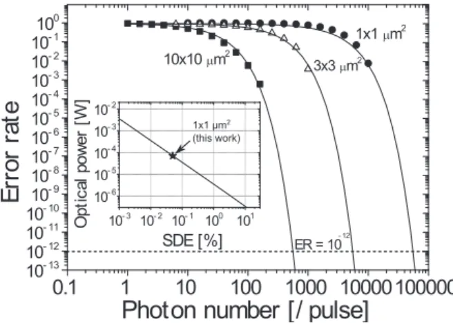
Fig. 3 Error rates of 10×10µm2(closed squares), 3×3µm2(open trian- gles), and 1×1µm2(closed circles) SN-OE converters as a function of the input photon number per pulse at a bias current of 18µA. The solid curves are theoretical curves [Eq. (1)] with SDEs of 4.8%, 0.5%, and 0.05%. Inset:
The optical power as a function of the SDE, where the SN-OE converter operates at 10 GHz with an ER of 10−12.
the device does not respond to an optical signal, and we de- fine error free as an ER less than 10−12[5]. Prior to the ER measurement, we measured the SDE for a single photon at a wavelength of 1550 nm [15]. The SDEs for the active areas of 10×10µm2, 3×3µm2, and 1×1µm2 were 4.8%, 0.5%, and 0.05% at a bias current of 18µA with a dark count rate lower than 1 c/s, respectively. The reduction in the SDE for smaller active areas is simply due to the reduction in the optical coupling efficiency by reducing the active area.
Then, we measured the photon-number dependence of the ERs. A 20-ps-wide pulsed laser diode with a repeti- tion frequency of 1 MHz was used as the input source. The number of incident photons per pulse was controlled by an optical attenuator, and the output pulses from the SN-OE converter were measured by a pulse counter. ERs were then obtained by 1−q/f, whereqand f are the number of out- put pulses per second and the repetition frequency of the input optical pulses, respectively. The results for the SN-OE converters with active areas of 10×10µm2, 3×3µm2, and 1×1µm2 are plotted in Fig. 3, where the bias current was set at 18µA for all devices. Here, the ER is theoretically given by
ER=(1−SDE)m, (1)
wheremis the input photon number per pulse. The solid lines in Fig. 3 are the curves calculated using Eq. (1), where we employed the experimentally obtained values of the SDEs for the devices with each active area. As clearly shown in this figure, the experimental results are well ex- plained by the theoretical curves without any fitting param- eters. Focusing on the result for the smallest active area of 1×1µm2, the required value of m to achieve an ER of 10−12 is estimated to be 54,000 photons per pulse. If we assume an operating frequency of 10 GHz, the optical power consump- tionP, which is given byP=Ephoton×m× f, is estimated to be 70µW at 1550 nm. Even for the SN-OE converter with an SDE of 0.05%, the optical power required to achieve
an ER less than 10−12 is as large as 70 µW, which is still one order of magnitude lower than that of semiconductor photodiodes. This higher SDE will provide a lower optical power for error-free operation. The required optical power to achieve error-free operation at 10 GHz as a function of the SDE is shown in the inset of Fig. 3. The beam-spot diameter in our experimental setup is 9 µm [14], which is much larger than our smallest active area of 1×1µm2. Even if the cen- ter of the beam spot is perfectly aligned with the active area, the optical coupling efficiency is as large as 2.4% accord- ing to a simple calculation using a Gaussian beam profile [13]. O’Connor et al. has reported that the full width at half maximum spot size was reduced to 1.3 µm using a confocal microscope system with an aspheric lens [16]. If we apply this configuration to our 1×1µm2 SN-OE converter, the coupling efficiency will be improved to 77%. In addition, we employed no cavity structure to simplify the fabrication process; however, the SDE of our SN-OE converters will be further improved by employing a cavity structure. We have already demonstrated an SDE of 80% for SSPDs with a double-sided cavity structure [8], [9], which is significantly higher than the SDE below 10% for the SSPD without a cav- ity structure. By employing these techniques to enhance the SDE of the small-area SN-OE converter, an optical power less than 10µW will be possible to realize an ER less than 10−12at 10-GHz operation.
3.3 Operation of the Small-Area SN-OE Converter Con- nected to an SFQ Readout Circuit
To verify the correct operation of SN-OE converters con- nected with SFQ circuits, we implemented the SN-OE con- verter with an SFQ readout circuit in a cryocooler sys- tem and observed the output signals from the SFQ circuit.
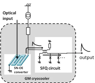
The SFQ readout circuit was fabricated using a clean room for analog–digital superconductivity (CRAVITY) and a 2.5- kA/cm2Nb standard process [17]. The output pulses from the SN-OE converter were converted into SFQ pulses by the front-end circuit called the magnetically coupled DC/SFQ (MC-DC/SFQ) converter, which has an input transformer with a 50-Ωload resistor in series to enhance the input cur- rent sensitivity [18]. After an appropriate signal process- ing, the SFQ pulses are converted into the voltage pulses with the amplitude of approximately 1.8 mV and the dura- tion of 0.8 ns to be detected by the room temperature elec- tronics. The SFQ circuit with a simple merging function of four input channels was used in this experiment, whose detailed operation is described in [18]. The SN-OE convert- ers with an active area of 3×3µm2 and the SFQ chips are implemented in the same workspace in the GM cryocooler and connected via 10-cm coaxial cables, as illustrated in Fig. 4 [19]. In this measurement, a continuous-wave laser was used as the input source. The incident photons sporad- ically arrive to the device. In this case, the incident photons sporadically arrive to the device, and the period of arriving photons can be regarded as the inverse of incident photon rate in average. Therefore, the operating speed of the SN-
Fig. 4 Schematic of the experimental setup of an SN-OE converter and SFQ readout circuits in a GM cryocooler.
Fig. 5 Output count rate as a function of the incident photon rate for a 3×3µm2SN-OE converter connected with the SFQ readout circuit for a bias current of 18µA.
OE converter can be estimated by statistical measurement of the output counting rate from the SFQ readout circuit as a function of incident photon rate [9].
Figure 5 shows the output count rate as a function of the incident photon rate, where the bias current to the SN-OE converter was set to 18µA. For the low-incident-photon- rate region, the output count rate is proportional to the in- cident photon rate, indicating that the mean time interval of each incident photon is longer than the recovery time of the SN-OE converters. Because an SDE of 0.5% can be ob- tained in this region, which agrees with those without the SFQ circuit, the SN-OE converter correctly functioned as an optical input link for the SFQ circuit. In addition, a de- viation from the linear dependence can be observed in the region with a high incident photon rate around 100 MHz be- cause the SN-OE converter cannot follow the photons that arrive when its time interval becomes as short as the recov- ery time. The 3-dB roll-offoperating speed f3dBcan be es- timated from the counting-rate measurement, and this op- erating speed was estimated to be f3dB = 77 MHz for our
3×3µm2 SN-OE converter, which is faster than that of con- ventional SSPDs with larger active areas [9]. However, the Lkof the 3×3µm2 SN-OE converter estimated from Fig. 2 is as large as 40 nH, which gives the recovery time of 0.8 ns.
If the counting rate of our 3×3µm2 SN-OE converter is simply limited by the recovery time, the f3dBis expected to exceed 500 MHz, which is significantly larger than 77 MHz actually observed in our experiment. This suggests that the counting rate of the small-area SN-OE converter is limited not only by the recovery time but also the other mechanism.
Further effort to reveal this mechanism will be necessary for improving the operating speed of SN-OE converter.
4. Conclusion
In this work, we systematically fabricated and characterized NbN SN-OE converters for the energy-efficient optical input interface for SFQ readout circuits. SN-OE converters with the active areas ranging from 1×1 to 10×10µm2 were measured in a GM cryocooler system. The observed re- covery time was improved by reducing the kinetic induc- tance, and a time constant of 0.3 ns was obtained for the smallest SN-OE converter area of 1×1µm2. The photon- number dependence of the ER revealed that the input op- tical power required for the error free operation was ap- proximately 70µW assuming 10-GHz repetitive frequency, which is over one order of magnitude lower than conven- tional semiconductor photodiodes. Further improvements in the energy efficiency can be achieved by improving the optical coupling efficiency and/or adopting an optical cavity structure. We also tested a 3×3µm2SN-OE converter con- nected with an SFQ readout circuit and confirmed the suc- cessful operation at maximum operating frequency of ap- proximately 77 MHz.
Acknowledgments
The authors thank Saburo Imamura and Makoto Soutome of the National Institute of Communications Technology for their technical support. This work was supported by JST- ALCA.
References
[1] K. K. Likharev and V. K. Semenov, “RSFQ logic/memory fami- ly: A new Josephson-junction technology for sub-terahertz-clock- frequency digital systems,” IEEE Trans. Appl. Supercond., vol.1, no.1, pp.3–28, Mar. 1991.
[2] A. Fujimaki, M. Tanaka, T. Yamada, Y. Yamanashi, H. J. Park, and N. Yoshikawa, “Bit-serial single flux quantum microprocessor CORE,” IEICE Trans. Electron., vol.91-C, no.3, pp.342–349, Mar.
2008.
[3] Y. Hashimoto, S. Yorozu, Y. Kameda, A. Fujimaki, H. Terai, and N. Yoshikawa, “Implementation of a 4×4switch with passive inter- connects,” IEEE Trans. Appl. Supercond., vol.15, no.2, pp.356–359, June 2005.
[4] S. Shinada, H. Terai, Z. Wang, and N. Wada, “1550 nm band opti- cal input module with superconducting single-flux-quantum circuit,”
Appl. Phys. Lett., vol.96, no.18, pp.182504, May 2010.
[5] H. Suzuki, “Evaluation of uni-traveling carrier photodiode perfor-
mance at low temperatures and applications to superconducting elec- tronics,” in Photodiodes-Communications, Bio-Sensings, Measure- ments and High-Energy Physics, ed J.-W. Shi, InTech, 2011.
[6] G. N. Gol’tsman, O. Okunev, G. Chulkova, A. Lipatov, A. Se- menov, K. Smirnov, B. Voronov, A. Dzardanov, C. Williams, and R. Sobolewski, “Picosecond superconducting single-photon optical detector,” Appl. Phys. Lett., vol.79, no.6, pp.705–707, Aug. 2001.
[7] F. Marsili, V. B. Verma, J. A. Stern, S. Harrington, A. E. Lita, T. Ger- rits, I. Vayshenker, B. Baek, M. D. Shaw, R. P. Mirin, and S. W. Nam,
“Detecting single infrared photons with 93% system efficiency,” Nat.
Photonics, vol.7, no.3, pp.210–214, Feb. 2013.
[8] S. Miki, T. Yamashita, H. Terai, and Z. Wang, “High performance fiber-coupled NbTiN superconducting nanowire single photon de- tectors with Gifford–McMahon cryocooler,” Opt. Express, vol.21, no.8, pp.10208–10214, Apr. 2013.
[9] T. Yamashita, S. Miki, H. Terai, and Z. Wang, “Low-filling-factor superconducting single photon detector with high system detec- tion efficiency,” Opt. Express, vol.21, no.22, pp.27177–27184, Nov.
2013.
[10] A. J. Kerman, E. A. Dauler, W. E. Keicher, J. K. W. Yang, K. K.
Berggren, G. Gol’tsman, and B. Voronov, “Kinetic-inductance- limited reset time of superconducting nanowire photon counters,”
Appl. Phys. Lett., vol.88, no.11, pp.111116, Mar. 2006.
[11] K. M. Rosfjord, J. K. W. Yang, E. A. Dauler, A. J. Kerman, V. Anant, B. M. Voronov, G. N. Golt’sman, and K. K. Berggren, “Nanowire single-photon detector with an integrated optical cavity and anti- reflection coating,” Opt. Express, vol.14, no.2, pp.527–534, Jan.
2006.
[12] S. Miki, M. Fujiwara, M. Sasaki, and Z. Wang, “NbN superconduct- ing single-photon detectors prepared on single-crystal MgO sub- strates,” IEEE Trans. Appl. Supercond., vol.17, no.2, pp.285–288, June 2007.
[13] S. Miki, M. Takeda, M. Fujiwara, M. Sasaki, and Z. Wang, “Com- pactly packaged superconducting nanowire single-photon detector with an optical cavity for multichannel system,” Opt. Express, vol.17, no.26, pp.23557–23564, Dec. 2009.
[14] S. Miki, T. Yamashita, M. Fujiwara, M. Sasaki, and Z. Wang, “Mul- tichannel SNSPD system with high detection efficiency at telecom- munication wavelength,” Opt. Lett., vol.35, no.13, pp.2133–2135, July 2010.
[15] S. Miki, M. Fujiwara, M. Sasaki, B. Baek, A. J. Miller, R. H. Had- field, S. W. Nam, and Z. Wang, “Large sensitive-area NbN nanowire superconducting single-photon detectors fabricated on single-crystal MgO substrates,” Appl. Phys. Lett., vol.92, no.6, pp.061116, Feb.
2008.
[16] J. A. O’Connor, M. G. Tanner, C. M. Natarajan, G. S. Buller, R. J.
Warburton, S. Miki, Z. Wang, S. W. Nam, and R. H. Hadfield, “Spa- tial dependence of output pulse delay in a niobium nitride nanowire superconducting single-photon detector,” Appl. Phys. Lett., vol.98, no.20, pp.201116, May 2011.
[17] S. Nagasawa, Y. Hashimoto, H. Numata, and S. Tahara, “A 380 ps, 9.5 mW Josephson 4-Kbit RAM operated at a high bit yield,” IEEE Trans. Appl. Supercond., vol.5, no.2, pp.2447–2452, June 1995.
[18] H. Terai, S. Miki, and Z. Wang, “Readout electronics using single- flux-quantum circuit technology for superconducting single-photon detector array,” IEEE Trans. Appl. Supercond., vol.19, no.3, pp.350–
353, June 2009.
[19] S. Miki, H. Terai, T. Yamashita, K. Makise, M. Fujiwara, M. Sasaki, and Z. Wang, “Superconducting single photon detectors integrated with single flux quantum readout circuits in a cryocooler,” Appl.
Phys. Lett., vol.99, no.11, pp.111108, Sept. 2011.
Kemmei Kajino received his B.S. degree in Department of Physics, School of Science from Nagoya University, and M.S. and Ph.D. degrees in Department of Quantum Engineering from Nagoya University, in 2006, 2008, and 2012, respectively. His current research interests in- clude superconducting devices and optical inter- face techniques for superconducting digital elec- tronics. He is a member of the Japan Society of Applied Physics.
Shigehito Miki received his Ph.D. degree in electrical engineering from Kobe University, Japan, in 2002. He is currently Senior Re- searcher at the Nano ICT Group, National Insti- tute of Information and Communications Tech- nology, Japan. His research interests include superconducting devices and physics, single photon detectors. He is a member of the Japan Society of Applied Physics and the Institute of Electronics, Information and Communication Engineers of Japan.
Taro Yamashita received his Ph.D. de- gree in physics from Tohoku University, Japan, in 2005. He is currently Senior Researcher at the Advanced ICT Research Institute, Na- tional Institute of Information and Commu- nications Technology, Japan. His research interests include superconducting devices and physics, single photon detectors, and ferromag- net/superconductor hybrid nanostructures. He is a member of the Japan Society of Applied Physics and the Institute of Electronics, Infor- mation and Communication Engineers of Japan.
Hirotaka Terai received the B.E., M.E.
and Ph.D. degrees in electronics engineering in 1991, 1993 and 1996, respectively. During 1996–1997, he stayed in NEC Co. Ltd to study high-Tc superconducting devices and circuits.
He is now research manager in advanced ICT re- search institute in national institute of informa- tion and communications technology (NICT).
He is a member of IEICE and JSAP.